

Panasonic KX-PRW120W, KX-PRWA10W Service Manual

© Panasonic System Networks Co., Ltd. 2013
Unauthorized copying and distribution is a
violation of law.
ORDER NO. KM41312777CE
F13
Telephone Equipment
Model No. KX-PRW120W
KX-PRWA10W
Premium Design Phone with Smartphone
Connect
W: Wh ite Version
(for USA)
Model No Base Unit Handset Charger Unit Expandable
KX-PRW120
KX-PRWA10*
1(PRW120)
1 (PRWA10)
1 (PRWA10)
1
Up to 6
Configuration for each model
*KX-PRWA10 is also an optional accessory, which contains a
handset and a charger.
(Charger Unit)
KX-PRWA10
(Handset)
KX-PRW120
(Base Unit)

2
KX-PRW120W/KX-PRWA10W
WARNING
This service information is designed for experienced repair technicians only and is not designed for use by the general
public. It does not contain warnings or cautions to advise non-technical individuals of potential dangers in attempting
to service a product. Products powered by electricity should be serviced or repaired only by experienced professional
technicians. Any attempt to service or repair the product or products dealt with in this service information by anyone
else could result in serious injury or death.
IMPORTANT SAFETY NOTICE
There are special components used in this equipment which are important for safety. These parts are marked by
in the Schematic Diagrams, Circuit Board Diagrams, Exploded Views and Replacement Parts List. It is essential that
these critical parts should be replaced with manufacturer's specified parts to prevent shock, fire or other hazards.
Do not modify the original design without permission of manufacturer.
IMPORTANT INFORMATION ABOUT LEAD FREE, (PbF), SOLDERING
If lead free solder was used in the manufacture of this product, the printed circuit boards will be marked PbF.
Standard leaded, (Pb), solder can be used as usual on boards without the PbF mark.
When this mark does appear, please read and follow the special instructions described in this manual on the
use of PbF and how it might be permissible to use Pb solder during service and repair work.
L When you note the serial number, write down all 11 digits. The serial number may be found on the bottom of the unit.
L The illustrations in this Service Manual may vary slightly from the actual product.

3
KX-PRW120W/KX-PRWA10W
TABLE OF CONTENTS
PAGE PAGE
1 Safety Precautions----------------------------------------------- 5
1.1. For Service Technicians --------------------------------- 5
2 Warning-------------------------------------------------------------- 5
2.1. Battery Caution--------------------------------------------- 5
2.2. About Lead Free Solder (Pbf: Pb free)--------------- 5
2.2.1. Suggested PbF Solder ------------------------------ 6
2.3. Discarding of P.C. Board--------------------------------- 6
3 Specifications ----------------------------------------------------- 7
4 Technical Descriptions-----------------------------------------8
4.1. US-DECT Description------------------------------------8
4.1.1. TDD Frame Format ---------------------------------- 8
4.1.2. TDMA system------------------------------------------ 8
4.1.3. Signal Flowchart in the Radio Parts-------------- 9
4.2. Block Diagram (Base Unit)-----------------------------10
4.3. Circuit Operation (Base Unit)--------------------------11
4.3.1. Outline--------------------------------------------------11
4.4. Circuit Operation (Base Unit)--------------------------12
4.4.1. BBIC (Base Band IC: IC501) ---------------------12
4.4.2. Flash Memory (IC601) -----------------------------12
4.4.3. EEPROM (IC502)------------------------------------12
4.4.4. Power Supply Circuit--------------------------------13
4.4.5. Telephone Line Interface---------------------------14
4.4.6. Transmitter/Receiver--------------------------------14
4.4.7. WiFi Module-------------------------------------------14
4.4.8. Parallel Connection Detect Circuit/Auto
Disconnect Circuit -----------------------------------14
4.4.9. Calling Line Identification (Caller ID)/Call
Waiting Caller ID-------------------------------------15
4.5. Block Diagram (Handset)------------------------------- 17
4.6. Circuit Operation (Handset)---------------------------- 18
4.6.1. Outline--------------------------------------------------18
4.6.2. Power Supply Circuit/Reset Circuit--------------18
4.6.3. Charge Circuit ----------------------------------------18
4.6.4. Battery Low/Power Down Detector--------------18
4.6.5. Speakerphone----------------------------------------19
4.7. Signal Route-----------------------------------------------20
5 Location of Controls and Components ------------------22
6 Installation Instructions---------------------------------------22
7 Operating Instructions-----------------------------------------22
7.1. For Service Hint-------------------------------------------22
8 Service Mode -----------------------------------------------------23
8.1. Engineering Mode----------------------------------------23
8.1.1. Base Unit ----------------------------------------------23
8.1.2. Handset ------------------------------------------------25
8.2. EEPROM LAYOUT (Handset)-------------------------27
8.2.1. Scope---------------------------------------------------27
8.2.2. Introduction--------------------------------------------27
8.2.3. EEPROM contents ----------------------------------27
8.3. How to Clear User Setting------------------------------28
8.3.1. Resetting both base unit and handset----------28
8.3.2. Resetting only handset-----------------------------28
9 Troubleshooting Guide----------------------------------------29
9.1. Troubleshooting Flowchart-----------------------------29
9.1.1. Check Power------------------------------------------30
9.1.2. Check Wi-Fi -------------------------------------------31
9.1.3. Check Battery Charge------------------------------32
9.1.4. Check Link---------------------------------------------33
9.1.5. Check the RF part -----------------------------------36
9.1.6. Check Handset Transmission--------------------39
9.1.7. Check Handset Reception------------------------39
9.1.8. Check Caller ID-------------------------------------- 39
9.1.9. Bell Reception---------------------------------------- 40
9.1.10. Check TAM Operation------------------------------ 40
9.2. Troubleshooting by Symptom (Base Unit and
Charger Unit)---------------------------------------------- 41
9.2.1. Check Point (Base Unit)--------------------------- 41
9.3. Troubleshooting by Symptom (Handset)----------- 43
9.3.1. Check Point (Handset)-----------------------------43
9.3.2. Troubleshooting for Speakerphone -------------46
10 Disassembly and Assembly Instructions---------------47
10.1. Disassembly Instructions-------------------------------47
10.1.1. Base Unit---------------------------------------------- 47
10.1.2. Handset------------------------------------------------49
10.1.3. Charger Unit------------------------------------------ 50
10.2. How to Replace the Handset LCD-------------------51
11 Measurements and Adjustments --------------------------52
11.1. Equipment Required ------------------------------------ 52
11.2. The Setting Method of JIG (Base Unit)------------- 52
11.2.1. Connections ------------------------------------------52
11.2.2. How to install Batch file into P.C.---------------- 53
11.2.3. Commands--------------------------------------------53
11.3. Adjustment Standard (Base Unit)-------------------- 54
11.3.1. Bottom View ------------------------------------------54
11.4. The Setting Method of JIG (Handset)--------------- 55
11.4.1. Connections ------------------------------------------55
11.4.2. How to install Batch file into P.C.---------------- 56
11.4.3. Commands--------------------------------------------56
11.5. Adjustment Standard (Handset)---------------------- 57
11.5.1. Component View ------------------------------------57
11.6. Things to Do after Replacing IC or X'tal------------ 58
11.6.1. How to download the data ------------------------ 58
11.7. RF Specification------------------------------------------60
11.7.1. Base Unit----------------------------------------------60
11.7.2. Handset------------------------------------------------ 60
11.8. Frequency Table------------------------------------------60
11.9. How to Check the Handset Speaker or
Receiver----------------------------------------------------61
11.10. Frequency Table (MHz)--------------------------------- 61
11.11. Confirm WiFi connection after replacing IC800--- 62
11.11.1. Frequency and Power Level of WiFi
Module -------------------------------------------------62
12 Miscellaneous----------------------------------------------------65
12.1. How to Replace the Flat Package IC --------------- 65
12.1.1. Preparation--------------------------------------------65
12.1.2. How to Remove the IC-----------------------------65
12.1.3. How to Install the IC--------------------------------66
12.1.4. How to Remove a Solder Bridge----------------66
12.2. How to Replace the Shield Case---------------------67
12.2.1. Preparation--------------------------------------------67
12.2.2. Caution------------------------------------------------- 67
12.2.3. How to Remove the Shield Case---------------- 67
12.2.4. How to Install the Shield Case------------------- 68
12.3. Terminal Guide of the ICs, Transistors, Diodes
and Electrolytic Capacitors ----------------------------69
12.3.1. Base Unit---------------------------------------------- 69
12.3.2. Handset------------------------------------------------69

4
KX-PRW120W/KX-PRWA10W
13 Schematic Diagram---------------------------------------------71
13.1. For Schematic Diagram --------------------------------71
13.1.1. Base Unit (Base Unit (Main))---------------------71
13.1.2. Handset (Handset)----------------------------------71
13.2. Base Unit (Main)------------------------------------------72
13.3. Handset-----------------------------------------------------74
14 Printed Circuit Board ------------------------------------------77
14.1. Base Unit (Main)------------------------------------------77
14.1.1. Component View ------------------------------------77
14.1.2. Bottom View ------------------------------------------78
14.2. Handset-----------------------------------------------------79
14.2.1. Component View ------------------------------------79
14.2.2. Bottom View ------------------------------------------80
15 Exploded View and Replacement Parts List-----------81
15.1. Cabinet and Electrical Parts (Base Unit)----------- 81
15.1.1. KX-PRW120------------------------------------------81
15.2. Cabinet and Electrical Parts (Handset)-------------82
15.3. Cabinet and Electrical Parts (Charger Unit)------- 83
15.4. Accessories and Packing Materials -----------------84
15.4.1. KX-PRW120------------------------------------------84
15.4.2. KX-PRWA10------------------------------------------85
15.5. Replacement Part List ----------------------------------86
15.5.1. Base Unit----------------------------------------------86
15.5.2. Handset------------------------------------------------87
15.5.3. Charger Unit------------------------------------------89
15.5.4. Accessories-------------------------------------------89
15.5.5. Screws -------------------------------------------------89
15.5.6. Fixtures and Tools-----------------------------------89

5
KX-PRW120W/KX-PRWA10W
1 Safety Precautions
1.1. For Service Technicians
• Repair service shall be provided in accordance with repair technology information such as servic e manual so as to
prevent fires, injury or electric shock, which can be caused by improper repair work.
1. When repair services are provided, neither the products nor their parts or members shall be remodeled.
2. If a lead wire assembly is supplied as a repair part, the lead wire assembly shall be replaced.
3. FASTON terminals shall be plugged straight in and unplugged straight out.
• ICs and LSIs are vulnerable to static electricity.
When repairing, the following precautions will help prevent recurring malfunctions.
1. Cover plastic parts boxes with aluminum foil.
2. Ground the soldering irons.
3. Use a conductive mat on worktable.
4. Do not grasp IC or LSI pins with bare fingers.
2Warning
2.1. Battery Caution
Risk of explosion if battery is replaced by an incorrect type. Dispose of used batteries according to the instructions.
Attention:
A nickel metal hydride battery that is recyclable powers the product you have purchased.
Please call 1-800-8-BATTERY (1-800-822-8837) for information on how to recycle this battery.
2.2. About Lead Free Solder (Pbf: Pb free)
Note:
In the information below, Pb, the symbol for lead in the periodic table of elements, will refer to standard solder or solder that
contains lead.
We will use PbF solder when discussing the lead free solder used in our manufacturing process which is made from Tin (Sn),
Silver (Ag), and Copper (Cu).
This model, and others like it, manufactured using lead free solder will have PbF stamped on the PCB. For service and repair
work we suggest using the same type of solder.
Caution
• PbF solder has a melting point that is 50 °F ~ 70 °F (30 °C ~ 40 °C) higher than Pb solder. Please use a soldering iron with
temperature control and adjust it to 700 °F ± 20 °F (370 °C ± 10 °C).
• Exercise care while using higher temperature soldering irons.:
Do not heat the PCB for too long time in order to prevent solder splash or damage to the PCB.
• PbF solder will tend to splash if it is heated much higher than its melting point, approximately 1100 °F (600 °C).
• When applying PbF solder to double layered boards, pl ease check the component side for excess which may flow onto the
opposite side (See the figure below).
Component
Component
pin
solder
Remove all of the
excess solder
(Slice View)
6
KX-PRW120W/KX-PRWA10W
2.2.1. Suggested PbF Solder
There are several types of PbF solder available commercially. While this product is manufactured using Tin, Silver, and Copper
(Sn+Ag+Cu), you can also use Tin and Copper (Sn+Cu) or Tin, Zinc, and Bismuth (Sn+Zn+Bi). Please check the manufacturer’s
specific instructions for the melting points of their products and any precautions for using their product with other materials.
The following lead free (PbF) solder wire sizes are recommended for service of this product: 0.3 mm, 0.6 mm and 1.0 mm.
2.3. Discarding of P.C. Board
When discarding P. C. Board, delete all personal information such as telephone dire ctory and caller list or scrap P. C. Board.
0.3 mm X 100 g
0.6 mm X 100 g 1.0 mm X 100 g

7
KX-PRW120W/KX-PRWA10W
3 Specifications
Note:pcm
• Design and specifications are subject to change without notice.
Note for Service:
• Operation range: Up to 300 m outdoors, Up to 50 m indoors, depending on the condition.
• Analog telephone connection: Telephone Line
• T-adaptor: KX-J66
• Optional DECT repeater: KX-TGA405
• Optional key detector: KX-TGA20
Power source
Receiving Method
Oscillation Method
Detecting Method
Tolerance of OSC Frequency
Modulation Method
ID Code
Ringer Equivalence No. (REN)
Dialing Mode
Redial
Speed Dialer
Power Consumption
Operating Conditions
Dimensions (W x D x H)
Mass (Weight)
AC Adaptor
(PNLV2360Z, 120 V AC, 60 Hz)
Super Heterodyne
PLL synthesizer
Quadrature Discriminator
20.736MHz±200Hz
Frequency Modulation
40 bit
1.0B
Standby: Approx. 2.0 W
Maximum: Approx. 3.9 W
0 °C - 40 °C (32 °F – 104 °F)
20 % – 80 % relative air humidity
(dry)
Approx. 116 mm x 92
mm
x 31
mm
Approx. 150
g
Rechargeable Ni-MH battery
AAA (R03) size (1.2 V 550 mAh)
Super Heterodyne
PLL synthesizer
Quadrature Discriminator
20.736MHz±200Hz
Frequency Modulation
40 bit
Tone (DTMF)/Pulse
Up to 48 digits
Up to 24 digits (Phonebook)
6 days at Standby,
10 hours at Talk
0 °C - 40 °C (32 °F – 104 °F)
20 % – 80 % relative air humidity
(dry)
Approx. 47 mm x 35 mm x 153 mm
Approx. 140 g
Base Unit
Portable
Charger
AC Adaptor
(PNLV233Z, 120 V AC, 60 Hz)
Standby: Approx. 0.1 W,
Maximum: Approx. 2.0 W
0 °C - 40 °C (32 °F – 104 °F)
20 % – 80 % relative air humidity
(dry)
Approx. 71 mm x 92 mm x 29 mm
Approx. 140
g
Tone (DTMF)/Pulse
Up to 48 digits
Up to 24 digits (Phonebook)
Duplex procedure:
TDMA (Time Division Multiple Access
)
Channel spacing:
1,728 MHz
Bit rate:
1,152 kbit/s
Modulation:
GFSK (Gaussian Frequency Shift Keying)
RF transmission power:
115 mW (max.)
Voice coding:
ADPCM 32 kbit/s
Standard:
DECT 6.0 (Digital Enhanced Cordless
Telecommunications 6.0)
Number of channels:
60 Duplex Channels
Frequency range:
1.92 GHz to 1.93 GHz
Wi-Fi (IEEE 802.11 b/g/n)
DECT:
Wi-Fi:
2.412 GHz to 2.462 GHz (channels 1 to 11)
DECT:
Wi-Fi:
100 mW (peak transmission power)

8
KX-PRW120W/KX-PRWA10W
4 Technical Descriptions
4.1. US-DECT Description
The frequency range of 1.92 GHz-1.93 GHz is used. Transmitting and receiving carrier between base unit and Portable is same
frequency. Refer to Frequency Table (P.60).
4.1.1. TDD Frame Format
4.1.2. TDMA system
This system is the cycles of 10 ms, and has 6 duplex paths, but maximum duplex communication path is 5 because of dummy
bearer use.
In 1 slot 417 μs, the 10 ms of voice data is transmitted.
• 2 - Portables Link
Traffic Bearer
A link is established between base unit and Portable.
The state where duplex communication is performed.
Portable doesn't make up duplex in no free RF channels because of interference. (*1)
Dummy Bearer
Base unit sends Dummy-data to the all stand-by state portables.
Portables receive that data for synchronization and monitoring request from the base unit.
Base unit doesn't send Dummy bearer in no free RF channels because of interference. (*1)
Note:
(*1) It is a feature under FCC 15 regulation and for interference avoidance.
In the case of checking RF parts, it is better in least interference condition.
417 ms (available) 417 ms (blind)
5 ms 5 ms
Up Link ( Portable -> Base Unit ) Down Link ( Base Unit -> Portable )
DATA rate : 1.152 Mbps
RX1 RX2 RX3 RX4 RX5 RX6 TX1 TX2 TX3 TX4 TX5 TX6
RX1 RX2 RX3 RX4 RX5 RX6 TX1 TX2 TX3 TX4 TX5 TX6
TX RX
RXTX
Traffic Bearer Dummy bearer
Base unit
Portable 1
(Stand by)
Portable 2
(Link)
Portable 3
(Link)

9
KX-PRW120W/KX-PRWA10W
4.1.3. Signal Flowchart in the Radio Parts
Reception
Base unit:
A voice signal from TEL line is encoded to digital data and converted into a 1.9 GHz modulated radio signal by BBIC(IC501).
The RF signal, after which is amplified in BBIC, is fed to selected antenna.
Portable:
As for a portable RF, RF signal is received in one antenna.
BBIC down-converts to 864 kHz IF signal from RX signal and demodulates it to digital data "RXDATA".
BBIC (IC1) converts RXDATA into a voice signal and outputs it to speaker.
Transmission
Portable:
A voice signal from microphone is encoded to digital data and converted into a 1.9 GHz modulated radio signal by BBIC(IC1).
The RF signal, after which is amplified in BBIC, is fed to an antenna.
Base unit:
As for a base unit RF, RF signal is received in two antennas.
BBIC (IC501) compares RF signal levels and selects the antenna to be used. The n BBIC down-converts to 864 kHz IF signal
from RX signal in the selected antenna, and demodulates it to digital data "RXDATA".
BBIC (IC501) converts RXDATA into a voice signal and outputs it to TEL line.

10
KX-PRW120W/KX-PRWA10W
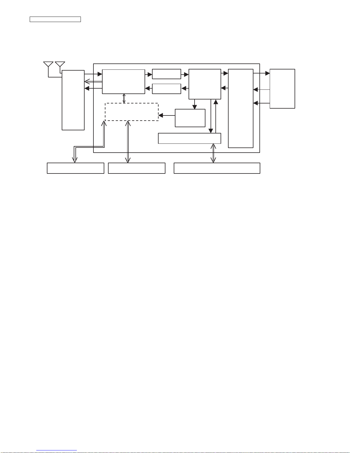
4.2. Block Diagram (Base Unit)
Analog
Front
End
To TEL_LINE
Bridge
Rect D101
Hook Switch
Q141, Q142, Q161
Audio
Bell/Caller ID
Interface
CPU
MICn
LSRp
RINGn
CIDINp
CIDINn
CIDOUT
RINGOUT
BELL
HOOK
CHARGE_DET
Off-Hook Line Voltage
PARADET
A/D
D/A
ADPCM
Codec Filter
DSP
Speech Encoding
Speech Decoding
BMC
Burst Encoding
Burst Decoding
RF
PLL
XTAL2
XTAL1
EEPROM
SCL
SDA
To HANDSET
Limit
Resistor
R371, R372,
D362
Charge
Detector
CHARGE(+)
CHARGE(-)
for KX-PRW120 only
IC302 3.3V IC302 3.3V
REGULATORREGULATOR
Q502Q502
Q501Q501
2.4V
Reg.
1.8V
Reg.
3.3 V
2.4 V
1.8 V
BBIC
IC502
IC501
KX-PRW120 BLOCK DIAGRAM (BASE UNIT)
MOD/DEMOD
DCDC
Converter
Reset
XTAL
X1
X1
MHz
RX
n
RX
p
TX
p
TX
n
DA802
ANT1
ANT2
ANT1
ANT2
ANT1
ANT2
L1
L2
DCP
DCM
FLASH MEMORY
IC601
QSPI
FLASH MEMORY
IC503
RSTN
Pin B8
TAM-CSn
SPI-DI
SPI-DO
SPICLK
QSPI-CS
QSPI-SCK
QSPI-IO 0-3
Q701, Q702
QSPI
Control
SPI
Control
Interrupt
Control
PCM
Control
Wi-Fi module
IC800
SPI_EN
SPI_DO
SPI_DI
SPI_CLK
BB_TX
BB_RX
BB_TX_RES
BB_RX_RES
PCM_FSC
PCM_DO
PCM_DI
PCM_CLK
PORST_N
20.736
3.3 V
L501

11
KX-PRW120W/KX-PRWA10W
4.3. Circuit Operation (Base Unit)
4.3.1. Outline
Base Unit consists of the following ICs as shown in Block Diagram (Bas e Unit) (P.10).
• DECT BBIC (Base Band IC): IC501
- Handling all the audio, signal and data processing needed in a DECT base unit
- Controlling the DECT specific physical layer and radio section (Burst Module Controller section)
- ADPCM code filter for speech encoding and speech decoding (DSP section)
- Echo-cancellation and Echo-suppression (DSP section)
- Any tones (tone, sidetone, ringing tone, etc.) generation (DSP section)
- DTMF receiver (DSP section)
- Clock Generation for RF Module
- ADC, DAC, timer, and power control circuitry
- PLL Oscillator
- Detector
- Compress/Expander
- First Mixer
- All interfaces (ex: QSPI FLASH MEMORY, EEPROM, LED, Analog Front End, etc.)
- Integrated 1.9GHz PA for DECT
• EEPROM: IC502
- Temporary operating parameters (for RF, etc.)
• FLASH MEMORY: IC601
- Voice Prompt (TAM) D/L Area
- ICM/OGM Recording Area
• Additionally,
- Power Supply Circuit (+2.4 V, +1.8 V output)
- Crystal Circuit (20.736 MHz)
- Charge Circuit
- Telephone Line Interface Circuit
• QSPI FLASH MEMORY IC503
- Main Program D/L Area
• Wi-Fi module : IC800
- Handling the audio, signal and data processing related to Wi-Fi.
- Support IEEE802.11b/11g/11n.
- Controlling the connection with the smartphone ap plication.
- Power Supply Circuit (+1.5V output).
12
KX-PRW120W/KX-PRWA10W
4.4. Circuit Operation (Base Unit)
General Description:
(BBIC, Flash Memory, EERROM) is a digital speech/signal processi ng system that implements all the functions of speechcompression, record and playback, and memory management required in a digital telephone answering machine.The BBIC system
is fully controlled by a host processor. The host processor provides activation and control of all that functionsas follows.
4.4.1. BBIC (Base Band IC: IC501)
• Voice Message Recording/Play back
The BBIC system uses a proprietary speech compression technique to record and store voice message in Flash Memory.An
error correction algorithm is used to enable playback of these messages from the Flash Memory.
• DTMF Generator
When the DTMF data from the handset is received, the DTMF signal is output.
• Synthesized Voice (Pre-recorded message)
The BBIC implements synthesized Voice, utilizing the built in speech detector and a Flash Memory, which stored the vocabulary.
• Caller ID demodulation
The BBIC implements monitor and demodulate the FSK/DTMF signals that provide CID information from the Central Office.
• Digital Switching
The voice signal from telephone line is transmitted to the handset or the voice signal from the han dset is transmitted to theTelephone line, etc. They are determined by the signal path route operation of voice signal.
• Block Interface Circuit
RF part, Key scan, Telephone line.
4.4.2. Flash Memory (IC601)
Following information data is stored.
• Voi ce signal
ex: Pre-recorded Greeting message, Incoming message
4.4.3. EEPROM (IC502)
Following information data is stored.
• Settings
ex: message numbers, ID code, Flash Time, Tone/Pulse
RF part
ADPCM
Analog
Front
End
&
Multiplexer
TEL
Line
Interface
Digital
Speech
Processor
Caller ID
Modem
Digital TAM System
Flash Memory IC601
Host CPU
BBIC (IC501)
DECT RF system
TDMA/TDD
Mod/Demod
PA/LNA
ADPCM
Keys/ ChargeEEPROM IC502
13
KX-PRW120W/KX-PRWA10W
4.4.4. Power Supply Circuit
The power is supplied to the DECT BBIC, QSPI FLASH MEMORY, FLASH MEMORY, EEPROM and Charge Contact from AC
Adaptor (+5.5 V) as shown in Fig.101. The power supply is as follows;
• DECT BBIC (IC501):
DC Jack (+5.5 V) → IC302 → IC501
DC Jack (+5.5 V) → IC302 → Q302 → IC501
DC Jack (+5.5 V) → IC302 → D501 → Q501 → IC501
• EEPROM (IC502):
DC Jack (+5.5 V) → IC302 → IC501→ IC502
• FLASH MEMORY (IC601):
DC Jack (+5.5 V) → IC302→ IC501→ IC601
• Charge Contact (CHARGE+):
DC Jack (+5.5 V) → R371 → R372 → D362→ CHARGE+
• QSPI FLASH MEMORY (IC503):
DC Jack (+5.5 V) → IC302 → IC501 → IC503
<Fig.101>
AC Adaptor
* for KX-PRW120 only
DCP
IC302
Q302
IC501
IC503
IC601*
IC502
+5.5 V
1.8 V
Q301
2.4 V
CHARGE+
D362
R372
R371
DC
Jack
3.3 V
DCM
1
2
3
On
DC S
1.8 V
Reset
(IC501(RSTN))
Off

14
KX-PRW120W/KX-PRWA10W
4.4.5. Telephone Line Interface
<Function>
• Bell signal detection
• Clip signal detection
• ON/OFF hook circuit
Bell & Clip (: Calling Line Identification Presentation: Caller ID) signal detection:
In the standby mode, Q141 is open to cut the DC loop current and decrease the ring load.
When ring voltage appears at the L1T (A) and L1R (B) leads (when the telephone rings), the AC ring voltage is transferred as
follows;
•B → P101 → C106 → R106 → R107 → IC501 (CID INp)
•A → C105 → R105 → R108 → IC501 (CID INn)
ON/OFF hook circuit:
In the standby mode, Q104 is open, and connected as to cut the DC loop current and to cut the voice signal. The unit is
consequently in an on-hook condition.
When IC501 detects a ring signal or press the TALK Key onto the handset, Q142 turns on and then Q141 turns on, thus
providing an off-hook condition (DC current flows through the circuit) and the following signal fl ow makes the loop current.
•B → P101 →D101 → Q141 → Q161 → R163 → D101 → A
4.4.6. Transmitter/Receiver
• Audio Circuits and DTMF tone signal circuits.
Base Unit and Handset mainly consist of RF Module and DECT BBIC.
Base Unit and Handset transmit/receive voice signal and data signal through the antenna on carrier frequency.
Signal Path:
*Refer to Signal Route (P.20).
4.4.6.1. Transmitter Block
The voice signal input from the TEL LINE interface goes to DECT BBIC (IC501) as shown in Block Diagram (Base Unit) (P.10)
The voice signal passes through the analog part of IC501 where it is ampli fied and converted to a digi tal audio stream signal.
The burst switch controller processes this stream performing encryption and scrambl ing, adding the various other fields to
produce the GAP (Generic Access Profile) standard DECT frame, assigning to a time slot and channel etc.
In IC501, the carrier frequency is changing, and frequency modulated RF signal is generated.In IC501 ,RF signal is amplified,
and radiated from antenna. Handset detects the voice signal or da ta signal in the circuit same as the following explanation of
Receiver Block.
4.4.6.2. Receiver Block
The signal of 1900 MHz band (1921.536MHz ~ 1928.448MHz) which is input from antenna is input to IC501 as shown in Block
Diagram (Base Unit) (P.10).
In IC501, the signal of 1900 MHz band is downconverted to 864 kHz signal and demodulated, as GAP (Generic Access Profile)
standard DECT frames. It passes through the decoding section burst switch controller where it separates out the frame
information and performs de-encryption and de-scrambling as required. It the n goes to the DSP section where it i s turned back
into analog audio. This is amplified by the analog front end, and goes to the TEL LINE Interface.
4.4.7. WiFi Module
BBIC and WiFi module are connected with 3group signals as shown in Block Diagram (Base Unit) (P.10).
SPI (Serial Peripheral Interface) Control --- Control the data (except Audio data) between BBIC and Wi-Fi module
Interrupt Control --- Control the timing of sending/receiving of BBIC and Wi-Fi module
PCM (Pulse Code Modulation) Control --- Control the Audiol data between BBIC and Wi-Fi module.
When turning ON, it start to communicate between BBIC and WiFi module by SPI Control with Interrupt control to set various
data into the register of WiFi module and then it becomes Stand-by status.
WiFi network data, such as MAC address is transferred to Memory of WiFi module from BBIC's one.
For talk with Smartphone via WiFi, audio signal is modified to PCM signal then communicated.
4.4.8. Parallel Connection Detect Circuit/Auto Disconnect Circuit
Function:
In order to disable call waiting and stutter tone functions when u si ng te leph one s connecte d i n paralle l, it is necessary to have a
circuit that judges whether a telephone connected in parallel is in use or not. T his circuit determines whether the telephone
connected in parallel is on hook or off hook by detecting changes in the T/R voltage.
Circuit Operation:
Parallel connection detection when on hook:
When on hook, the voltage is monitored at pin (N1), (N2) of IC501. There is no parallel connection if the voltage is
0.54 V or higher, while a parallel connection is deemed to exist if the voltage is lower.

15
KX-PRW120W/KX-PRWA10W
Parallel connection detection when off hook:
When off hook, the voltage is monitored at pin (F2) of IC501; the presence/absence of a parallel connection is determined by
detecting the voltage changes.
If the Auto disconnect function is ON and statuses are Hold, receiving ICM, OGM transmitting, BBIC disconnects the line after
detecting parallel connection is off hook.
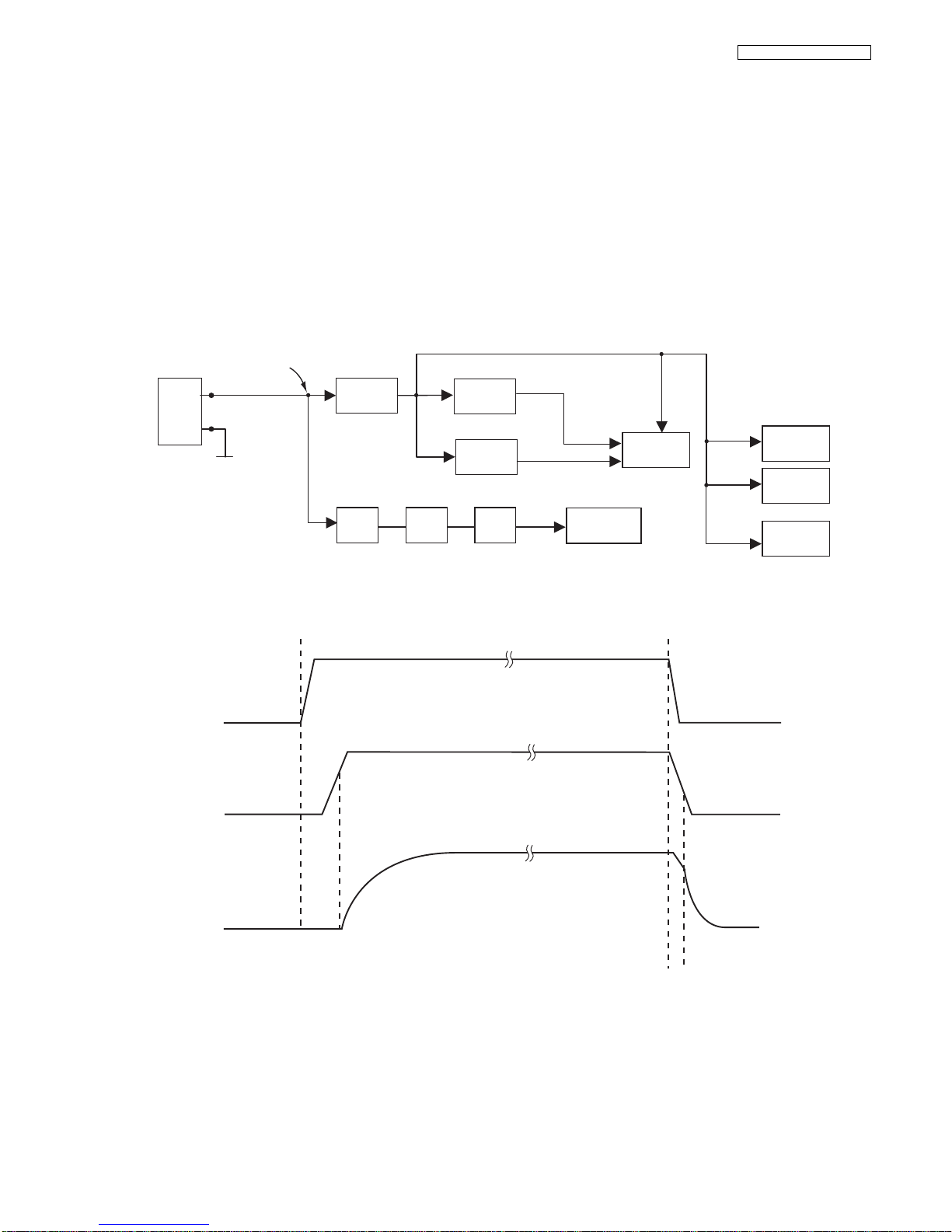
4.4.9. Calling Line Identification (Caller ID)/Call Waiting Caller ID
Function:
Caller ID
The caller ID is a chargeable ID which the user of a telephone circuit obtains by entering a contract with the telephone company
to utilize a caller ID service. For this reason, the operation of this circuit assumes that a caller ID service contract has been
entered for the circuit being used. The data for the caller ID from the telephone exchange is sent during the interval between the
first and second rings of the bell signal. The data from the telephone exchange is a modem signal which is modulated in an FSK
(Frequency Shift Keying) * format. Data
"1" is a 1200 Hz sine wave, and data "0" is a 2200 Hz sine wave. There are two types of
the message format which can be received: i.e. the single messa ge format and plural message format. The plural message
format allows to transmit the name and data code information in addition to the time and telephone number data.
*: Also the telephone exchange service provides other formats.
1st Ring
2 sec
Silent interval 4 sec
2nd Ring
2 sec
0.5 s 575 ms
min 0.5 s
DATA
0.1 Vrms
STD Ring / 20 Hz
Tip-Ring
DATA in
A
B
DATA out
1200 Hz
=DATA "1"
1 bit=833 µs
2200 Hz
=DATA "0 "
70 Vrms
month dayhour minute number
201348700035161504
Single message format
Plural message format
1st Ring
2 sec
718 ms
2nd Ring
0.5 s
DATA
month
day
hour
minute
number
20134870003516
16
DATA CODE NAME
201 John Smith
04

16
KX-PRW120W/KX-PRWA10W
Call Waiting Caller ID
Calling Identity Delivery on Call Waiting (CIDCW) is a CLASS service that allows a customer, while off-hook on an existing call,
to receive information about a calling party on a waited call. The transmission of the calling information takes place almost
immediately after the customer is alerted to the new call so he/she can use this info rmation to decide whether to take the new
call.
Function:
The telephone exchange transmits or receives CAS and ACK signals through each voice RX/TX route. Then FSK d ata and
MARK data pass the following route.
Telephone Line → P101 → C103, R101, C105, R103, C107, R10 5, C104, R102 , C106, R104, C108, R106 → IC501 (H2, H1).
If the unit deems that a telephone connected in parallel is in use, ACK is not returned even if CAS is received, and the
information for the second and subsequent callers is not displayed on the portable display.
CAS
CAS: CPE Alerting Signal
Dual Tone of 2130 Hz, 2750 Hz
-15 dBm (900 ohm load)
80 5 ms
MARK
DATA
0~500 ms
58~75 ms about 300 ms
(be changed by
Information Volume)
Continuance Signal
of 1200 Hz (Data "1")
"FSK"
ACK: Acknowledged Signal
DTMF
"D"
ACK
0~100 ms
60 5 ms
Telephone Exchange
Cordlessphone
Cordlessphone
Signal Flow
Signal Flow
Telephone Exchange
Call Waiting Format
C107
R105
P101
L1T
L1R
SA101
H2
H1
BBIC
IC501
"FSK"
data
Telephone
Line
R103
R101
C103
C105
C108
R106
R104
R102
C104
C106

17
KX-PRW120W/KX-PRWA10W
4.5. Block Diagram (Handset)
QSPI
FLASH MEMORY
IC2
Reset
Reset
Pin B8
ADPCM
Codec
Filter
DSP
Speech
Decoding
Speech
Encoding
BMC
Burst
Decoding
ANT1
Burst
Encoding
RF
PLL
MOD/DEMOD
C1
D1
A4
A5
RXn
ANT1
RXp
TXp
TXn
G1
F1
XTAL
X1
20.736
MHz
BATTERY
T4
ON SWITCH
KEYPAD
Charge
Pump
ROWS
COLUMNS
U5, T6, V5, T7, N1
F3, G2, G3, H2, T11
V12, U13, V14, T12
BBIC
IC1
QSPI
Control
U12
U14
KX-PRWA10 BLOCK DIAGRAM (Handset)
SPI
Control
SPI
FLASH MEMORY
IC4
C9 SPI_EN
+2.8V
C11 SPI_DI
B13 SPI_DO
A14 SPI_CLK
+3.0V
DC/DC
Control
CONVERTER
CPU
LDO_OI_CTRL
CIRCUIT
CONVERTER
DC/DC
Q8, L3
3.0V
Q7
+3.0V
+2.8V
SPEAKER
RECEIVER
MIC
CHARGE
CIRCUIT
CHARGE
CONTACTS
CHARGE(+)
CHARGE_CTRL
CHARGE
EEPROM
SCL
SDA
BATTERY
TERMINAL
R1
VBAT
BATT-
1.8 V
Q6
1.8 V
LCD
RS
RDn
DAB[0-7]
LCD_RESET
CPU
Analog
Front
End
D/A
A/D
U8, V8
U9, V9
K3
K2
H1
J3
R2
R1
B12
A13
M5
M3
J14
J18, J17, J16, L18, M18,
N18, P18,P17
E13
P3
K16
IC3
C16
LCD-BACK LIGHT
KEY LED
A9
LDO_CTRL
CP3V
+2.8V
DC/DC CONVERTER CIRCUIT Q9, L4
WRn
LCD_CS
B15
+3.0V
+1.8V
+3.4V
+3.4V
Q2, Q3, Q4
R4, R7, R8

18
KX-PRW120W/KX-PRWA10W
4.6. Circuit Operation (Handset)
4.6.1. Outline
Handset consists of the following ICs as shown in Block Diagram (Handset) (P.17).
• DECT BBIC (Base Band IC): IC1
- All data signals (forming/analyzing ACK or CMD signal)
- All interfaces (ex: Key, Detector Circuit, Charge, DC/DC Converter, EEPROM, LCD, RF Power Amp.)
- PLL Oscillator
- Detector
- Compress/Expander
- Reception
- Integrated 1.9 GHz PA for DECT
• QSPI FLASH MEMORY: IC2
- Main Program D/L Area
• EEPROM: IC3
- Temporary operating parameters (for RF, etc.)
• SPI FLASH MEMORY: IC4
- Wall paper, Ringer Tone D/L Area.
4.6.2. Power Supply Circuit/Reset Circuit
Circuit Operation:
When power on the Handset, the voltage is as follows;
BATTERY(2.2 V ~ 2.6 V: BATT+) → P1 → L3 → Q8 → Q6 (1.8 V), Q7 (3.0V)
The Reset signal generates IC1 (B8 pin) and 1.8 V.
4.6.3. Charge Circuit
Circuit Operation:
When charging the handset on the Base Unit, the charge current is as follows;
DC+(5.5 V) → R371 → R372 → D362 → CHARGE+(Base) → CHARGE+(Handset) → → Q2 → P1 → BATTERY+...
Battery...
BATTERY- → R1→ GND → CHARGE-(Handset)→ CHARGE-(Base) → GND → DC-(GND)
In this way, the BBIC on Handset detects the fact that the battery is charged.
The charge current is controlled by switching Q4 of Hand se t.
Refer to Fig.101 in Power Supply Circuit (P.13).
4.6.4. Battery Low/Power Down Detector
Circuit Operation:
“Battery Low” and “Power Down” are detected by BBIC which check the voltage from battery.
The detected voltage is as follows;
• Battery Low
Battery voltage: V(Batt) 2.25 V ± 50 mV
The BBIC detects this level and " " starts flashing.
• Power Down
Battery voltage: V(Batt) 2.0 V ± 50 mV
The BBIC detects this level and power down.
1.8 V
Reset
(IC1_B8pin)
Battery +
Q3
R4

19
KX-PRW120W/KX-PRWA10W
4.6.5. Speakerphone
The hands-free loudspeaker at SP+ and SP- is used to generate the ring alarm.

20
KX-PRW120W/KX-PRWA10W
4.7. Signal Route
SIGNAL ROUTE
ROUTE
IN
OUT
SIGNAL
DTMF TONE
TEL OUT
(to Tel Line)
CDL TX
(to Tel Line)
CDL RX
(from Tel Line)
DTMF TONE
TEL IN
(from Tel Line)
SP-PHONE TX
(to Tel Line)
SP-PHONE RX
(from Tel Line)
Caller ID
(from Tel Line)
(BASE UNIT)
B - P101 - C106 - R106 - R107 - IC501 (CIDINp) IC501 (TXp) C819
A - C105 - R105 - R108 - IC501 (CIDINn) IC501 (TXn)
(BASE UNIT)
IC501 (LSRp) - C184 - Q161 - Q141 - D101 A
(BASE UNIT)
A D101 - Q141 - Q161 - R164 - C173 - R178 - IC501 (MICn)
P101
- B
(BASE UNIT)
from HANDSET
ANT1 - C894 DA802 IC501 (RXn)
ANT2 - C893 IC501 (RXp)
IC501 (LSRp) - C184 - Q161 - Q141 - D101 A
P101- B
B - P101
- C819 - DA802 C894 - ANT1
to HANDSET
(HANDSET)
from BASE UNIT ANT - C50
(BASE UNIT)
A
D101 - Q141 - Q161 - R164 - C173 - R178 - IC501 (MICn) IC501 (TXp)
B - P101 IC501 (TXn)
C893 - ANT2
IC1 (D1)
IC1 (C1)
IC1 (K3) - RECEIVER (+)
IC1 (K2) - RECEIVER (–)
DA802 –– C894 - ANT1
– C893 - ANT2
to HANDSET
to HANDSET
(HANDSET)
from BASE UNIT ANT - C50
–– IC1 (D1) ––– IC1 (U8, V8) - SP (–)
– IC1 (C1) – – IC1 (U9, V9) - SP (+)
(BASE UNIT)
A D101 - Q141 - Q161 - R164 - C173 - R178 - IC501 (MICn)
B - P101
–– IC501 (TXp) - C819 - DA802 –– C894 - ANT1
– IC501 (TXn) C893 - ANT2
(HANDSET)
MIC (+) -
C10 - R17 - IC1 (J3) IC1(A4)
MIC (–) -
C9 - R16 -
IC1 (H1)
IC1(A5) C51 - C50 - ANT to BASE
(BASE UNIT)
from HANDSET
ANT1 - C894 DA802 IC501 (RXn)
ANT2 - C893 IC501 (RXp)
IC501 (LSRp) - C184 - Q161 - Q141 - D101 A
P101- B
(HANDSET)
MIC (+) -
C10 - R17 - IC1 (J3) IC1(A4)
MIC (–) -
C9 - R16 - IC1 (H1) IC1(A5) C51 - C50 - ANT to BASE

21
KX-PRW120W/KX-PRWA10W
SIGNAL ROUTE
ROUTE
IN
OUT
SIGNAL
Memo/OGM
Recording
(from Handset)
ICM Recording
(from Tel Line)
(BASE UNIT)
from HANDSET
ANT1 - C894 –– DA802
IC501 (RXn) ––
ANT2 - C893 – IC501 (RXp) –
IC501 (LSRp) - IC601 (5)
(BASE UNIT)
A
–––––––– D101 - Q141 - Q161 - R164 - C173 - R178 - IC501 (MICn) - IC501 (SPI_DO) - IC601 (5)
B - P101
–
Message Play
(to Handset)
(BASE UNIT)
IC601 (2) - IC501 (SPI_DI) IC501 (TXp) C819 -
(BASE UNIT)
IC601 (2) - IC501 (SPI_DI) - IC501 (LSRp) - C184 - Q161 - Q141 - D101 A
Message Play
(to Tel Line)
IC501 (TXn)
DA8 02
C894- ANT1
C893 - ANT2
to HANDSET
(HANDSET)
from BASE UNIT ANT - C50 –– IC1 (D1)
– IC2 (C1)
IC1 (U8, V8) - SP (–
)
IC1 (U9, V9) - SP (+)
P101 - B
for KX-PRW120 only
(HANDSET)
MIC (+) -
C10 - R17 - IC1 (J3) IC1(A4)
MIC (–) -
C9 - R16 - IC1 (H1) IC1(A5) C51
- C50 - ANT to BASE
Wi-Fi TX
(to Tel Line)
(BASE UNIT)
fromSmartPhone
WIFITX - C865 - IC800 (WIFITX)
WIFIRX - C866 - IC800 (WIFIRX)
IC800 (PCMDTX) - IC501 (PCM_DI)
IC501 (LSRp) - C184 - Q161 - Q141 - D101
A
P101-B
Wi-Fi RX
(to Tel Line)
(BASE UNIT)
A
–––––––– D101 - Q141 - Q161 - R164 - C173 - R178 - IC501 (MICn)
B - P101
–
IC501 (PCM_DO) - IC800 (PCMDRX) - IC800 (WIFITX) - C865 - WIFITX
toSmartPhone

22
KX-PRW120W/KX-PRWA10W
5 Location of Controls and Components
Refer to the Operating Instructions.
Note:
You can download and refer to the Operating In structions (Instruction book) on TSN Server.
6 Installation Instructions
Refer to the Operating Instructions.
Note:
You can download and refer to the Operating In structions (Instruction book) on TSN Server.
7 Operating Instructions
Refer to the Operating Instructions.
Note:
You can download and refer to the Operating In structions (Instruction book) on TSN Server.
7.1. For Service Hint
Items Contents
Battery
You could use other rechargeable batteries sold in a market, but the unit is not guaranteed to work
properly.
The battery strength may not be indicated correctly if the battery is disconnected and connected again,
even after it is fully charged. In that case, by recharging the battery as mentioned in the Operating
Instructions, you will get a correct indication of the battery strength.
Recall Earth Recall feature is not supported in this model.

23
KX-PRW120W/KX-PRWA10W
8 Service Mode
8.1. Engineering Mode
8.1.1. Base Unit
Important:
Make sure the address on LCD is correct when entering new data. Otherwise, you may ruin the unit.
9).
Press (off) to return to standby mode.
After that, turn the base unit power off and then power on.
Menu
1). Press {}
2). Select "Initial Setup" using , , , or
then press
{OK} .
H/S key operation
H/S LCD
{^}
4). Enter "7", "2", "6", "2", "7", "6", "6", "4".
Note: 7262 7664 = PANA SONI
(see letters printed on dial keys)
6). Enter "
", " ", " ", " " (Address). (*1)
7). Enter "
", " " (New Data). (*1)
5). Select "Write EEP" using or
then press
{OK}
.
{^} {V}
3). Select "Line Setup" using or
then press
{OK}
{^} {V}
8)
. Press , a long confirmation beep
will be heard.
{OK}
{V}
{>}
{>}
.
.
Initial Setup
OK
Intercom
C
C
OK
Back
Initial Setup
Time Settings
Handset Name
Key Finder Setup
Caller Barred
d
d
Ringer Setup
OK
Back
Initial Setup
Auto Talk
Privacy Mode
d
d
Area Code
Caller List
C
C
OK
Intercom
Call Restrict
OK
Back
Service Mode
Gets S/W Ver.
d
d
Read EEP
Write EEP
OK
C
Set Addr.:
OK
Set Addr.:
Back
Default Data
OK
C
Set Addr.:
New Data
Soft keys
Navigator key/
?
(Volume) key
Dial keypad
{R/ECO}
R: Recall/Flash
ECO: Eco mode shortcut key
{ic} (Off/Power)
Line Setup

24
KX-PRW120W/KX-PRWA10W
Frequently Used Items (Base Unit)
ex.)
Note:
(*1) Refer to Registering a Handset to a Base Unit in the Operating Instructions.
(*2) When you enter the address or New Data, please refer to the table below.
Items Address Default Data New Data Remarks
C-ID(FSK) sensitivity 07 5D/07 5C 00/51 00/39
(3 dB up)
00/28
(6 dB up)
When the hex change from 00/51 to 00/39 or
00/28, gain increase by 3 dB or 6 dB.
Frequency 00 08/00 07 04/4A - - Use these items in a READ-ONLY mode to
confirm the contents. Careless rewriting may
cause serious damage to the computer system.
ID 00 02~00 06 Given value - -
Bell length 03 F9 3C (6 sec) (*3) 1E (3 sec) 14 (2 sec) This is time until bell stops ringing.
(Unit: 100 msec)
Desired Number (hex) Input Keys Desired Number (hex) Input Keys
00 A[R] + 0
11 B[R] + 1
.. C[R] + 2
.. D[R] + 3
.. E[R] + 4
99 F[R] + 5

25
KX-PRW120W/KX-PRWA10W
8.1.2. Handset
Important:
Make sure the address on LCD is correct when entering new data. Otherwise, you may ruin the unit.
8).
Press (off) to return to standby mode.
After that, remove and reinsert the batteries.
Press the Power button for
about 1 second if
the power is not turned on.
H/S key operation
H/S LCD
3). Enter "7", "2", "6", "2", "7", "6", "6", "4".
Note: 7262 7664 = PANA SONI
(see letters printed on dial keys)
5). Enter "
", " ", " ", " " (Address). (*1)
6). Enter "
", " " (New Data). (*1)
7)
. Press , a long confirmation beep
will be heard.
{OK}
Initial Setup
OK
Intercom
C
C
Base Unit PIN
Caller List
C
C
OK
Intercom
OK
Back
Service Mode
Gets S/W Ver.
d
d
Read EEP
Write EEP
OK
C
Set Addr.:
OK
Set Addr.:
Back
Default Data
OK
C
Set Addr.:
New Data
Menu
1). Press {}
4). Select "Write EEP" using or
then press
{OK}
.
{^} {V}
2). Select "Initial Setup" using , , , or
then press
{OK} .
{^}
{V}
{>}
{>}
.
Soft keys
Navigator key/
?
(Volume) key
Dial keypad
{R/ECO}
R: Recall/Flash
ECO: Eco mode shortcut key
{ic} (Off/Power)

26
KX-PRW120W/KX-PRWA10W
Frequently Used Items (Handset)
ex.)
Note:
(*1) When you enter the address or New Data, please refer to the table below.
(*2) Use these items in a READ-ONLY mode to confirm the contents. Careless rewriting may cause seri ous damage to the
handset.
Items Address Default Data New Data Possible Adjusted
Value MAX (hex)
Possible Adjusted
Value MIN (hex)
Remarks
Sending level 05 07 Adjusted value Given value FF D0 (*2)
Receiving level 05 08 Adjusted value Given value FF D0 (*3)
Battery Low 00 09 70 - - -
(*4)
Frequency 00 08/00 07 04/4A - - -
ID 00 02~00 06 Given value - - -
Desired Number (hex.) Input Keys Desired Number (hex.) Input Keys
00 A[R] + 0
11 B[R] + 1
.. C[R] + 2
.. D[R] + 3
.. E[R] + 4
99 F[R] + 5

27
KX-PRW120W/KX-PRWA10W
8.2. EEPROM LAYOUT (Handset)
8.2.1. Scope
The purpose of this section is to describe the layout of the EEPROM (IC3) for the KX-PRWA10 Handset.
The EEPROM contains hardware, software, and user specific parameters. Some parameters are set during production of the
handset, some are set by the user when configuring the handset, and some during normal use of the phone.
8.2.2. Introduction
The handset uses a 64k bit serial EEPROM (IC3) for storing volatile parameters. All parameters are set up before the handset
the factory. Some of these are vital for the operation of the hardware so a set of default parameters is programmed before the
actual hardware fine-tuning can be initiated. This document lists all default settings with a short description.
This document lists all default parameters with a short description.
8.2.3. EEPROM contents
MMI Setting:
MMI1 Setting:
Initial Type Description
F The data initialized by only F command
0 The data initialized by F and 0 command
1 The data initialized by F, 0 and 1 command
2 The data initialized by F, 0, 1 and 2 command
3 The data initialized by all command (F, 0, 1, 2, 3)
Country Setting Description
x Default - no specific country setting, so revert to default value.
Address Initial
Type
Name Description Default value Country
Setting
04 1B 3 EEP_Language Selected Language for LCD
GERMAN:0 ENGLISH:1 SPANISH:2 NORWEGIAN:3
FRENCH:4
ITALIAN:5 DENISH:6 DUTCH:7 SWEDISH:8
FINNISH:9
GREEK:10 TURKISH:11 HUNGARIAN:12
PORTUGUESE:13 RUSSIAN:14
POLISH:15 SLOVAKIAN:16 CZECH:17 CROATIAN:18
CATALAN:19
UKRINIAN:20 SPANISHMEX:21 SLOVENIAN:22
ESTNIAN:23 LITHUANIAN:24
LATVIAN:25 ROMANIAN:26 BULGARIAN:27
MACEDONIAN:29
ALBANIAN:30 PORTUGUESEMEX:31
ENGLISH(USA):32 HEBREW:33
ARABIC:34 PERSIA:35 HANTAI:36 HANTAI(HK):37
RUSSIAN(BX):38
BELARUS:39 KAZAKHSTAN:40 UZBEKISTAN:41
TAJIKISTAN:42
TURKMENISTAN:43 AZERBAIJAN:44 ARMENIA:45
MOLDOV:46
CANADAENGLISH:48 USSPANISH:49 USFRENCH:50
PORTUGUESE:51 ENGLISH(AZ):52
0x01 x
Address Initial
Type
Name Description Default value Country
Setting
00 63 F EEP_LcdContrastOffset Set the VCOM offset voltage 0xAC x
 Loading...