

Page 1
ST
IC DRIVABLE PC BOARD
RELAY FOR INDUCTIVE
LOAD SWITCHING
VDE
ST RELAYS
RoHS Directive compatibility information
http://www.mew.co.jp/ac/e/environment/
FEATURES
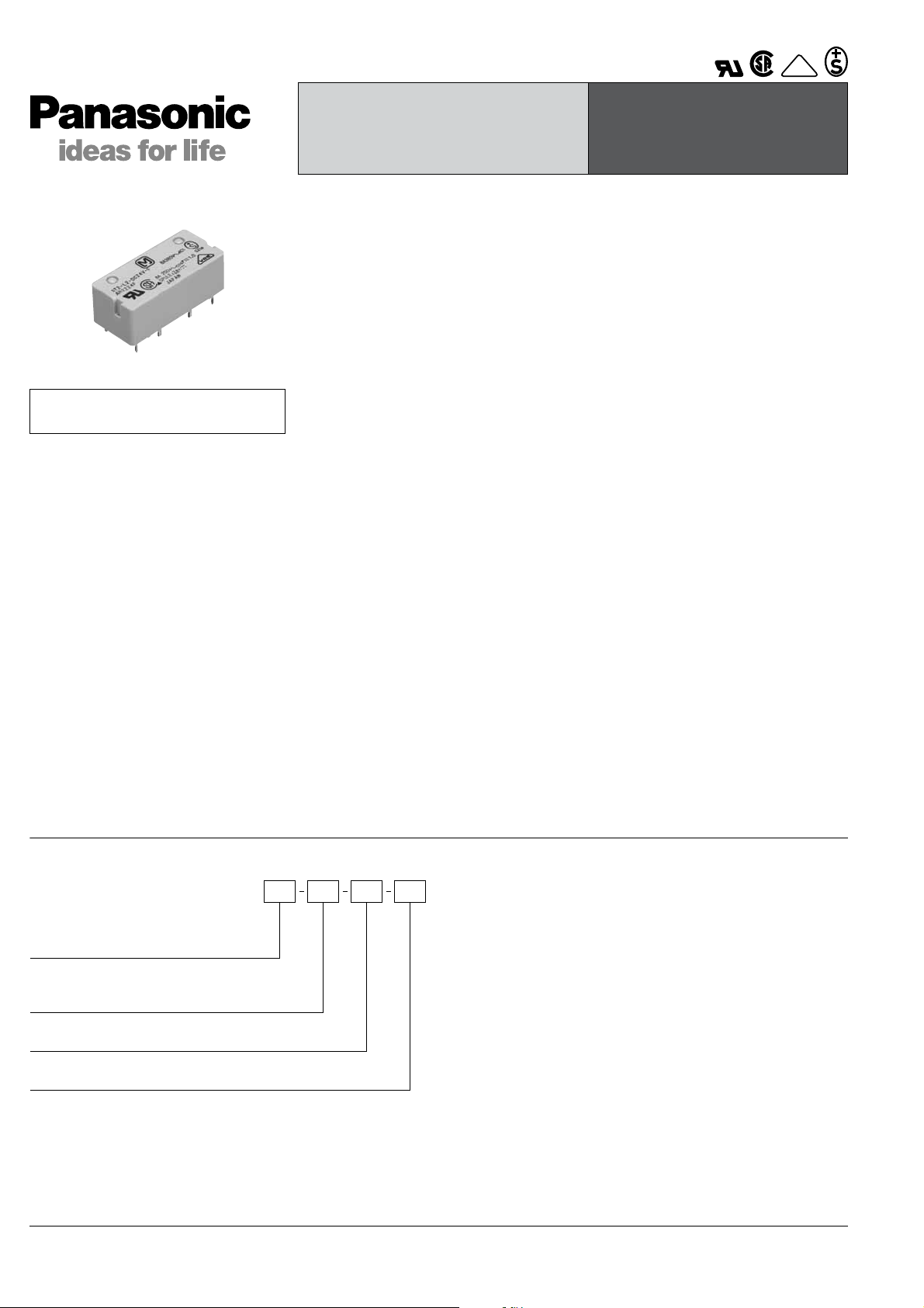
1. Even with small form factor,
sensitive enough for direct IC-driving
The dimensions of this high-density 4gap balanced armature are 31 mm × 14
mm × 11 mm 1.220 inch × .551 inch ×
.433 inch. Despite this small size, high
sensitivity is achieved by a mechanism
that incorporates high-efficiency
polarized magnetic circuits along with our
exclusive spring alignment method. With
an minimum operating power of about
150 mW, nominal operating power of 240
mW, this relay can be directly driven by
transistor or chip controllers.
2. High switching capability
High contact pressure, low contact
bounce, and forced separation structure
that radically improves resistance to
contact welding (1 Form A 1 Form B type
equivalent to TV-3). Strong against lamp
inductive loads, maximum switching
capacity has reached 3,040 VA (8A 380V
AC).
3. High breakdown voltage – Optimal
for control in 250 V power circuits
High breakdown voltage has been
achieved. Between contacts and coil of
3,750 Vrms; Surge breakdown voltage
between coil and contact of 6,000 V, and
between open contacts of 1,200 Vrms
mean that these relays are suitable even
for 250 V power circuit control.
4. Improved stability
Conforms to all types of safety
standards.
Insulating distance of more than 3 mm
secured. Complies with Japan Electrical
Appliance and Material Safety Law
requirements for operating 200 V power
supply circuits, and conforms with UL,
CSA and VDE standards.
5. Latching types available
In addition to single side stable types,
convenient 2 coil latching types with
memory functions are also available.
Moreover, we offer 2 Form A
specifications which, with double pole
switching for applications such as 250 V
power circuit switching, can enable safer
designs.
6. Automatic cleaning possible
The sealed design means that these
relays can undergo immersion in
automatic washing systems and are
suitable for automatic soldering. Even in
difficult environments, the contacts
remain reliable.
7. Easy to design PC board patterns
Features 4/10 dual-in-line terminals.
Because the lead spacing has a pitch
greater than 7.54 mm .297 inch,
designers can make easy adjustments
with the width of the land size. This, along
with the large insulation distance,
simplifies the drawing of PC board
patterns.
8. To improve soldering efficiency,
preapplication of solder to the
terminals is recommended.
About Cd-free contacts
We have introduced Cadmium free type
products to reduce Environmental
Hazardous Substances.
(The suffix “F” should be added to the
part number)
Please replace parts containing
Cadmium with Cadmium-free products
and evaluate them with your actual
application before use because the life of
a relay depends on the contact material
and load.
ORDERING INFORMATION
ST F
Contact arrangement
1: 1 Form A 1 Form B
2: 2 Form A
Operating function
Nil:
Single side stable
L2:
2 coil latching
Coil voltage
DC 3, 5, 6, 9, 12, 24, 48 V
Contact material
F: AgSnO2 type contact
Note: UL/CSA, VDE, SEV type is standard.
All Rights Reserved © COPYRIGHT Matsushita Electric Works, Ltd.
Page 2
TYPES
Contact arrangement Nominal coil voltage
3V DC ST1-DC3V-F ST1-L2-DC3V-F
5V DC ST1-DC5V-F ST1-L2-DC5V-F
6V DC ST1-DC6V-F ST1-L2-DC6V-F
1 Form A 1 Form B
2 Form A
Standard packing: Tube: 50 pcs.; Case: 500 pcs.
9V DC ST1-DC9V-F ST1-L2-DC9V-F
12V DC ST1-DC12V-F ST1-L2-DC12V-F
24V DC ST1-DC24V-F ST1-L2-DC24V-F
48V DC ST1-DC48V-F ST1-L2-DC48V-F
3V DC ST2-DC3V-F ST2-L2-DC3V-F
5V DC ST2-DC5V-F ST2-L2-DC5V-F
6V DC ST2-DC6V-F ST2-L2-DC6V-F
9V DC ST2-DC9V-F ST2-L2-DC9V-F
12V DC ST2-DC12V-F ST2-L2-DC12V-F
24V DC ST2-DC24V-F ST2-L2-DC24V-F
48V DC ST2-DC48V-F ST2-L2-DC48V-F
Single side stable 2 coil latching
Part No. Part No.
RATING
1. Coil data
1) Single side stable
Nominal coil
voltage
3V DC
5V DC 47mA 105Ω
6V DC 40mA 150Ω
9V DC 25mA 360Ω
12V DC 20mA 600Ω
24V DC 10mA 2,400Ω
48V DC 4.7mA 9,000Ω
Pick-up voltage
(at 20°C 68°F)
80%V or less of
nominal voltage
(Initial)
Drop-out voltage
(at 20°C 68°F)
10%V or more of
nominal voltage
(Initial)
2) 2 coil latching
Nominal coil
voltage
3V DC
5V DC 45mA 45mA 110Ω 110Ω
6V DC 37.5mA 37.5mA 155Ω 155Ω
9V DC 25mA 25mA 360Ω 360Ω
12V DC 18.8mA 18.8mA 640Ω 640Ω
24V DC 10mA 10mA 2,400Ω 2,400Ω
48V DC 4.7mA 4.7mA 10,200Ω 10,200Ω
Set voltage
(at 20°C 68°F)
80%V or less of
nominal voltage
(Initial)
Reset voltage
(at 20°C 68°F)
80%V or less of
nominal voltage
(Initial)
Nominal operating
current
[±10%] (at 20°C 68°F)
75mA 38Ω
Nominal operating
current
[±10%] (at 20°C 68°F)
Set coil Reset coil Set coil Reset coil Set coil Reset coil
75mA 75mA 40Ω 40Ω
Coil resistance
[±10%] (at 20°C 68°F)
Coil resistance
[±10%] (at 20°C 68°F)
Nominal operating
power
240mW
Nominal operating
power
240mW 240mW
ST
Max. allowable voltage
(at 20°C 68°F)
150%V of
nominal voltage
Max. allowable voltage
(at 20°C 68°F)
150%V of
nominal voltage
All Rights Reserved © COPYRIGHT Matsushita Electric Works, Ltd.
Page 3

ST
2. Specifications
Characteristics Item Specifications
Arrangement 1 Form A 1 Form B, 2 Form A
Contact
Rating
Electrical
characteristics
Mechanical
characteristics
Expected life
Conditions
Unit weight Approx. 10g .353 oz
Notes: *1 This value can change due to the switching frequency, environmental conditions, and desired reliability level, therefore it is recommended to check this with the
actual load.
*2 Wave is standard shock voltage of ±1.2×50µs according to JEC-212-1981
*3 Refer to 6. Conditions for operation, transport and storage mentioned in AMBIENT ENVIRONMENT
Contact material Au-flashed AgSnO2 type
Initial contact resistance, max. Max. 30 mΩ (By voltage drop 6 V DC 1A)
Max. switching power (resistive load) 3,040 VA, 150 W
Max. switching voltage 380 V AC, 250 V DC
Max. switching current 8 A
Minimum operating power 150mW (Single side stable, 2 coil latching)
Nominal operating power 240mW (Single side stable, 2 coil latching)
Min. switching capacity (Reference value)*
Insulation resistance (Initial)
(at 25°C, 50% relative humidity)
Breakdown voltage
(Initial)
Between open contacts 1,200 Vrms for 1 min. (Detection current: 10 mA)
Between contact sets 2,000 Vrms for 1 min. (Detection current: 10 mA)
Between contact and coil 3,750 Vrms for 1 min. (Detection current: 10 mA)
Surge breakdown voltage (Initial)*
Operate time [Set time] (at 20°C 68°F)
Release time [Reset time] (at 20°C 68°F)
Temperature rise (at 60°C 140°F)
Shock resistance
Vibration resistance
Functional Min. 196 m/s
Destructive Min. 980 m/s2 (Half-wave pulse of sine wave: 6 ms.)
Functional 10 to 55 Hz at double amplitude of 2 mm (Detection time: 10µs.)
Destructive 10 to 55 Hz at double amplitude of 3 mm
1
100 mA 5V DC
Min. 1,000MΩ (at 500V DC)
Measurement at same location as “Initial breakdown voltage” section.
2
6,000 V (Between contact and coil)
Max. 15 ms [Max. 15 ms]
(Nominal voltage applied to the coil, excluding contact bounce time.)
Max. 10 ms [Max. 15 ms]
(Nominal voltage applied to the coil, excluding contact bounce time.) (without diode)
Max. 55°C
(By resistive method, nominal voltage applied to the coil; contact carrying current: 8A.)
2
(Half-wave pulse of sine wave: 11 ms; detection time: 10µs.)
Mechanical Min. 107 (at 180 cpm)
Electrical Min. 105 (8 A 250 V AC resistive) (ON : OFF = 1 s : 5 s)
Ambient temperature: –40°C to +60°C –40°F to +140°F;
Conditions for operation, transport and storage*
3
Humidity: 5 to 85% R.H. (Not freezing and condensing at low temperature)
Max. operating speed 30 cps
REFERENCE DATA
1. Max. switching power 2. Coil temperature rise 3. Influence of adjacent mounting
10
5
2
1
Current, A
0.5
0.2
0.1
AC resistive load
AC
inductive load
(cosϕ =0.4)
DC resistive load
10 20 50 100 200 300
Voltage, V
100
90
80
70
60
Contact current 8A
50
40
Temperature rise, °C
30
20
10
0
0A
0.2 0.4 0.6 0.8 1.0 1.2
Coil operating power, W
Rated of change, %
-10
-20
-30
-40
40
30
20
10
0
Drop-out voltage
Pick-up voltage
5101520
Inter-relay distance, mm
All Rights Reserved © COPYRIGHT Matsushita Electric Works, Ltd.
Page 4

DIMENSIONS (Unit: mm inch)
2 coil latching
types only.
8-DIA. 1.4
.055
2.54
.100
2.54
.100
12–+34
+–
5678
External dimensions
31.0
1.220
11.0
.433
0.3
.012
3.5 .138
7.62
.300
7
85
7.62
10.16
.300
.400
0.3 .012
1.0
.039
1.0 1.0
.039 .039
0.6 dia. .024 dia.
4321
6
General tolerance: ±0.5 ±.020
1 Form A 1 Form B 2 Form A 1 Form A 1 Form B 2 Form A
0.5
.020
Single side stable 2 coil latching
14
–+
14
.551
10.16
.400
Schematic (Bottom view)
14
–+
PC board pattern (Bottom view)
Tolerance: ±0.1 ±.004
12
–+
34
+–
ST
5678
(Deenergized condition) (Reset condition)
NOTES
1. PC board patterns for 2 coil latching
types
When applying relays in power supply
operation circuits for finished products
regulated by the Electrical Appliance and
Material Safety Law, use the pattern
shown below.
1Te rminal No. 2 3 4
2. Soldering should be done under the
following conditions:
1)
250°C 482°F within 10s
300°C 572°F within 5s
350°C 662°F within 3s
2) For automatic cleaning, the boiling
method is recommended. Avoid
ultrasonic cleaning which subjects the
relays to high frequency vibrations, which
may cause the contacts to stick.
It is recommended that a fluorinated
hydrocarbon or other alcoholic solvents
be used.
For Cautions for Use, see Relay Technical Information.
5678
5678
3. When using, please be aware that
the a contact and b contact sides of 1
Form A and 1 Form B types may go on
simultaneously at operate time and
release time.
All Rights Reserved © COPYRIGHT Matsushita Electric Works, Ltd.
Page 5

ST
VDE
ST relay socket
ST-PS
PC board terminal socket
ST-SS
Solder terminal socket
RoHS Directive compatibility information
http://www.mew.co.jp/ac/e/environment/
FEATURES
1. Possible to fit or remove the chassis
with one touch (t = 0.6 mm to 2.2 mm
.024 inch to .087 inch)
2. Easy design of PC board pattern
(2.54 mm x 4 pitch DIL terminal array)
ACCESSORIES
ST RELAYS
SOCKET
3. Complies with Japan Electrical
Appliance and Material Safety Law.
(UL and VDE certification)
SPECIFICATIONS
Item Specifications
Breakdown voltage (Initial)
Insulation resistance (Initial) Min. 1,000 MΩ between terminals (500V DC)
Heat resistance 150°C 302°F for 1 hr
Max. continuous current 10 A
Relay insertion life 15 times
DIMENSIONS
ST-PS ST-SS
1.05
.041
10.16
.400
7.62
.300
8172635
31.6
1.244
35.4
1.394
7.62
.300
4
Between contact and coil: 4,000 Vrms for 1 min. (Detection current: 10 mA)
Between contact and terminal: 2,000 Vrms for 1 min.
(Unit: mm inch)
4
.158
0.3
.012
.169
16.6
.654
4.3
10.16
0.27
.011
.400
14.6
.575
5.5
.217
4. High breakdown voltage.
16.4
.646
10.16
.400
7.62
.300
31.6
1.244
35.4
1.394
8172635
2.3
.090
7.62
.300
4
.158
16.4
5.5
.217
.646
0.3
.012
5.3
.209
10.16
.400
0.27
.011
14.6
.575
16.6
.654
4
PRECAUTIONS FOR USE (SOCKET)
1. PC board mounting method
PC board pattern
Contact
terminal
interval
Coil
terminal
interval
87 65
12 34
8-1.5 DIA.
8-.060 DIA.
2.54
.100
2.54
.100
The terminal configuration is symmetrical
on the left and right, so an arrow mark
is stamped on the socket to prevent misinsertion. We recommend printing the
same arrow mark on the component
mounting side (side opposite from
pattern) of the PC board. In this case, the
terminal configuration becomes the
terminal nos. noted near the drilling
holes.
2. Chassis cutout
Chassis cutting dimensions
A side
If the chassis hole is punched with a
press, set so the release R on the front
side (A side).
The range for chassis thickness is 0.6 to
2.2 mm .024 to .087 inch.
32.5±0.1
1.280±.004
Press
15.0±0.2
.591±.008
Claw for chassis
fastening
Chassis t = 0.6 to 2.2
.024 to .087
3. Relay mounting and removal
(1) Align the directions of the relay and
socket.
Relay
(2) Insert the relay all the way in, so it is
securely in place.
Hinge
mechanism
(3) Press the part indicated by A in the B
direction, and fasten by placing the hook
on the relay.
Relay case
cross-section
A
B
(Fastening complete)(Before fastening)
(4) When removing the relay, completely
release the hooks on both sides and pull
the relay out.
All Rights Reserved © COPYRIGHT Matsushita Electric Works, Ltd.
 Loading...