

ORDER NO.VM1501005CE
High Definition Video Camera
Model No. HC-V270PP
HC-V270PU
HC-V270EB
HC-V270EC
HC-V270EE
HC-V270EF
B27
HC-V270EG
HC-V270EP
HC-V270GC
HC-V270GK
HC-V270GN
HC-V270GW
HC-V260EE
Colour
(K)...........Black Type
(R)...........Red Type (only HC-V270EG/EP/GC/GK)
(W)...........White Type (only HC-V270GC/V260EE)
© Panasonic Corporation 2015 Unauthorized copying and distribution is a violation of law.
TABLE OF CONTENTS
PAG E PAG E
1 Safety Precautions -----------------------------------------------3
1.1. General Guidelines ----------------------------------------3
1.2. Leakage Current Cold Check ---------------------------3
1.3. Leakage Current Hot Check (See Figure. 1) --------3
2Warning--------------------------------------------------------------4
2.1. Prevention of Electrostatic Discharge (ESD)
to Electrostatically Sensitive (ES) Devices ----------4
2.2. How to Recycle the Lithium Ion Battery (U.S.
Only)-----------------------------------------------------------4
2.3. Caution for AC Cord (For EB/GC) ---------------------5
2.4. How to Replace the Lithium Battery -------------------6
3 Service Navigation------------------------------------------------7
3.1. Introduction --------------------------------------------------7
3.2. General Description About Lead Free Solder
(PbF) ----------------------------------------------------------7
3.3. How to Define the Model Suffix (NTSC or PAL
model)---------------------------------------------------------8
3.4. Formatting----------------------------------------------------9
3.5. Baking of replacement IC and defective P.C.B.
----------------------------------------------------------------10
4 Specifications ---------------------------------------------------- 11
5 Location of Controls and Components------------------ 13
6 Service Mode ----------------------------------------------------- 16
6.1. Model/Destination Settings ---------------------------- 17
6.2. Lock Search and Error History Indication ---------- 18
6.3. Power ON Self Check Result Display--------------- 19
6.4. Adjustment function for the Service ----------------- 20
6.5. Restore the backed up adjustment data------------ 21
6.6. Touch Panel Calibration -------------------------------- 22
6.7. NFC Initialization (HC-V270 only)-------------------- 22
7 Service Fixture & Tools --------------------------------------- 23
7.1. Service Fixture and Tools ------------------------------ 23
7.2. When Replacing the Main P.C.B. -------------------- 23
7.3. Service Position ------------------------------------------ 23
8 Disassembly and Assembly Instructions --------------- 24
8.1. Disassembly Flow Chart for the Unit ---------------- 24
8.2. PCB Location---------------------------------------------- 25
8.3. Disassembly Procedure for the Unit ---------------- 26
9 Measurements and Adjustments -------------------------- 43
9.1. Electric Adjustment --------------------------------------43
10 Factory Setting--------------------------------------------------- 55
10.1. How To Turn On The Factory Settings? ------------ 55
10.2. What Is The Factory Settings? ----------------------- 56
11 Block Diagra m --------------------------------------------------- 57
11.1. Overall Block Diagram ----------------------------------57
11.2. Camera/System Control Circuit Block
Diagram----------------------------------------------------- 58
11.3. Video/Audio Signal Process(1) Circuit Block
Diagram----------------------------------------------------- 59
11.4. Video/Audio Signal Process(2) Circuit Block
Diagram----------------------------------------------------- 60
11.5. Lens Drive Circuit Block Diagram -------------------- 61
11.6. Power Supply Circuit Block Diagram---------------- 62
12 Wiring Connection Diagram --------------------------------- 63
12.1. Interconnection Diagram ------------------------------- 63
2
1 Safety Precautions
1.1. General Guidelines
1. IMPORTANT SAFETY NOTICE
There are special components used in this equipment
which are important for safety. These parts are marked by
in the Schematic Diagrams, Circuit Board Layout,
Exploded Views and Replacement Parts List. It is essen-
tial that these critical parts should be replaced with manu-
facturer’s specified parts to prevent X-RADIATION,
shock, fire, or other hazards. Do not modify the original
design without permission of manufacturer.
2. An Isolation Transformer should always be used during
the servicing of AC Adaptor whose chassis is not isolated
from the AC power line. Use a transformer of adequate
power rating as this protects the technician from acci-
dents resulting in personal injury from electrical shocks. It
will also protect AC Adaptor from being damaged by acci-
dental shorting that may occur during servicing.
3. When servicing, observe the original lead dress. If a short
circuit is found, replace all parts which have been over-
heated or damaged by the short circuit.
4. After servicing, see to it that all the protective devices
such as insulation barriers, insulation papers shields are
properly installed.
5. After servicing, make the following leakage current
checks to prevent the customer from being exposed to
shock hazards.
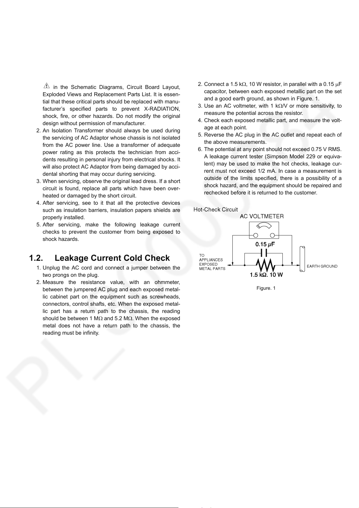
1.3. Leakage Current Hot Check (See Figure. 1)
1. Plug the AC cord directly into the AC outlet. Do not use
an isolation transformer for this check.
2. Connect a 1.5 k, 10 W resistor, in parallel with a 0.15 F
capacitor, between each exposed metallic part on the set
and a good earth ground, as shown in Figure. 1.
3. Use an AC voltmeter, with 1 k/V or more sensitivity, to
measure the potential across the resistor.
4. Check each exposed metallic part, and measure the volt-
age at each point.
5. Reverse the AC plug in the AC outlet and repeat each of
the above measurements.
6. The potential at any point should not exceed 0.75 V RMS.
A leakage current tester (Simpson Model 229 or equiva-
lent) may be used to make the hot checks, leakage cur-
rent must not exceed 1/2 mA. In case a measurement is
outside of the limits specified, there is a possibility of a
shock hazard, and the equipment should be repaired and
rechecked before it is returned to the customer.
1.2. Leakage Current Cold Check
1. Unplug the AC cord and connect a jumper between the
two prongs on the plug.
2. Measure the resistance value, with an ohmmeter,
between the jumpered AC plug and each exposed metal-
lic cabinet part on the equipment such as screwheads,
connectors, control shafts, etc. When the exposed metal-
lic part has a return path to the chassis, the reading
should be between 1 M and 5.2 M. When the exposed
metal does not have a return path to the chassis, the
reading must be infinity.
Figure. 1
3
2Warning
2.1. Prevention of Electrostatic Discharge (ESD) to Electrostatically Sensitive (ES) Devices
Some semiconductor (solid state) devices can be damaged easily by static electricity. Such components commonly are called Electrostatically Sensitive (ES) Devices. Examples of typical ES devices are integrated circuits and some field-effect transistors and
semiconductor "chip" components. The following techniques should be used to help reduce the incidence of component damage
caused by electrostatic discharge (ESD).
1. Immediately before handling any semiconductor component or semiconductor-equipped assembly, drain off any ESD on your
body by touching a known earth ground. Alternatively, obtain and wear a commercially available discharging ESD wrist strap,
which should be removed for potential shock reasons prior to applying power to the unit under test.
2. After removing an electrical assembly equipped with ES devices, place the assembly on a conductive surface such as alumi-
num foil, to prevent electrostatic charge buildup or exposure of the assembly.
3. Use only a grounded-tip soldering iron to solder or unsolder ES devices.
4. Use only an antistatic solder removal device. Some solder removal devices not classified as “antistatic (ESD protected)” can
generate electrical charge sufficient to damage ES devices.
5. Do not use freon-propelled chemicals. These can generate electrical charges sufficient to damage ES devices.
6. Do not remove a replacement ES device from its protective package until immediately before you are ready to install it. (Most
replacement ES devices are packaged with leads electrically shorted together by conductive foam, aluminum foil or compara-
ble conductive material).
7. Immediately before removing the protective material from the leads of a replacement ES device, touch the protective material
to the chassis or circuit assembly into which the device will be installed.
CAUTION :
Be sure no power is applied to the chassis or circuit, and observe all other safety precautions.
8. Minimize bodily motions when handling unpackaged replacement ES devices. (Otherwise harmless motion such as the
brushing together of your clothes fabric or the lifting of your foot from a carpeted floor can generate static electricity (ESD) suf-
ficient to damage an ES device).
2.2. How to Recycle the Lithium Ion Battery (U.S. Only)
4
2.3. Caution for AC Cord (For EB/GC)
2.3.1. Information for Your Safety
IMPORTANT
Your attention is drawn to the fact that recording of prerecorded tapes or discs or other published or broadcast
material may infringe copyright laws.
WARNING
To reduce the risk of fire or shock hazard, do not expose
this equipment to rain or moisture.
CAUTION
To reduce the risk of fire or shock hazard and annoying
interference, use the recommended accessories only.
FOR YOUR SAFETY
DO NOT REMOVE THE OUTER COVER
To prevent electric shock, do not remove the cover. No user
serviceable parts inside. Refer servicing to qualified service
personnel.
2.3.2. Caution for AC Mains Lead
For your safety, please read the following text carefully.
This appliance is supplied with a moulded three-pin mains plug
for your safety and convenience.
A 5-ampere fuse is fitted in this plug.
Should the fuse need to be replaced please ensure that the
replacement fuse has a rating of 5 amperes and it is approved
by ASTA or BSI to BS1362
Check for the ASTA mark or the BSI mark on the body of the
fuse.
2.3.2.1. Important
The wires in this mains lead are coloured in accordance with
the following code:
Blue Neutral
Brown Live
As the colours of the wires in the mains lead of this appliance
may not correspond with the coloured markings identifying the
terminals in your plug, proceed as follows:
The wire which is coloured BLUE must be connected to the ter-
minal in the plug which is marked with the letter N or coloured
BLACK.
The wire which is coloured BROWN must be connected to the
terminal in the plug which is marked with the letter L or coloured
RED.
Under no circumstances should either of these wires be con-
nected to the earth terminal of the three pin plug, marked with
the letter E or the Earth Symbol.
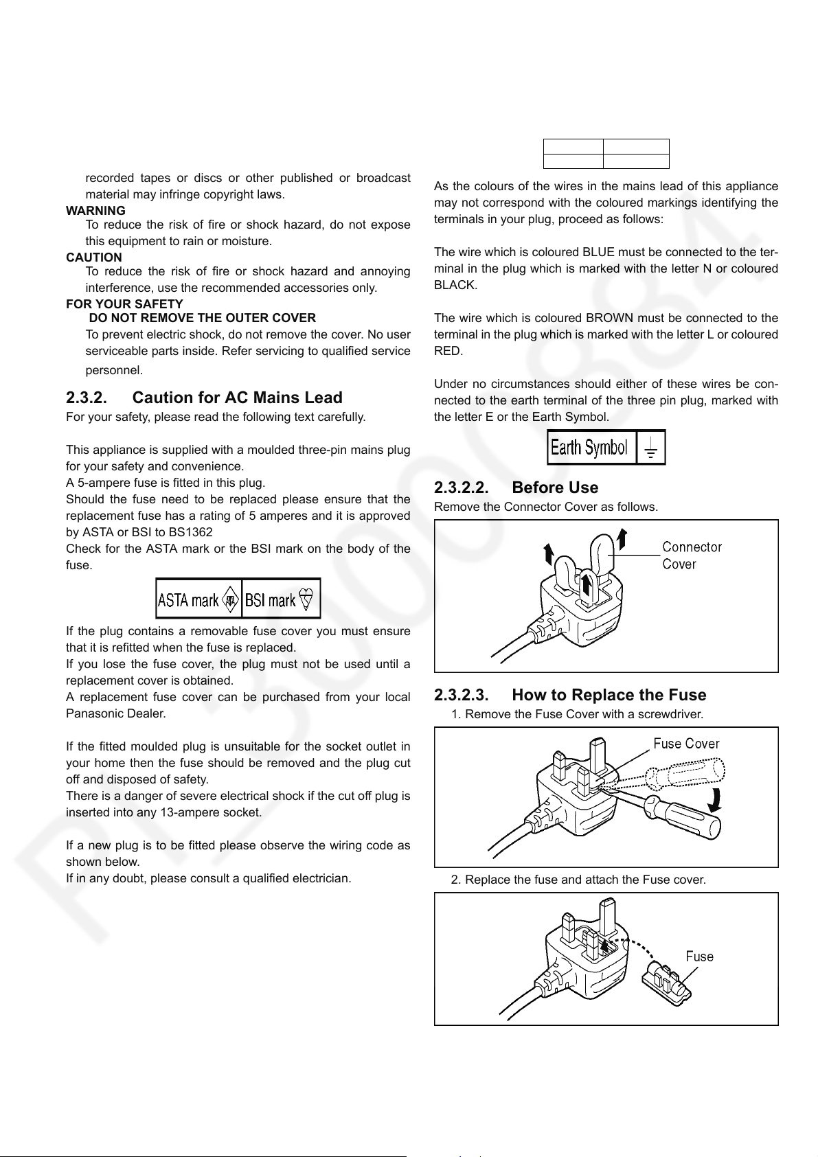
2.3.2.2. Before Use
Remove the Connector Cover as follows.
If the plug contains a removable fuse cover you must ensure
that it is refitted when the fuse is replaced.
If you lose the fuse cover, the plug must not be used until a
replacement cover is obtained.
A replacement fuse cover can be purchased from your local
Panasonic Dealer.
If the fitted moulded plug is unsuitable for the socket outlet in
your home then the fuse should be removed and the plug cut
off and disposed of safety.
There is a danger of severe electrical shock if the cut off plug is
inserted into any 13-ampere socket.
If a new plug is to be fitted please observe the wiring code as
shown below.
If in any doubt, please consult a qualified electrician.
2.3.2.3. How to Replace the Fuse
1. Remove the Fuse Cover with a screwdriver.
2. Replace the fuse and attach the Fuse cover.
5
2.4. How to Replace the Lithium Battery
2.4.1. Replacement Procedure
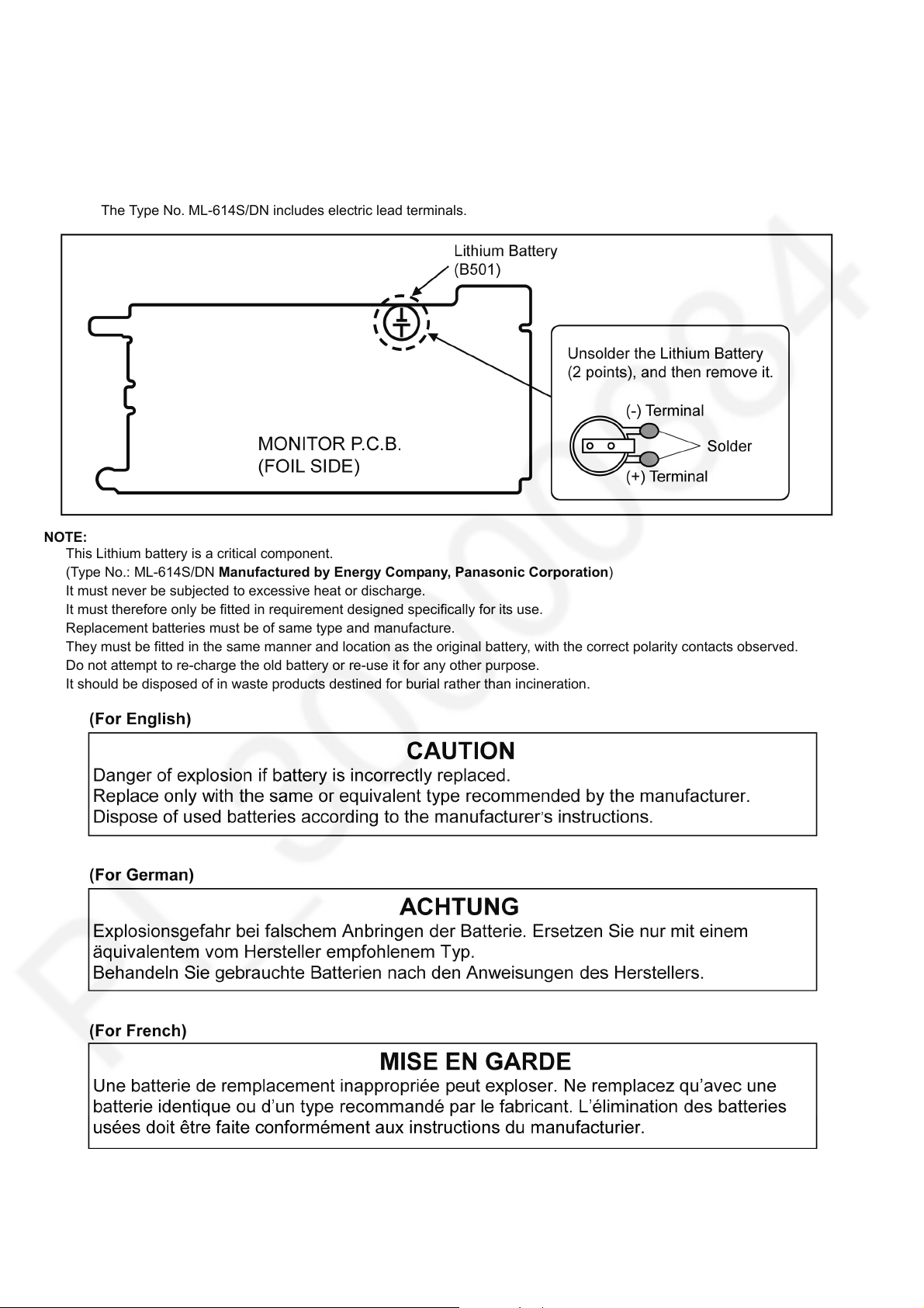
1. Remove the MONITOR P.C.B.. (Refer to Disassembly Procedures.)
2. Unsolder the each soldering point of electric lead terminal for Lithium battery (Ref. No. “B501” at foil side of MONITOR
P.C.B.) and remove the Lithium battery together with electric lead terminal. Then replace it into new one.
NOTE:
The Type No. ML-614S/DN includes electric lead terminals.
NOTE:
This Lithium battery is a critical component.
(Type No.: ML-614S/DN Manufactured by Energy Company, Panasonic Corporation)
It must never be subjected to excessive heat or discharge.
It must therefore only be fitted in requirement designed specifically for its use.
Replacement batteries must be of same type and manufacture.
They must be fitted in the same manner and location as the original battery, with the correct polarity contacts observed.
Do not attempt to re-charge the old battery or re-use it for any other purpose.
It should be disposed of in waste products destined for burial rather than incineration.
NOTE:
Above caution is applicable for a battery pack which is for HC-V270/V260 series, as well.
6
3 Service Navigation
3.1. Introduction
This service manual contains technical information, which allow service personnel’s to understand and service this model.
Please place orders using the parts list and not the drawing reference numbers.
If the circuit is changed or modified, the information will be followed by service manual to be controlled with original service manual.
3.2. General Description About Lead Free Solder (PbF)
The lead free solder has been used in the mounting process of all electrical components on the printed circuit boards used for this
equipment in considering the globally environmental conservation.
The normal solder is the alloy of tin (Sn) and lead (Pb). On the other hand, the lead free solder is the alloy mainly consists of tin
(Sn), silver (Ag) and Copper (Cu), and the melting point of the lead free solder is higher approx.30°C (86°F) more than that of the
normal solder.
Distinction of P.C.B. Lead Free Solder being used
Service caution for repair work using Lead Free Solder (PbF)
• The lead free solder has to be used when repairing the equipment for which the lead free solder is used.
(Definition: The letter of “PbF” is printed on the P.C.B. using the lead free solder.)
• To put lead free solder, it should be well molten and mixed with the original lead free solder.
• Remove the remaining lead free solder on the P.C.B. cleanly for soldering of the new IC.
• Since the melting point of the lead free solder is higher than that of the normal lead solder, it takes the longer time to melt the
lead free solder.
• Use the soldering iron (more than 70W) equipped with the temperature control after setting the temperature at 350±30°C
(662±86°F).
Recommended Lead Free Solder (Service Parts Route.)
• The following 3 types of lead free solder are available through the service parts route.
SVKZ000001-----------(0.3mm 100g Reel)
SVKZ000002-----------(0.6mm 100g Reel)
SVKZ000003-----------(1.0mm 100g Reel)
Note
* Ingredient: tin (Sn) 96.5%, silver (Ag) 3.0%, Copper (Cu) 0.5% (Flux cored)
7
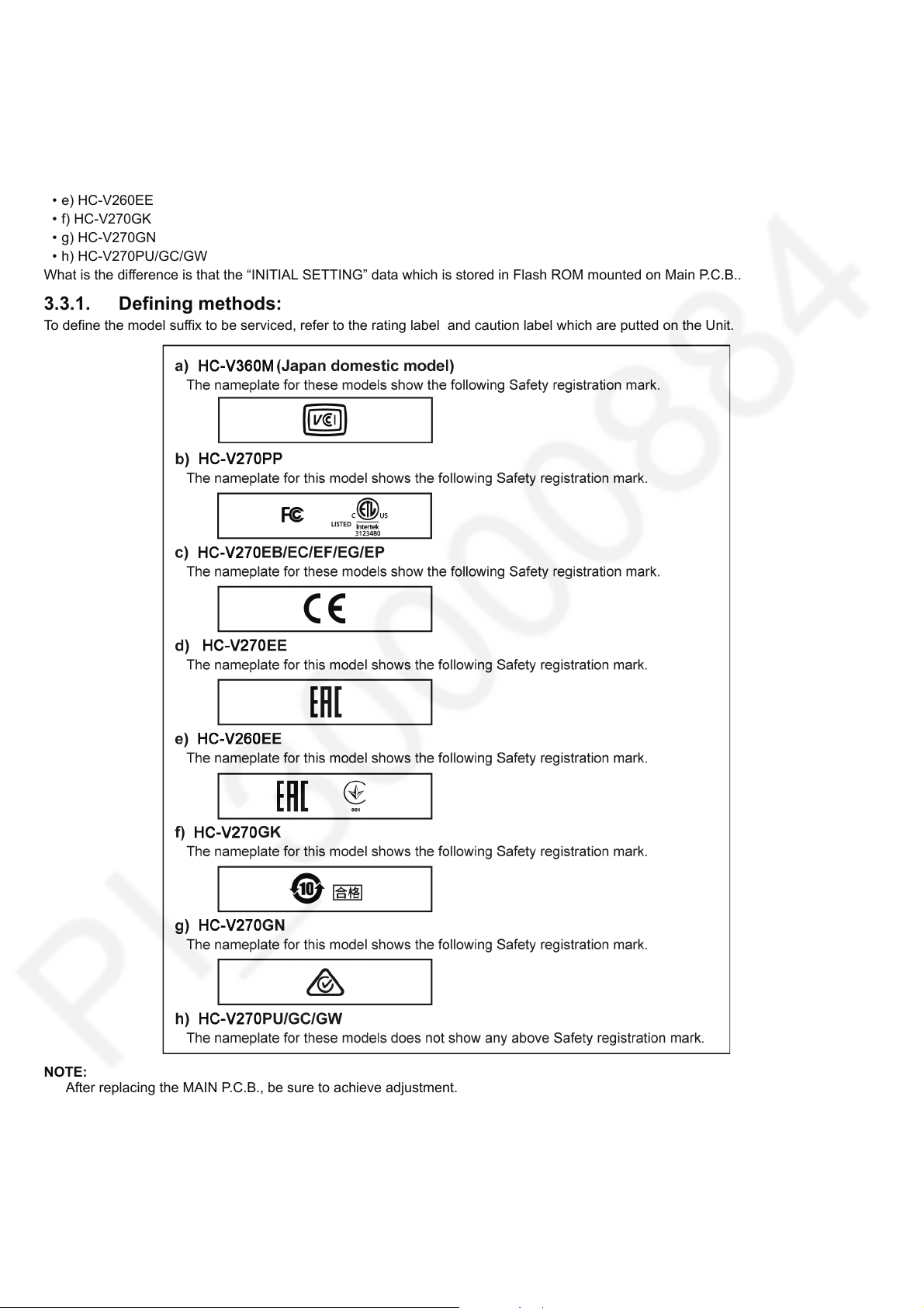
3.3. How to Define the Model Suffix (NTSC or PAL model)
There are eight kinds of HC-V270/V260.
• a) HC-V360M (Japan domestic model)
• b) HC-V270PP
• c) HC-V270EB/EC/EF/EG/EP
• d) HC-V270EE
• e) HC-V260EE
• f) HC-V270GK
• g) HC-V270GN
• h) HC-V270PU/GC/GW
What is the difference is that the “INITIAL SETTING” data which is stored in Flash ROM mounted on Main P.C.B..
3.3.1. Defining methods:
To define the model suffix to be serviced, refer to the rating label and caution label which are putted on the Unit.
NOTE:
After replacing the MAIN P.C.B., be sure to achieve adjustment.
8
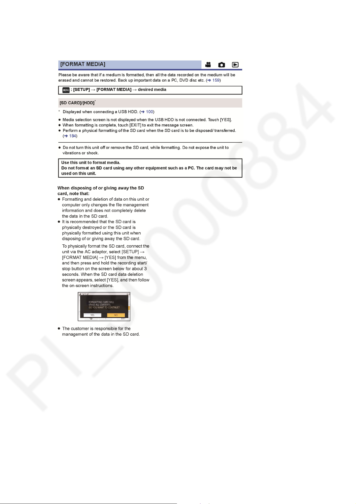
3.4. Formatting
The following formatting is for HC-V270PP.
The page number in this page does not show the page number of this service manual.
9
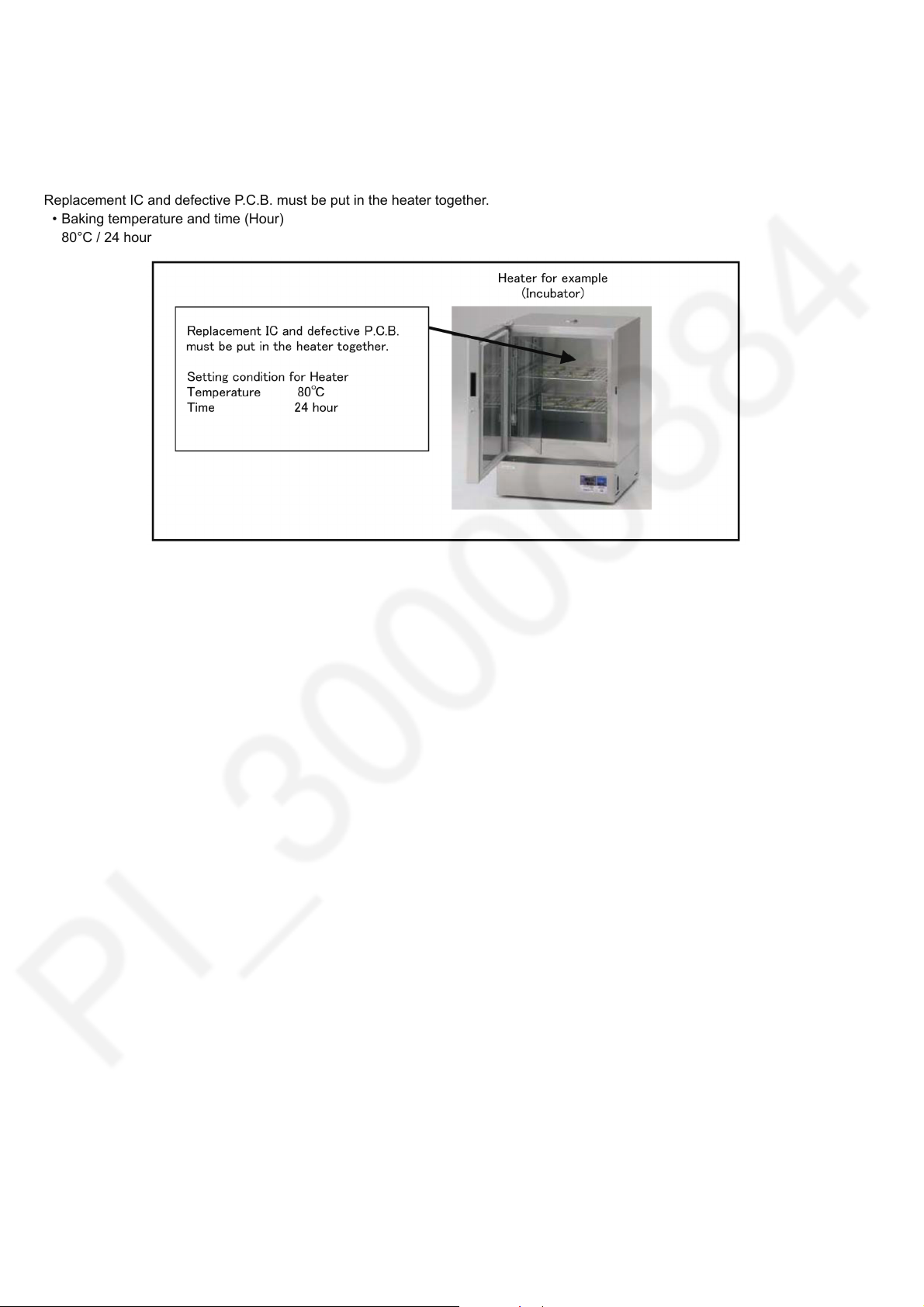
3.5. Baking of replacement IC and defective P.C.B.
When replacing the CSP/BGA/QFN type IC mounted on the P.C.B., the problem of IC crack or foil pattern breaking in the P.C.B.
might sometimes occur by rapid heating.
In order to improve the success rate of IC replacement for repair, it would be required to work out baking of replacement
IC and defective P.C.B. before replacing IC.
Please refer the way of baking as follows.
Replacement IC and defective P.C.B. must be put in the heater together.
• Baking temperature and time (Hour)
80°C / 24 hour
10
4 Specifications
The following specification is for HC-V270PP.
Some specifications may differ depending on model suffix.
The page number in this chapter does not show the page number of this service manual.
11
12
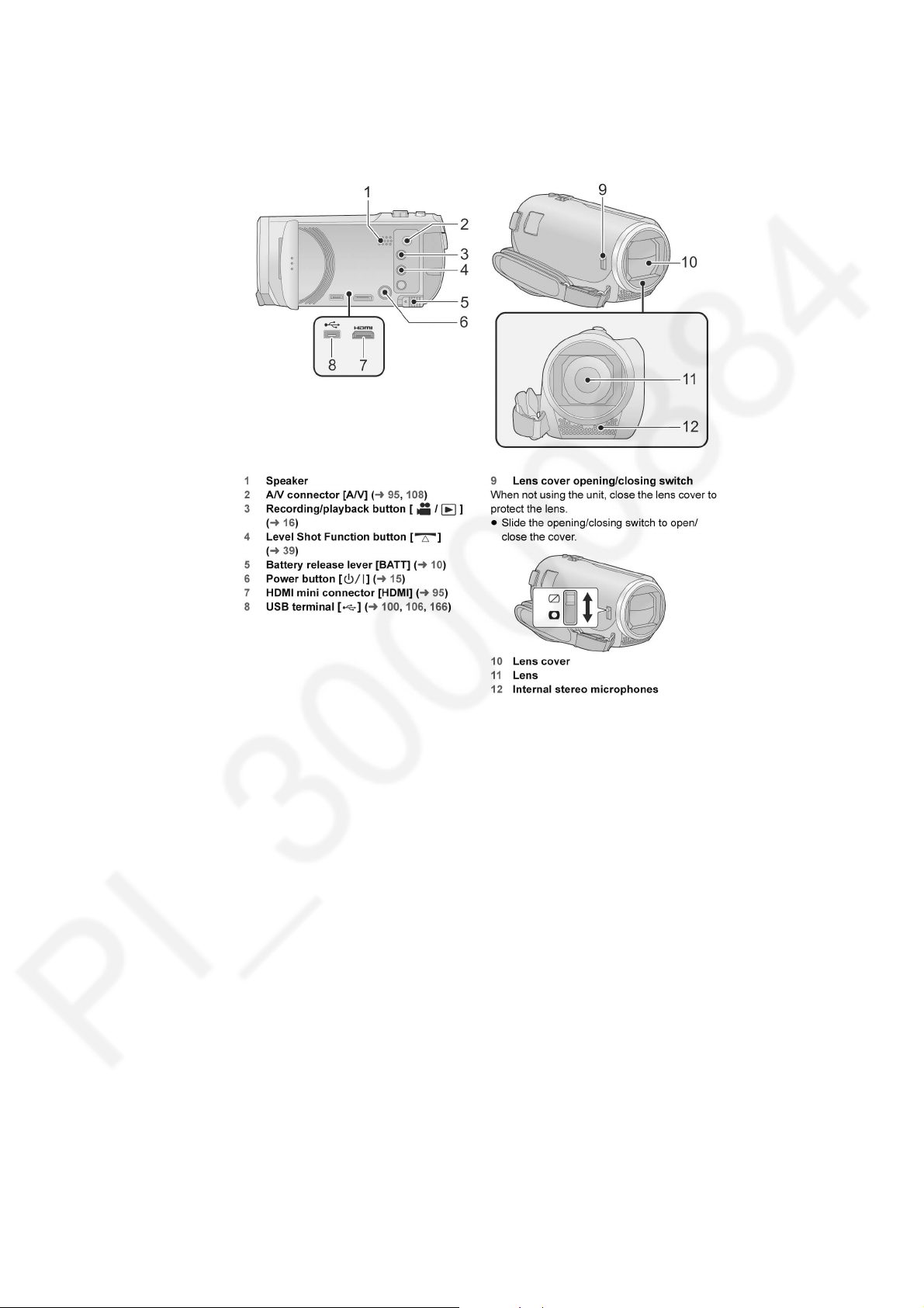
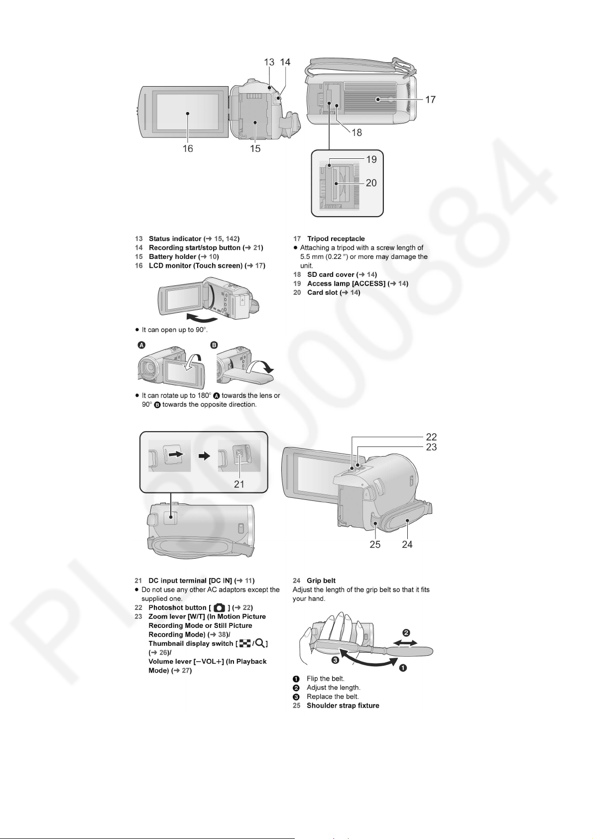
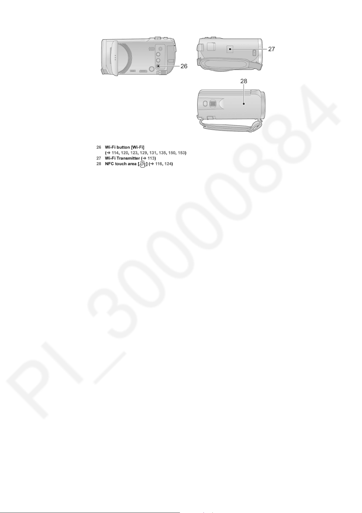
5 Location of Controls and Components
The following description is for HC-V270PP.
Some descriptions may differ depending on model suffix.
The page number in this chapter does not show the page number of this service manual.
13
141516
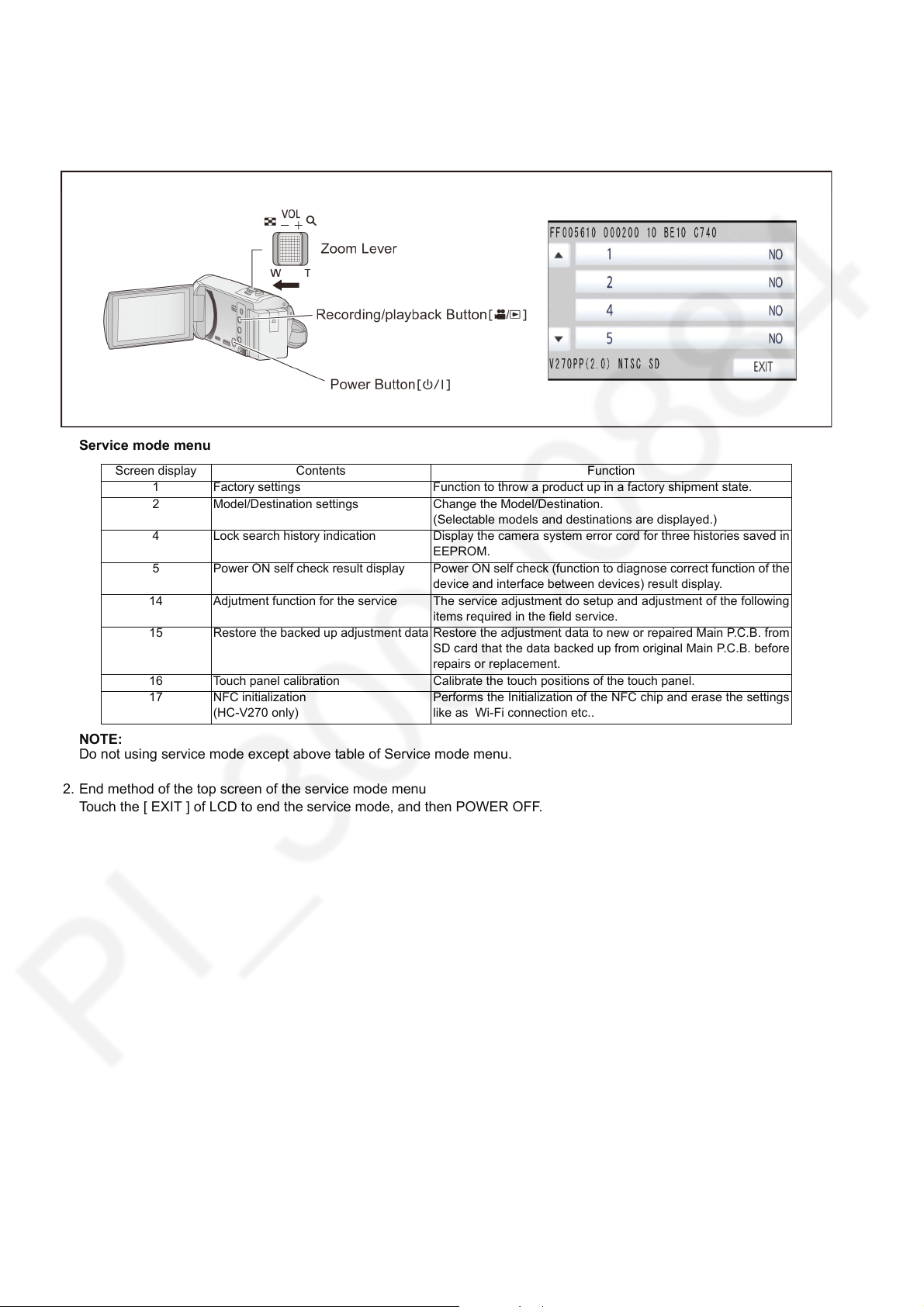
6 Service Mode
Indication method of the service menu
1. Keep pressing the “Power” button, “Zoom lever” to W side and “Recording/Playback” button for more than 3 seconds until the
top screen of the Service Mode Menu being displayed.
Service mode menu
Screen display Contents Function
1 Factory settings Function to throw a product up in a factory shipment state.
2 Model/Destination settings Change the Model/Destination.
4 Lock search history indication Display the camera system error cord for three histories saved in
5 Power ON self check result display Power ON self check (function to diagnose correct function of the
14 Adjutment function for the service The service adjustment do setup and adjustment of the following
15 Restore the backed up adjustment data Restore the adjustment data to new or repaired Main P.C.B. from
16 Touch panel calibration Calibrate the touch positions of the touch panel.
17 NFC initialization
(HC-V270 only)
(Selectable models and destinations are displayed.)
EEPROM.
device and interface between devices) result display.
items required in the field service.
SD card that the data backed up from original Main P.C.B. before
repairs or replacement.
Performs the Initialization of the NFC chip and erase the settings
like as Wi-Fi connection etc..
NOTE:
Do not using service mode except above table of Service mode menu.
2. End method of the top screen of the service mode menu
Touch the [ EXIT ] of LCD to end the service mode, and then POWER OFF.
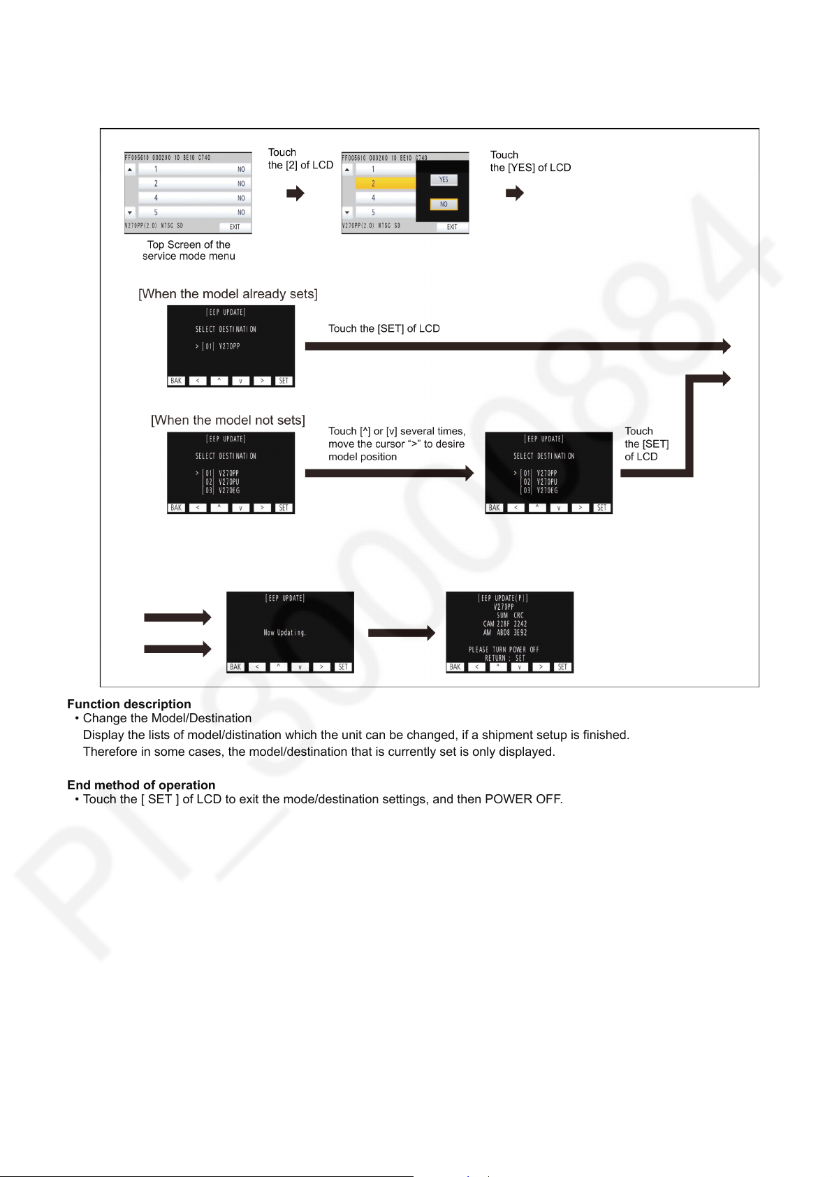
6.1. Model/Destination Settings
Touch the [ 2 ] of LCD, select model/destination settings.
Operation specifications
Function description
• Change the Model/Destination
Display the lists of model/distination which the unit can be changed, if a shipment setup is finished.
Therefore in some cases, the model/destination that is currently set is only displayed.
End method of operation
• Touch the [ SET ] of LCD to exit the mode/destination settings, and then POWER OFF.
17
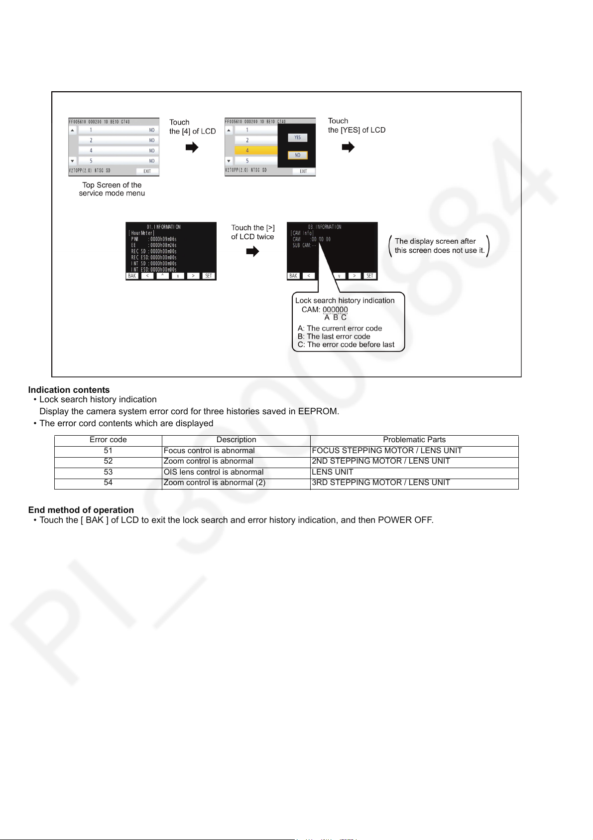
6.2. Lock Search and Error History Indication
Touch the [ 4 ] of LCD, select Lock search and error history indication.
Operation specifications
Indication contents
• Lock search history indication
Display the camera system error cord for three histories saved in EEPROM.
• The error cord contents which are displayed
Error code Description Problematic Parts
51 Focus control is abnormal FOCUS STEPPING MOTOR / LENS UNIT
52 Zoom control is abnormal 2ND STEPPING MOTOR / LENS UNIT
53 OIS lens control is abnormal LENS UNIT
54 Zoom control is abnormal (2) 3RD STEPPING MOTOR / LENS UNIT
End method of operation
• Touch the [ BAK ] of LCD to exit the lock search and error history indication, and then POWER OFF.
18
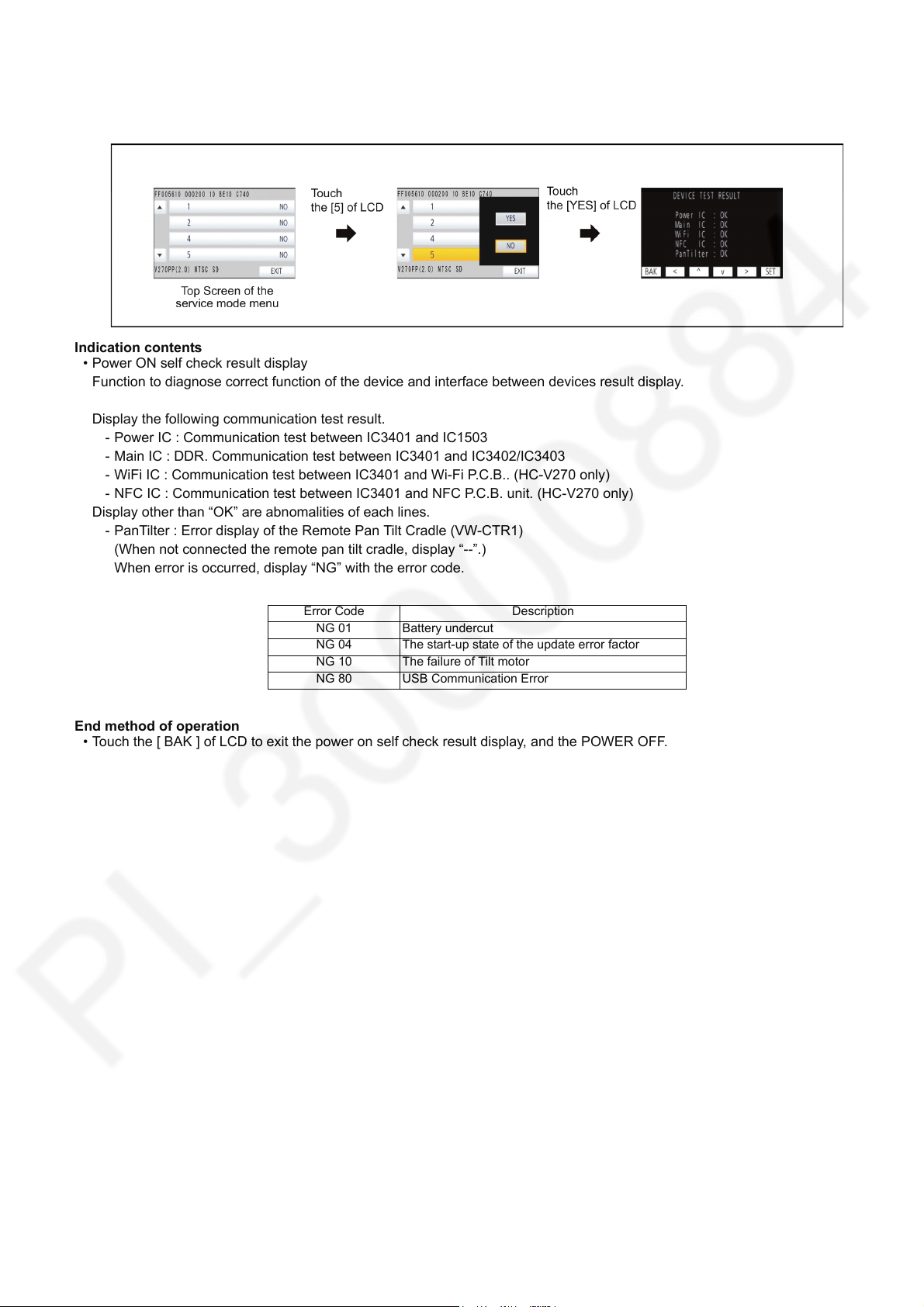
6.3. Power ON Self Check Result Display
Touch the [ 5 ] of LCD, select Power ON self check result display.
Operation specifications
Indication contents
• Power ON self check result display
Function to diagnose correct function of the device and interface between devices result display.
Display the following communication test result.
- Power IC : Communication test between IC3401 and IC1503
- Main IC : DDR. Communication test between IC3401 and IC3402/IC3403
- WiFi IC : Communication test between IC3401 and Wi-Fi P.C.B.. (HC-V270 only)
- NFC IC : Communication test between IC3401 and NFC P.C.B. unit. (HC-V270 only)
Display other than “OK” are abnomalities of each lines.
- PanTilter : Error display of the Remote Pan Tilt Cradle (VW-CTR1)
(When not connected the remote pan tilt cradle, display “--”.)
When error is occurred, display “NG” with the error code.
Error Code Description
NG 01 Battery undercut
NG 04 The start-up state of the update error factor
NG 10 The failure of Tilt motor
NG 80 USB Communication Error
End method of operation
• Touch the [ BAK ] of LCD to exit the power on self check result display, and the POWER OFF.
19

6.4. Adjustment function for the Service
Touch the [14] of LCD, select the adjustment function for the service.
Operation Specifications (until before the start of the adjustment)
Function description
The service adjustment do setup and adjustment of the following items required in the field service.
For a detailed content, such as the adjustment procedure, refer to “9 Measurements and Adjustments”.
• Model setting
• Setting of the file name for adjustment data backup to SD card.
• Execution of adjustment data backup to SD card
• Checking of Switches
• Camera adjustment
• Zoom Tracking adjustments
• Indoor White Balance Adjustment
• Outdoor White Balance Adjustment
End method of operation
• Press the power button to turn the unit off.
20

6.5. Restore the backed up adjustment data
Touch the [15] of LCD, select restoring the backed up adjustment data from SD card to the unit.
Operation Specifications
Function description
Restore the adjustment data to new or repaired Main P.C.B. from SD card that the data backed up from original Main P.C.B.
before repairs or replacement.
To backup the adjustment data, use “6.4. Adjustment function for the Service”.
Restoring procedure
End method of operation
• Press the power button to turn the unit off.
21

6.6. Touch Panel Calibration
Touch the [16] of LCD, select the calibration of touch panel.
Operation Specifications
Function description
Calibrate the touch positions of the touch panel.
End method of operation
• Press the power button to turn the unit off.
6.7. NFC Initialization (HC-V270 only)
Touch the [17] of LCD, select initialization of NFC (Near Field Communication) function.
Operation Specifications
Function description
This function performs the Initialization of the NFC chip and erase the settings like as Wi-Fi connection etc..
End method of operation
• Press the power button to turn the unit off.
22

7 Service Fixture & Tools
7.1. Service Fixture and Tools
The following Service Fixture and tools are used for checking and servicing this unit.
Parts name Parts No. Remarks
Zoom Guide Shaft VMS8231 2 use
(* When Installing the MOS Unit )
7.2. When Replacing the Main P.C.B.
After replacing the MAIN P.C.B., be sure to achieve adjustment.
7.3. Service Position
This Service Position is used for checking and replacing parts. Use the following Extension cables for servicing.
No. Parts No. Connection Form
1 RFKZ0354 FP6001(MAIN) - MONITOR FPC 37PIN 0.3 FFC
2 RFKZ0444 PP6001(MAIN) - PS6401(SD HOLDER) 50PIN 0.5 B to B
3 VFK1480 FP6003(MAIN) - ECM FPC 6PIN 0.5 FFC
4 VFK1440 FP6402(SD HOLDER) - TOP OPERATION 10PIN 0.5 FFC
7.3.1. Extention Cable Connection
23

8 Disassembly and Assembly Instructions
8.1. Disassembly Flow Chart for the Unit
This is a disassembling chart.
When assembling, perform this chart conversely.
24
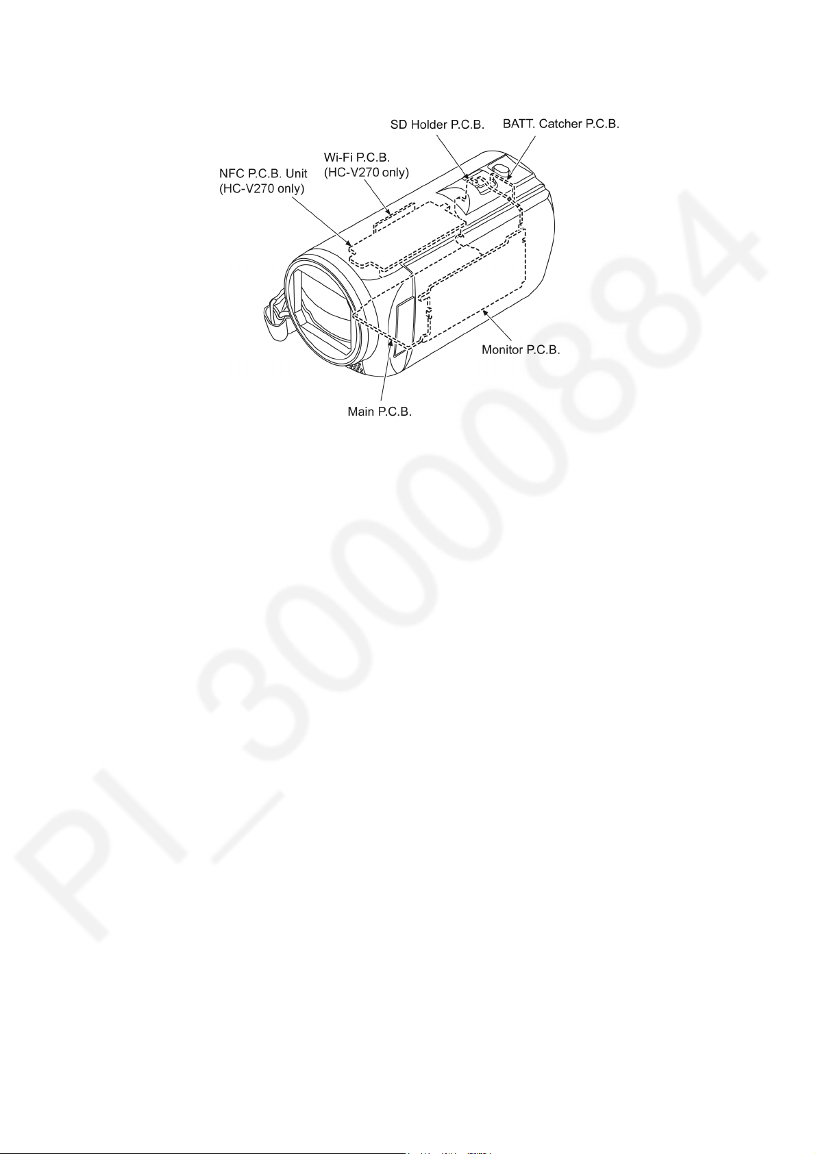
8.2. PCB Location
25

8.3. Disassembly Procedure for the Unit
No. Item Fig Removal
1 Side Case-L Unit (Fig. D1) Screw (A) x 3
(Fig. D2) Screw (B) x 1
Locking tab x 3
Hooking part x 3
Side Case-L Unit
2 Top Case Unit,
Power Panel Light,
LED Piece,
Jack Cover Piece,
Jack Cover Spring,
SS Button, SS Lever,
Jack Cover Unit
3 Front Case Unit (Fig. D4) Screw (E) x 1
4NFC P.C.B. Unit
(HC-V270 only)
5Wi-Fi P.C.B.
(HC-V270 only)
6 Lens Frame Unit (Fig. D8) Screw (J) x 1
7 Camera Lens Unit (Fig. D10) FP301 (Flex)
8Main P.C.B.,
SD Holder P.C.B.
(Fig. D3) Screw (C) x 1
Locking tab x 3
Top Case Unit
Power Panel Light
LED Piece
Screw (D) x 1
Convex x 1
Hooking part x 1
Jack Cover Piece
Jack Cover Spring
SS Button
SS Lever
Jack Cover Unit
Screw (F) x 2
FP6003 (Flex)
Screw (G) x 1
Convex x 2
(Fig. D5) Front Case Unit
(Fig. D6) Screw (H) x 1
FP6006 (Flex)
Hooking part x 1
NFC P.C.B. Unit
(Fig. D7) Flex A
Screw (I) x 1
Wi-Fi P.C.B.
Hooking part x 2
Heat Radiation Plate-L Unit
Screw (K) x 1
P6003 (Connector)
Screw (L) x 1
Convex x 2
Locking tab x 2
(Fig. D9) Lens Frame Unit
FP6008 (Flex)
Convex x 2
Camera Lens Unit
(Fig. D11) Screw (M) x 1
Screw (N) x 3
Screw (O) x 1
Convex x 2
Hooking part x 1
Heat Radiation Plate Unit
P6401 (Connector)
FP6001 (Flex)
FP6402 (Flex)
(Fig. D12) Convex x 5
Locking tab x 4
Bottom Frame Unit
Main P.C.B.
SD Holder P.C.B.
No. Item Fig Removal
9 Top Operation,
BATT. Catcher P.C.B.
10 R Frame Unit,
Speaker,
LCD Unit
11 Monitor P.C.B.,
LCD Hinge Unit,
Light Guide Plate Unit,
LCD Panel Unit
12 Spring Holder,
Barrier Lever
13 Front Base,
Barrier R,
Barrier F
14 Front Case,
Mic Cover,
Front Ornament Ring,
Flare Cut Piece,
Microphone Unit
15 MOS Unit,
IR Cut Grass
(Fig. D13) Convex x 1
Hooking part x 1
Locking tab x 1
Top Operation
Hooking part x 1
BATT. Catcher P.C.B.
(Fig. D14) Screw (P) x 2
Locking tab x 4
R Frame Unit
Convex x 1
LCD Lever
(Fig. D15) Convex x 2
Convex x 6
Speaker
Convex x 2
LCD Unit
(Fig. D16) Screw (Q) x 2
Locking tab x 9
LCD Case (T) Unit
Screw (R) x 1
FP901 (Flex)
FP904 (Flex)
FP905 (Flex)
(Fig. D17) Locking tab x 1
Hooking part x 1
Monitor P.C.B.
LCD Hinge Unit
LCD Frame A
Locking tab x 4
Light Guide Plate Unit
LCD Panel Unit
(Fig. D18) Reflection Sheet
Light Guide Plate
Diffusion Sheet
Prism Sheet (B)
Prism Sheet (A)
LGP Holder
(Fig. D19) Screw (S) x 1
Spring Holder
Barrier Spring
Locking tab x 2
Barrier Lever
(Fig. D20) Projection part x 3
Lens Damper Rubber
Screw (T) x 4
Convex x 3
Front Base
Barrier R
Barrier F
(Fig. D21) Screw (U) x 2
Locking tab x 1
Front Case
Mic Cover
Front Ornament Ring
Flare Cut Piece
Mic Sponge-F
Mic Sponge-M
Microphone Unit
Mic Sponge-R
(Fig. D22) Screw (V) x 3
MOS Unit
MOS Cushion
IR Cut Grass
(Fig. D23) NOTE: (When Installing
(Fig. D24)
the MOS Unit)
26

No. Item Fig Removal
16 2nd Stepping Motor (Fig. D25) Solder x 16 points
Screw (W) x 3
Convex x 5
(Fig. D26) Screw (X) x 2
2nd Stepping Motor
17 3rd Stepping Motor (Fig. D27) Solder x 4 points
Screw (Y) x 1
Convex x 1
(Fig. D28) Screw (Z) x 2
3rd Stepping Motor
18 Focus Motor (Fig. D29) Solder x 8 points
Screw (a) x 1
Convex x 1
(Fig. D30) Screw (b) x 2
Focus Motor
27
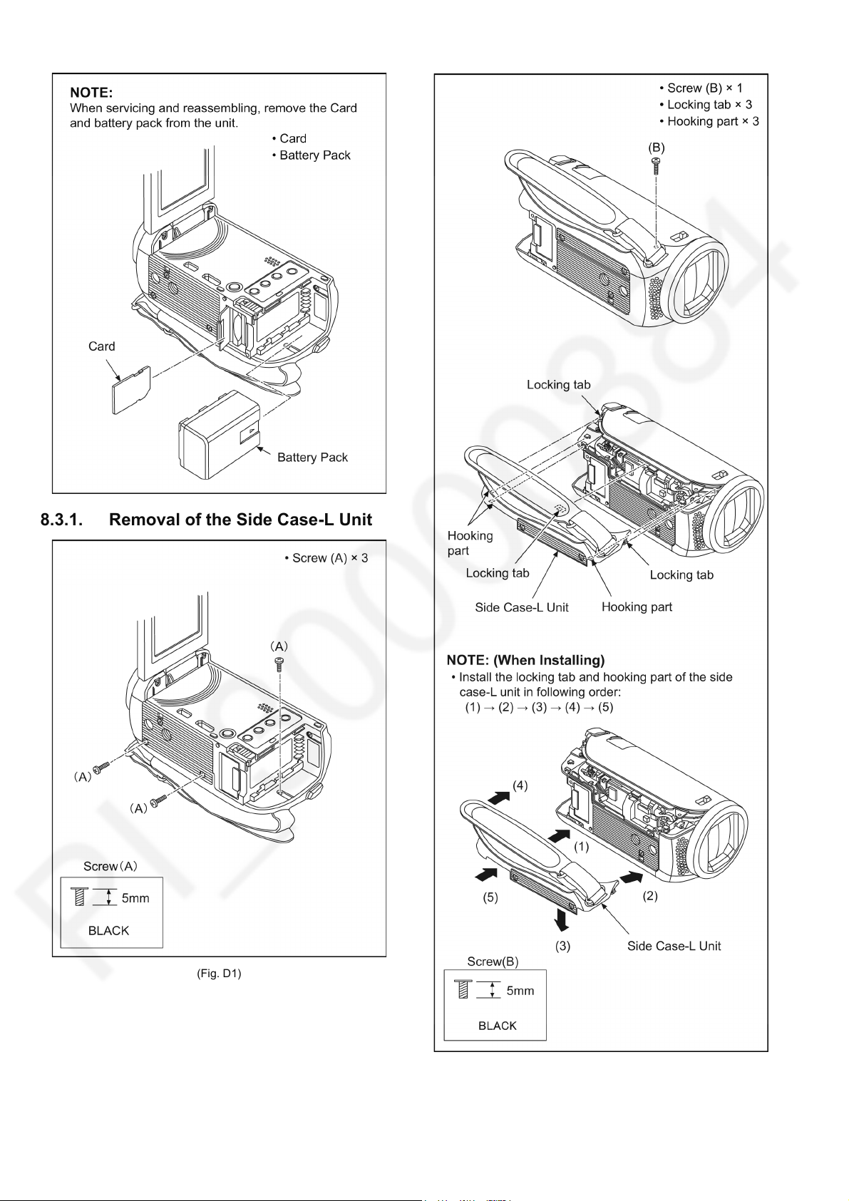
8.3.1. Removal of the Side Case-L Unit
(Fig. D1)
(Fig. D2)
28

8.3.2. Removal of the Top Case Unit, Power Panel Light, LED Piece, Jack Cover Piece, Jack Cover Spring, SS Button, SS Lever, Jack Cover Unit
8.3.3. Removal of the Front Case Unit
(Fig. D3)
(Fig. D4)
29

(Fig. D5)
8.3.4. Removal of the NFC P.C.B. Unit (HC-V270 only)
8.3.5. Removal of the Wi-Fi P.C.B. (HCV270 only)
(Fig. D6)
(Fig. D7)
30

8.3.6. Removal of the Lens Frame Unit
(Fig. D9)
(Fig. D8)
31

8.3.7. Removal of the Camera Lens Unit
8.3.8. Removal of the Main P.C.B., SD Holder P.C.B.
(Fig. D10)
(Fig. D11)
32

8.3.9. Removal of the Top Operation, BATT. Catcher P.C.B.
(Fig. D12)
(Fig. D13)
33

8.3.10. Removal of the R Frame Unit, Speaker, LCD Unit
(Fig. D14)
(Fig. D15)
34
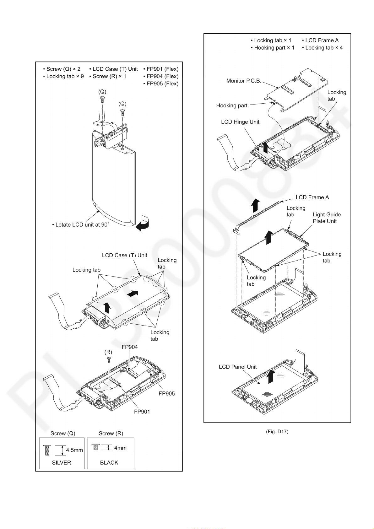
8.3.11. Removal of the Monitor P.C.B., LCD Hinge Unit, Light Guide Plate Unit, LCD Panel Unit
(Fig. D16)
(Fig. D17)
35

8.3.12. Removal of the Spring Holder, Barrier Lever
(Fig. D18)
(Fig. D19)
36

8.3.13. Removal of the Front Base, Barrier R, Barrier F
8.3.14. Removal of the Front Case, Mic Cover, Front Ornament Ring, Flare Cut Piece, Microphone Unit
(Fig. D20)
(Fig. D21)
37

8.3.15. Removal of the MOS Unit, IR Cut Grass
(Fig. D22)
38
(Fig. D23)

(Fig. D24)
8.3.16. Removal of the 2nd Stepping Motor
39
(Fig. D25)

8.3.17. Removal of the 3rd Stepping Motor
(Fig. D26)
(Fig. D27)
40

8.3.18. Removal of the Focus Motor
(Fig. D28)
(Fig. D29)
41

(Fig. D30)
42

9 Measurements and Adjustments
9.1. Electric Adjustment
• Adjustment method is different from a conventional High definition video camera.
• An exclusive jig are necessary for electric adjustment.
• Connection method of the main unit and an exclusive adjustment jig as follows.
Figure of connection
Figure of image when adjustment
43

Part Number of jig
1. Basic Jig
Item Contents
AC adaptor Bandled with camcorder
AC Cable Bandled with camcorder
2. Optical Jig for Camera Adjustment
Item Part number Remarks
Light box VFK1164TDVLB/RFKZ0523* Need external power supply: 12V ± 0.1V /1.8A or over
Collimator with focus chart VFK1164TCM02/VFK1164TCM03 Same as DSC
CC filter 3100K/5100K VFK1164CC10G Need 2 set. For indoor/outdoor white balance adjutment
C2 Filter 5100K VFK1164LBB2 For outdoor white balance adjustment
C8 Filter 5100K VFK1164LBB8 For outdoor white balance adjustment
ND Filter 0.1 3100K VFK1164ND01 For indoor white balance adjustment
ND Filter 0.6 3100K VFK1164ND06 For indoor white balance adjustment
* RFKZ0523 (same as DSC) is recommended.
44

9.1.1. About Light Box
When using VFK1164TDVLB Light Box
If using VFK1164TDVLB Light Box, remove the lens connection ring by loosing thumbscrew and three hexagon screws.
* RFKZ0523 Light Box has no lens connection ring.
How to remove the Front Hood
In order to utilize maximum of the diffusing surface of light box, some adjustment items need the distance between diffusing
surface of light box and camera body becomes several cent-meters.
Before the adjustments, remove the front hood of light box following steps below.
[ For VFK1164TDVLB Light Box ]
[ For RFKZ0523 Light Box ]
45

9.1.2. Adjustment Items
Adjustment item as follows.
46

9.1.3. Adjustment Procedure
All adjustments except “Touch Panel Calibration”, “Factory Setting” and “NFC Initialization” performs using “14 Adjustment function
for the service” in service mode menu.
“Touch Panel Calibration” is performed using 16 of service mode menu and “Factory Setting” is performed using 1, “NFC Initialization” is performed using 17 of service mode menu. Refer to “6 Service mode” and “10 Factory Setting”.
[Execute adjustment function for service]
1. While the power is turned OFF, keep pressing the “Power” button, “Zoom lever” to W side and “Recording/Playback” button
for more than 3 seconds until the top screen of the Service Mode Menu being displayed.
2. Touch the twice then touch the [14] of LCD.
3. Touch the [YES] of LCD.
47

[Adjustment Procedure]
Adjustments and settings are performed following order:
1. Model setting
2. Filename setting for backup to SD card
3. Backing up adjustment data to SD card
4. Checking switches
5. Camera adjustment
6. Zoom/tracking adjustment
7. Indoor white balance adjustment
8. Outdoor white balance adjustment
48

49505152535455


10 Factory Setting
10.1. How To Turn On The Factory Settings?
1. While the power is turned OFF, keep pressing the “Power” button, “Zoom lever” to W side and “Recording/Playback” button for
more than 3 seconds until the top screen of the Service Mode Menu being displayed.
2. Touch the [ 1 ] of LCD.
3. Touch the [ YES ] of LCD.
4. After few seconds “END” is displayed on LCD monitor. Cutting of battery connection or AC power supply connection as a
completion of the “FACTORY SETTINGS”.

10.2. What Is The Factory Settings?
The factory settings clean up and/or refresh the following settings.
1. Setting values of menu.
2. Clear the time and date setting.
3. Initialize the Wi-Fi data settings (HC-V270 only)
4. Initialize the NFC data settings (HC-V270 only)
The setting position of factory settings:
Name Setting position
Lens Barrier Open
56

11 Block Diagram
HC-V20/V20 OVERALL BLOCK DIAGRAM
IC705
STEPPING MOTOR
DRIVE
NOTE
: VIDEO SIGNAL
: AUDIO SIGNAL
: CLK or CONTROL LINE
IRIS
LENS(F1.8-4.2 50x)
IC701
LENS/OIS/MOTOR DRIVE
SD
CARD
SPEAKER
ECM
OPERATION
TOUCH PANEL
DC IN
BATTERY
MOS IMAGE
SENSOR
A/V
TERMINAL
HDMI mini
CONNECTOR
ZOOM/
FOCUS
MOTOR/
OIS
Analog
Analog
Analog
Analog
IC6401
GYRO
SENSOR
(PIT/YAW)
IC3404
NAND
FLASH ROM/
1Gbit
IC3402,3403
DDR3 SDRAM/
1Gbit
IC3401
VENUS ENGINE
IC1001
POWER
LED LIGHT
X3402
OSC
(60MHz)
IC302
GA
TE IC
COLOR LCD
PANEL
IC3701
AVIO
X2303
(32.768kHz)
IC1503
RTC/CHARGE/
POWER CONTROL
USB TERMINAL
IC301,703,704
REGULATOR
IC1002,1481
REGULATOR
IC1471
POWER-DISTRIBUTION
SWITCHES
Wi-Fi
MODULE
Wi-Fi ANT.
NFC
NFC ANT.
IC2301
RESET
IC1501
REGULATOR
NFC P.C.B. UNIT
HC-V20 only
HC-V20 only
Wi-Fi P.C.B.
HC-V20 only
11.1. Overall Block Diagram
57

11.2. Camera/System Control Circuit Block Diagram
HC-V20/V20 CAMERA/SYSTEM CONTROL CIRCUIT BLOCK DIAGRAM
IC3401
(VENUS ENGINE)
AF17
AE17
AD20
AC20
AF16
AE16
AF18
AE18
AF19
AE19
RL3403 RL3404
RL3401 RL3402
IC3406
(RESET)
RSTB
4
VDD
PW REG3V
2
T20
OUT
BUS240 DAP
BUS240 DAM
BUS240 DBP
BUS240 DBM
BUS240 DCP
BUS240 DCM
BUS240 DDP
BUS240 DDM
BUS240 CKP
BUS240 CKM
DOAP
DOAM
DOBP
DOBM
DOCP
DOCM
DODP
DODM
DCKP
DCKM
AE22
XVD CAM GLVD
AF22
XHD CAM
AE23
S SENS SDO
AE24
S SENS SCK
AF24
S SENS CS
VD
HD
SDI
SCK
SCS
X3402
(60MHz)
5
1
4
32
IC302
(GATE IC)
PW MOS1.8V
E NRST
(From QR2389-C)
CLK60 MOS
AF23
AF15
E MOS RST
RSTN
MCLK
MOS UNIT
X2303
(32.768kHz)
S6001
LCD OPEN
CARD LED
E KEYIN4
D6401
CARD
LED
PW REG3V
QR6402
FP905
X RIGHT
Y BOT
X LEFT
Y TOP
1
2
3
4
PW REG3V
PW REG1.8V
U25
R25
R26
P23
P24
G16
E17
E16
G15
PW REG3V
STANDBY LED B
V24
QR6401
AB13
QR3404 QR3401
QR3405
QR3402
E15
TOUCH PANEL
UNIT
IC1503
(RTC/CHARGE/POWER CONTROL)
S6002
POWER ON/OFF
D3
G5
G6
/SWIN1
E3
/SWIN2
XIN
XOUT
A5
LED
IC511
(MAGNETIC SENSOR)
4
3
1
2
VDD
OUT
GND
NC
AD TPY RIGHT
AD TPY LEFT
AD TPX TOP
SEL2 ON LOW
SEL2 ON HI
LCD RVS
SEL1 ON HI
SEL1 ON LOW
AD TPX BOT
B6
CS
B7
SCK
C6
SDI
C7
SDO
CH3408
QR3403
TOP OPERATION
FP6402
ZOOMAD
PHOTO1 HANOSHI
PHOTO2 ZENOSHI
8
7
10
6
5
4
POWER LED
2
STANDBY LED
AVREF
AVREF
PW REG3V
E KEYIN1
D15
S6404
S/S
S6401
Wi-Fi
S6403
MODE
S6402
OIS
●
ZOOM LEVER
●
PHOTO SHOT BUTTON
POWER LED
PW REG3V
QR6006
QR6008
QR6007
AA23
PW RTCVREG32
P LED ON L
S RTC DI
S RTC DO
S RTC SCK
RTC CS
ZSW
(To IC701-49)
S RTC DI
S RTC DO
S RTC SCK
AB25
AB24
AB26
RTC CS
W22
HC-V20 only
58

11.3. Video/Audio Signal Process(1) Circuit Block Diagram
HC-V20/V20 VIDEO/AUDIO PROCESS(1) CIRCUIT BLOCK DIAGRAM
MOS
UNIT
CAMERA SECTION
IC3401
(VENUS ENGINE)
BUS24 SDDAT2
BUS24 SDDA
T3
CLK24 SDCMD
CLK48 SDCARD
E CARD DET
E CARD PRO
BUS24 SDDAT1
BUS24 SDDAT0
7
8
9
1
2
5
10
12
D0
D1
D2
D3
CMD
CLK
C.DET
WP
11
ABCK1
VIDEOOUT
AODAT
AODAT0
AIDAT0
CLK B1
A7
B7
A5
B5
B6
A6
C5
C4
CLK 12M
CLK12 IN
L26
MEMORY CONTROL
MAIN CPU
HDMI
CONTROL
CAMERA
DSP
H.264
MPEG2
JPEG
AC3
PROCESSOR
AD25
AD26
AC26
AC25
AIDAT
CLK+
CLK-
S DO AVIO
S CLK AVIO
G VIDEO
E AVIO RST
Y14
E AVIO RST
HS3901
(SD CARD CONNECTOR)
ALRCK1 CLK LR1
AC24
S CS AVIO
U26
S CLK AVIO
AA24
S DO AVIO
AB23
S CS AVIO
CLK27 AUDIO
P26
CLK27 AVL3V
BUS24 SDDAT0-3
STREAM CONTROL
DATA2+
DATA2-
DATA1+
DATA1-
DATA0+
DATA0-
HPD
SCL
SDA
CEC
1 8
72
FL6001
2
3
3 6
54
5
6
1 8
72
FL6002
8
9
14
3 6
54
11
12
15
16
19
JK6003
HDMI MINI CONNECTOR
A16
TMDS2P
A8
D8
CEC
HPDTCT
C8
S DAT DDC
B8
S CLK DDC
B16
TMDS2N
A17
TMDS1P
B17
TMDS1N
A18
TMDS0P
B18
TMDS0N
A19
TMDSCLKP
B19
TMDSCLKN
HDMI DMA I/F
CAMERA SIGNAL PROCESSOR
AUDIO DSP
BUS240 DAP
BUS240 DAM
BUS240 DBP
BUS240 DBM
BUS240 DCP
BUS240 DCM
BUS240 DDP
BUS240 DDM
BUS240 CKP
BUS240 CKM
AF17
AE17
AD20
AC20
AF16
AE16
AF18
AE18
AF19
AE19
BUS20 FR D0
BUS20 FR D7
BUS 20 FR CLE
BUS20 FR ALE
BUS20 FR RB
BUS20 FR WP
BUS20 FR CS
BUS20 FR RE
BUS20 FR WE
G3
E4
W2
AB3
E3
A3
H1
D3
G1 G2H3H2 H4
BUS400 DCKP
BUS400 DCKN
BUS400 DCKE
BUS400 ZDCS
BUS400 ZRAS
BUS400 ZCAS
BUS400 ZDWE
BUS400 DBA2
AF4 AC5
AF3
AD4 AE4
AD7
AC6
DATA
IC3404
(NAND FLASH ROM/1G-bit)
41 48 5251 59
17
8 7 12 10 16 11
CTL SIG
IC3402/3403
(DDR3 SDRAM/1G-bit)
56 5857
BUS400 DQ0
BUS400 DQ15
AD8
BUS400 DBA1
AC9
BUS400 DBA0
AD9
DDR3 ZDRST
AD10
K7 K9J7J3 K3 L3
L2
M3 N8 M2 T2
BUS400 DQM0
Y3
BUS400 DQM1
AA3
Y2
BUS400 DQSN0
W1
BUS400 DQSP0
AC2
BUS400 DQSN1
AC1
E7 D3
G3 F3 B7 C7
BUS400 DQSP1
AE5
AF6
N3
N7
BUS400 DA0
BUS400 DA12
ADDRESSCTL SIG CTL SIG
DATA
L2
P4
E3
A3
BUS400 DQ16
BUS400 DQ31
BUS400 DQM2
M3
BUS400 DQM3
P3
M2
BUS400 DQSN2
L1
BUS400 DQSP2
R2
BUS400 DQSN3
R1
E7 D3
G3 F3 B7 C7
BUS400 DQSP3
CTL SIG
DATA
IC3402 ONLY IC3403 ONLY
A22
D20
A23
D22
C22
B22
E21
D21
C21
CLK36 LCD
A21
B21
S DO LCD
S CS LCD
BUS18 LCDYC0
BUS18 LCDYC1
BUS18 LCDYC2
BUS18 LCDYC3
BUS18 LCDYC4
BUS18 LCDYC5
BUS18 LCDYC6
BUS18 LCDYC7
BUS18 LCDH
BUS18 LCDV
C25
S CLK LCD
B24
C26
LCD
BUS18 LCDYC0-C7
BUS24 WIDAT0-3
E1
E2
C1
C2
D1
D2
CLK48 WIFI
CLK24 WICMD
BUS24 WIDAT0
BUS24 WIDAT1
BUS24 WIDAT2
BUS24 WIDAT3
E10
E WIFI RST
T22
W23
S DI NFC
U22
S DO NFC
IRQ NFC
R22
S SCK NFC
IRQ NFC2
(To IC1503-C4)
CH3411
3
4
2
USB TERMINAL
D-
D+
JK6001
A12
A13
Y17
USB D-
USB D+
USB IDDET L
ID
To VIDEO/AUDIO PROCESS(2
)
BLOCK DIAGRAM
Wi-Fi P.C.B.
NFC P.C.B. UNIT
(Wi-Fi MODULE)
Wi-Fi ANT.
(NFC)
NFC ANT.
HC-V20 only
59

11.4. Video/Audio Signal Process(2) Circuit Block Diagram
HC-V20/V20 VIDEO/AUDIO PROCESS(2) CIRCUIT BLOCK DIAGRAM
IC3701
(AVIO)
IC3702
(SINGLE CLOCK GENERATOR)
12
BICK
CLK B1
CLK LR1
AIDAT0
AODAT0
11
LRCK
24
VIN
CLKIN
OE
FSEL
CLKOUT
JK6402
(AV JACK)
VOUT
4
PLUGIN L
6
LOUT
5
ROUT
1
21
22
SPN
SPP
SPK-AMP
SPEAKER
V OUT
CLAMP LPF
14
SDTO
13
SDTI
E AVIO RST
18
PDN
10
CSN/SDA
8
CCLK/SCL
S CS AVIO
S CLK AVIO
S DO AVIO
9
CDTIO/CAD0
7
I2C
CLK12 IN
17
MCKI
16
MCKO
G VIDEO
CLK27 AVL3V
PLUG IN L
(To IC3401-P20)
25
6
4
5
3
PMV
PMSPK
PMPFIL
PMPLL
PMMICL
PMADL or PMADR
PMMICR
AUDIO
I/F
CONTROL
REGISTER
PMLO
PMBP
D/A
PLL
DVOL
SMUTE
+
+
++
31
32
1
ROUT
MIN
LOUT
LIN1
A/DHPF
MIC SENSE/
CORRECTION FUN.
HPF2
MONO/
STEREO
STEREO
EMPHASIS
MIC POWER
SUPPLY
LDO: 2.3V
4 BAND EQ
LPF
ALC
1 BAND EQ
HPF3
RUNNING
AVERAGE
CIRCUIT
EQ0
INPUT
BUFFER
PLL
OUTPUT
BUFFER
3
RIN1
4
LIN2
5
RIN2
MPWR
REGFIL
AVDD
ANALOG
BLOCK
MIC POWER,SPK-AMP,
LINE/VIDEO-OUT-AMP
6
2
27
TVDD
15
DVDD
20
29
PMMP
+
-
ECM[L]
+
-
ECM[R]
RL3705
RL3704
RL3708
RL3709
PW REG3V
PW REG1.8V
PW SPK3.2V
Q3701
PW 5V
PW REG3V
VDD
1
To VIDEO/AUDIO PROCESS(1
)
BLOCK DIAGRAM
60

HC-V20/V20 LENS DRIVE CIRCUIT BLOCK DIAGRAM
FILTER
MOS
M
3G ZOOM MOTOR
M
1
2
3
30
27
28
29
IC701
(LENS/OIS/MOTOR DRIVE)
3GZAP
3GZAN
3GZBN
3GZBP
4
39
37
36
38
ZAP
ZBP
IC3401
(VENUS ENGINE)
M
IRIS MOTOR
FP6008
FP6008
ZBN
ZAN
6
HALL
SENSOR
HALL
SENSOR
OIS UNIT
FP6008
PIT DRV+
PIT DRV-
PIT HO+
PIT HIN+
PIT HIN-
YAW DRV-
YAW DRV+
YAW HIN+
YAW HIN-
YAW HO-
11
12
13
16
15
14
17
18
22
21
20
19
PIT HO-
YAW HO+
IRM+
IRM-
FP6008
FP6008
IR HO+
IR HIN+
IR HO-
IR HIN-
HALL
SENSOR
PMP
IRHOP
76
IRHON
31
71
YMP
PHON
28
YMN
70
24
PHOP
57
PHINP
PMN
77
27
IRHINP
55
IRMP
5
IRMN
8
ZAP
14
ZAN
17
ZBN
10
ZBP
13
73
YHON
74
56
YHOP
YHINP
PW GYRO3V
GCSB
GSCK
GSI
GSO
29
23
32
3
12
HD
NSCS
SCK
SDI(V2L)
SDO(L2V)
DAC LD
NPORI
STORM HD225
S NSCS LEN
SCK LEN
SDO LEN
STORM VD60
22
VD
5
AE15
AB21
V23
W20
Y18
CH712
CH753
CH710
CH754
CH711
CH713
CH718
CH719
CH720
CH6401
CH6404
CH6415
CH6403
15
1
80
SDI LEN
S DACLD LENS
E LENS RST L
Y19
W24
Y25
CH721
CH722
PWMOUT1
PWMOUT2
(GYRO SENSOR:PIT/YAW)
11
MOSI
44
10
MISO
26
8
CSB
CL6406
CL6405
35
9
SCLK
1
VCC
7
VDD
2
GND1
4
GND2
6
GND3
IC6401
2G ZOOM ENC
3GZABS LEN
FP6008
8
35
7
34
10
3G ZLEDCONT
3G ZABS
ZABS
ZLEDCONT
Y24
V26
ZABS LEN
P25
LENS TEMP
C14
LEDCONT LEN
2G ZOOM MOTOR
3G ZOOM ENC
V25
FABS LEN
41
3GZOOM H
W25
CH725
CH726
(STEPPING MOTOR DRIVE)
3
MP1
5
MN1
10
MN2
11
MP2
9
E1
6
E2
1
STB
SYSCK
IC705
12
21
CK27M
15
INT
M
FOCUS MOTOR
FAP
FAN
FBN
FBP
26
24
23
25
FP6008
42
32
31
FLEDCONT
FABS
LENS TEMP
FOCUS ENC
Q775
AFAP
AFAN
AFBN
AFBP
40
37
33
36
CLK27 AUDIO
P26
5 1
4
3
2
IC3407
(GATE IC)
PW REG1.8V
11.5. Lens Drive Circuit Block Diagram
61

HC-V20/V20 POWER SUPPLY CIRCUIT BLOCK DIAGRAM
JK6701
1
3
4
2
+
T
D
-
JK6401
2
3
4
+
-
BATTERY
DC IN
PW NFCVDD2
PW RTCVREG32
FUSE RESISTOR:
QR1002
QR1001
QR1101
Q1501
1
2 3 4
5
6
8
7
Q1502
1
2 3 4
5
6
8
7
1 2 3
46
5
Q1503
IC3401
(VENUS ENGINE)
S RTC DI
S RTC DO
S RTC SCK
RTC CS
VBUS OCP
VBUS ON H
SW NOREG
S FG PWR SDA
S FG PWR SCL
AB25
AB24
AB26
W22
D9
MOSSENS ON H
AB14
E9
B14
R24
IC2301
(RESET)
1
2
4
3
VDD
GNDCDOUT
QR2389
QR2308
CH1105
Q1504
S BATT RXD
R23
S BATT TXD
IC1503
(RTC/CHARGE CONTROL)
VREG32
WKUP
F3
B2
USB
A1
OUT
C2
A3
USBSW
G2
VREG25
(R1271/R1503/R6001)
IC PROTECTOR:
(IP6401/IP6701)
Please check the Fuse Resistor and IC Protector
when an output voltage does not output.
IP6701
IP6401
NOREG
BATT +
1
USB TERMINAL
VBUS
JK6001
ADPSW
PWSW
A2
ADP
C1
VADP
SW
F2
E2
E7
BAT
E1
VUSB
D7
ISNS
F7
TDET
B6
CS
B7
SCK
E5
SWIN4
F4
WKUP RST
C6
SDI
C7
SDO
S6002
POWER ON/OFF
LI BATT
D3
/SWIN1
B501
G4
COINBAT
G3
DVIN
A6
CHG EN
F5
FULLSET
D2
BATSET
D1
USB EN
F6
USB WK CNT
B4
R6001
CH3408
QR3403
IC1501
(REGULATOR)
IC1471
(POWER-DISTRIBUTION
SWITCHES)
IC1481
(REGULATOR)
4
3
2
1
GND
CE
VIN
VOUT
IC1002
(SWITCHING
REGULATOR)
12
13
14
15
16
8
11109
1 2 3 4
PVCC
VCC
STB
RT
P
GND
PVCC
LX1
LX1
P GND
FB
INV
GND
VOUT
7
6
5
LX2
LX2
VOUT
PW WIFI3.2V
PW WIFI3V
1
2
3
4
6
5
CEVDD
VOUT GNDCS
NC
R1503
STB6
SCL
SDA
STB1234
VOSEL3
VOSEL4
VCC
VOSEL2
VREGA
GND
VO4
INV5
VO3
REGOUT
PGND45
HX5
LX5
LX6
LX4
HX4
PGND3
PGND3
LX3
LX3
HX36
LX21
HX36
PGND2
VO2E
LX22
HX2
PGND1
SWOUT
VO1E
LX1
INV6
VDD
INV7
LED
VO7
42 3941 3840 37 36 35 3433
1
2
3
4
5
6
7
8
9
10
32
31
30
29
28
27
26
25
24
23
22
14 15 16
17 18
19
LX720PGND67
21
11 12 13
IC1001
(POWER)
PW SPK3.2V
PW LENS3.2V
PW 3.2V
R1271
PW REG1.8V
PW REG3V
PW SD3.2V
PW 5V
PW HDM5V
D902-905
(LCD BACK LIGHT)
CH1241
CH1422
PW MOS1.8V
PW VDDR1.1V
CH1101
CH1001
CH1471
CH1002
CH1103
E NRST
T20
QR1004
QR1003
PW DDR1.5V
PW MOS1.2V
PW VID1.1V
6
5
4
3
1
2
EN
IN
OUT
/FAULT
ILIM
GND
4
5
6
3
2
1
QR1471
Q1471
D6
LCD ON H
E6
U24
PW MOS2.8V
5 4
1 32
IC301
(REGULATOR)
NC
IN
OUT
GNDCE
PW LENS1.5V
IC703
(REGULATOR)
4
3
2
1
GND
CE
VDD
VOUT
PW GYRO3V
IC704
(REGULATOR)
1
2
3
4
GND
STBY
VIN
VOUT
PW LCD3V
IC1422
(REGULATOR)
4
3
2
1
GND
CE
VIN
VOUT
HC-V20 only
HC-V20 only
11.6. Power Supply Circuit Block Diagram
62

12 Wiring Connection Diagram
HC-V270/V260 INTERCONNECTION DIAGRAM
MAIN P.C.B.
(FOIL SIDE)
:
(COMPONENT SIDE)
MONITOR P.C.B.
(FOIL SIDE)
SD HOLDER P.C.B.
(FOIL SIDE)
BATT. CATCHER P.C.B.
(FOIL SIDE)
:
(COMPONENT SIDE)
FP6003
65432
1
L MCE
L
MCE
DNG D
DNG D
R MCE
R MCE
MIC
)V8.2(DDVP
)V8.2(DDVP
)V2.3(TABV
)V2.3(TABV
DNG
DNG
DNG
2
TAD
3TAD
TSR
1291715131
11
97531
)V8.2(DDVP
)V8.2(DDVP
)V2.3(TABV
)V2.3(TABV
DMC
DNG
KLC
DNG
0TAD
1TAD
TS
R
0281614121
01
864
2
5006PF
8006PF
-NIHRI
+NIHRI
-MRI
SBAZ
CCVT&CCVCNEZ
+VRDTIP
+OHTIP
-OHTIP
-VRDWAY
-
OHWAY
+OHWAY
NBF
P
B
F
N
BZ
PBZ
SBAF
CCV CN
E
F
&G3
TNOCDELZG3
NAZG3
PAZG3
2
4
6
8
012141618102
22
42628203234363
83
+OHRI
-O
HRI
+
MRI
TNOCDELZ
PMET SNEL
-VRDTIP
-NIHTIP
+NIHTIP
+VRDWAY
+
N
IHWAY
-NIHWAY
NAF
PAF
PAZ
N
A
Z
TNOCDELF
SBAZG3
NBZG3
PBZG3
13579
11
31517191123252
72
92
13
335373
93
DNG
IDS
KCS
SCS
PDOD
DNG
MCOD
PKCD
DNG
MBOD
PAOD
DNG
KLCM
NTSR
V2.1
V8.1
V8.2
246
8
012141618102224262820323
DNG
DV
DH
DNG
MDOD
PCOD
DNG
MKCD
PBOD
DNG
MAOD
DNG
DNG
V2.1
V8.1
V8.2
13579
11
31517191123252729213
33
103PF
P6003
1
2
3
4
5
6
BATT +
BATT +
T
D
BATT -
BATT -
PP6001
E KEYIN4
D GND
SP OUT2
SP OUT1
D GND
NOREG
NOREG
NOREG
NOREG
NOREG
NOREG
D GND
D GND
PW REG3V
ZOOMAD
POWER LED
STANDBY LED
E KEYIN1
PLUGIN L
E CARD DET
PW SD3R2V
PW SD3R2V
PW SD3R2V
D GND
E CARD PRO
S GYRO CSB
S GYRO SCK
S GYRO SO
S GYRO SI
GYRO GND
PW GYRO3V
S ACL SCL
S ACL SDA
D GND
D GND
SD CMD
D GND
SD DATA2
SD DATA3
SD DATA0
SD DATA1
D GND
SD CLK
D GND
AV GND
G LOUT
G VOUT
G ROUT
AV GND
CARD LED B
25
24
23
22
21
20
19
18
17
16
15
14
13
12
11
10
9
8
7
6
5
4
3
2
1
26
27
28
29
30
31
32
33
34
35
36
37
38
39
40
41
42
43
44
45
46
47
48
49
50
FP6001
THGIRYPT D
A S
TFELYPT DA S
SVR DCL
L LBDCL WP
H LBDCL WP
DNG D
DNG D
DNG D
DCL KLC
S
V3DCL WP
DNG D
DNG D
H DCL 81SUB
DNG D
6CYDCL 81SUB4CYDCL 81SUB
2CYDCL 81SUB
0CYD
C
L 81SUB
V8R1GER WP
63432303826242220281614121
01
864
2
TOB XPT DA S
POT XPT DA S
TTABIL WP
L LBDCL WP
H LBDCL WP
DNG D
DNG D
DCL OD S
DCL SC S
V3DCL WP
DCL 6
3
KLC
V DCL 81SUB
TSR DCL E
7CYDCL 81SUB
5C
YDCL 81SUB
3CYDCL 81SUB
1CYDCL 81SUB
V8R1GER WP
7353331392725232129171
51
31
11
97531
BATTERY
1076KJ
123
4
+
T
D
-
P6701
1
2
3
4
5
6
BATT +
BATT +
T
D
BATT -
BATT -
TOP OPERATION
2046PF
01
9
8765432
1
IHSONA
H 1OTOHP
DNG
DAMOOZ
F
ERVA
IHSONEZ 2OTOHP
DEL YBDNATS
DEL REWOP
DNG
FERVA
DNG
SPEAKER
P6401
2
1
SP OUT1
SP OUT2
PS6401
4NIYEK E
D
NG D
2TUO PS
1TUO PS
D
N
G D
GERON
GERON
GERON
G
ERON
GERON
GERON
DNG D
DNG D
V3GER
WP
DAMOOZ
DEL REWOP
DEL YBDNATS
1N
IYE
K
E
L NIGULP
TED DRAC E
V2R3DS WP
V2R3DS WP
V2R3DS WP
D
N
G D
O
R
P DR
A
C
E
BSC ORYG S
KCS ORYG S
O
S
ORYG S
IS OR
YG S
DNG ORYG
V3ORYG WP
LCS LCA S
ADS LCA S
DNG D
DNG D
DM
C D
S
DNG
D
2ATAD DS
3ATA
D
DS
0ATAD DS
1ATAD DS
DNG D
KL
C DS
DNG D
DNG VA
TUOL G
TUOV G
T
UO
R G
DNG VA
B DEL DRAC
5242322212029181716151
4131
211101
987
6
54321
6272829203
13233343536373839304142434
445464748494
05
FP901
PW REG1R8V
BUS9 LCDYC0
BUS9 LCDYC1
BUS9 LCDYC2
BUS9 LCDYC3
BUS9 LCDYC4
BUS9 LCDYC5
BUS9 LCDYC6
BUS9 LCDYC7
D GND
RST/GND
BUS9 LCD H
BUS9 LCD V
D GND
CLK18 LCD
D GND
PW LCD3V/REG3V
S CS LCD
S CLK LCD
S DO LCD
D GND
D GND
D GND
D GND
PW LCDBL H
PW LCDBL L
COIN BATT+
LCD RVS
SD AD TPX TOP
S AD TPYLEFT
S AD TPX BOT
S ADTPYRIGHT
1
2
3
4
5
6
7
8
9
10
11
12
13
14
15
16
17
18
19
20
21
22
23
24
25
26
27
28
29
30
31
32
Y TOP
X LEFT
Y BOT
X RIGHT
4
3
2
1
FP905
LENS UNIT
MOS UNIT
NFC P.C.B. UNIT
Wi-Fi P.C.B.
LCD
TOUCH
PANEL
6006PF
1
2
3
4
5
6
2DDVCFN WP
V3GE
R WP
2CFN ORI
CFN OD S
CFN KCS S
DNG
FP904
2
4
6
8
10
12
14
16
18
20
22
24
26
28
30
32
34
36
38
40
1
3
5
7
9
11
13
15
17
19
21
23
25
27
29
31
33
35
37
39
41
VGH
C3N
C4N
VS
C1N
C2N
VCIX2
CXP
VCIM
VCOML
VCOM
VDDIO
VSYNC
DCLK
DB0
DB2
DB4
DB6
SDA
SCS
GND
C3P
C4P
VGL
C1P
C2P
VSS2
VCI
CXN
VCOMH
VGM
VSS1
VDDL
HSYNC
NC
DB1
DB3
DB5
DB7
SCL
RESET
LCD UNIT
Wi-Fi FFC
NFC FFC
BATT.
CATCHER WIRE
MONITOR FPC
HC-V270 only
MICROPHONE UNIT
12.1. Interconnection Diagram
63
 Loading...