

Panasonic GD93 Service Manual
Order Number: MCUK001001G8
Personal Cellular Telephone
EB-GD93
Specification
900 MHz 1800 MHz
Frequency Range Tx: 890 - 915MHz
Tx/Rx frequency separation 45 MHz 95 MHz
RF Channel Bandwidth 200 kHz
Number of RF channels 124 374
Speech coding Full rate/Half rate/Enhanced Full rate
Operating temperature -10 °C to +55 °C
Type Class 4 Handheld Class 1 Handheld
RF Output Power 2 W maximum 1 W maximum
Modulation GMSK (BT = 0.3)
Connection 8 ch/TDMA
Voice digitizing 13 kbps RPE-LTP / 13 kps ACLEP / 5.6 kps CELP /
Transmission speed 270.3 kbps
Diversity Frequency hopping
Signal Reception D ouble superheterodyne
Intermediate Frequencies 225 MHz and 45 MHz
Antenna Terminal Impedance 50 τ
Antenna VSWR <2.1 : 1
Dimensions Height: 120 mm
Volume 81 ml
Weight 80 g
Display Graphical chip on glass liquid crystal, Alphanumeric,
Illumination 4 LEDs for the LCD (7-colour)
Keys 18-key Keypad, Navigation key, Memo key.
SIM Plug-in type only
External DC Supply Voltage 5.8 V
Battery 3.7 V nominal, 650mAh, Li-Ion
Standby Battery Life
DRX 9
Conversation Battery Life
PL 7, DTX 50%
Battery life figures are dependent on network conditions.
Rx: 935 - 960 MHz
VSLEP
Width: 45 mm
Depth: 16.4 mm
16 x 4 characters + 2 lines of icons.
8 LEDs for the keypad (Green)
1 LED Incoming call (Green)
1 Charging LED (Red)
170 hrs maximum
210 minutes
Tx: 1710 - 1785 MHz
Rx: 1805 - 1880 MHz
WARNING
This service information is designed for experienced repair technicians only and is not designed for use by the general public. It does not
contain warnings or cautions to advise non-technical individuals of potential dangers in attempting to service a product.
Products powered by electricity should be serviced or repaired only by experienced professional technicians. Any attempt to service or
repair the product or products dealt with in this service manual by anyone else could result in serious injury or death.
© 2000 Matsushita Communication Industrial UK
Ltd. All rights reserved. Unauthorized copying and
distribution is a violation of law.
Issue 1
Revision 0

Company Liability
This Technical Guide is copyright and issued on the strict understanding that it is not be reproduced, copied, or disclosed to
any third party, either in whole or in part, without the prior written consent of Matsushita Communication Industrial UK Ltd.
Every care has been taken to ensure that the contents of this manual give an accurate representation of the equipment.
However, Matsushita Communication Industrial UK Ltd. accepts no responsibility for inaccuracies which may occur and
reserves the right to make changes to specification or design without prior notice.
The information contained in this manual and all rights in any designs disclosed therein, are and remain the exclusive property
of Matsushita Communication Industrial UK Ltd.
Other patents applying to material contained in this publication:
BULL CP8 PATENTS
Comments or correspondence concerning this manual should be addressed to:
Customer Support Department,
Matsushita Communication Industrial UK Ltd.,
Colthrop, Thatcham,
Berkshire, RG19 4ZD.
ENGLAND
© 2000 Matsushita Communication Industrial UK Ltd.
Issue 1 - ii - MCUK001001G8
Revision 0 Techni c a l G uide

CONTENTS
1 INTRODUCTION
1.1 Purpose of this Guide . . . . . . . . . . . . . . . . . . . . . . . . . . . 1
1.2 Structure of the Guide . . . . . . . . . . . . . . . . . . . . . . . . . . . 1
2 INTERFACES A ND TEST POINTS
2.1 Interfaces . . . . . . . . . . . . . . . . . . . . . . . . . . . . . . . . . . . . 3
2.2 Test Points . . . . . . . . . . . . . . . . . . . . . . . . . . . . . . . . . . . 5
3 RF OVERVIEW
3.1 Introduction . . . . . . . . . . . . . . . . . . . . . . . . . . . . . . . . . . . 7
3.2 Functional Description . . . . . . . . . . . . . . . . . . . . . . . . . . 7
4TRANSMITTER
4.1 Introduction . . . . . . . . . . . . . . . . . . . . . . . . . . . . . . . . . . 11
4.2 Uplink Frequencies . . . . . . . . . . . . . . . . . . . . . . . . . . . . 11
4.3 Functional Description . . . . . . . . . . . . . . . . . . . . . . . . . 12
5 RECEIVER
5.1 Introduction . . . . . . . . . . . . . . . . . . . . . . . . . . . . . . . . . . 15
5.2 Downlink Frequencies . . . . . . . . . . . . . . . . . . . . . . . . . . 15
5.3 Functional Description . . . . . . . . . . . . . . . . . . . . . . . . . 16
6 BASEBAND OVERVIEW
6.1 Introduction . . . . . . . . . . . . . . . . . . . . . . . . . . . . . . . . . . 19
6.2 Keypad . . . . . . . . . . . . . . . . . . . . . . . . . . . . . . . . . . . . . 19
6.3 Subscriber Identity Module . . . . . . . . . . . . . . . . . . . . . . 20
6.4 Time Processing Unit (TPU) . . . . . . . . . . . . . . . . . . . . . 20
6.5 CPU Memory . . . . . . . . . . . . . . . . . . . . . . . . . . . . . . . . . 21
6.6 LCD . . . . . . . . . . . . . . . . . . . . . . . . . . . . . . . . . . . . . . . . 21
6.7 Real Time Clock. . . . . . . . . . . . . . . . . . . . . . . . . . . . . . . 21
6.8 Microphone . . . . . . . . . . . . . . . . . . . . . . . . . . . . . . . . . . 22
6.9 Speaker . . . . . . . . . . . . . . . . . . . . . . . . . . . . . . . . . . . . . 23
6.10 Timers . . . . . . . . . . . . . . . . . . . . . . . . . . . . . . . . . . . . . . 24
6.11 UART . . . . . . . . . . . . . . . . . . . . . . . . . . . . . . . . . . . . . . . 24
6.12 Acessory ASIC . . . . . . . . . . . . . . . . . . . . . . . . . . . . . . . . 25
7 HERCULES
7.1 Introduction . . . . . . . . . . . . . . . . . . . . . . . . . . . . . . . . . . 27
7.2 Digital Signal Processor . . . . . . . . . . . . . . . . . . . . . . . . 27
7.3 CPU . . . . . . . . . . . . . . . . . . . . . . . . . . . . . . . . . . . . . . . . 27
7.4 Memory Interface . . . . . . . . . . . . . . . . . . . . . . . . . . . . . . 29
7.5 Interrupt Handler . . . . . . . . . . . . . . . . . . . . . . . . . . . . . . 29
7.6 General Purpose I/O . . . . . . . . . . . . . . . . . . . . . . . . . . . 30
7.7 Dedicated I/O . . . . . . . . . . . . . . . . . . . . . . . . . . . . . . . . . 30
8OMEGA
8.1 Introduction . . . . . . . . . . . . . . . . . . . . . . . . . . . . . . . . . . 31
8.2 Uplink I and Q . . . . . . . . . . . . . . . . . . . . . . . . . . . . . . . . 31
8.3 Downlink I and Q . . . . . . . . . . . . . . . . . . . . . . . . . . . . . . 32
8.4 Power Amplifier Ramp . . . . . . . . . . . . . . . . . . . . . . . . . . 32
8.5 AFC Control . . . . . . . . . . . . . . . . . . . . . . . . . . . . . . . . . . 33
8.6 Audio . . . . . . . . . . . . . . . . . . . . . . . . . . . . . . . . . . . . . . . 34
8.7 Auxiliary A/D . . . . . . . . . . . . . . . . . . . . . . . . . . . . . . . . . 34
8.8 Charging Voltage Control. . . . . . . . . . . . . . . . . . . . . . . . 34
9 POWER SUPPLIES
9.1 Introduction . . . . . . . . . . . . . . . . . . . . . . . . . . . . . . . . . . 35
9.2 Overview . . . . . . . . . . . . . . . . . . . . . . . . . . . . . . . . . . . . 35
9.3 Power-up . . . . . . . . . . . . . . . . . . . . . . . . . . . . . . . . . . . . 35
9.4 Power-down . . . . . . . . . . . . . . . . . . . . . . . . . . . . . . . . . 36
9.5 Power Management . . . . . . . . . . . . . . . . . . . . . . . . . . . 37
MCUK001001G8 Section Issue 1
Technical Guide – iii – Revision 0

This page is left intentionally blank.
Issue 1 Section MCUK001001G8
Revision 0 – iv – Technical Guide

INTRODUCTION
1 INTRODUCTION
1.1. Purpose of this Guide
This Technical Guide contains technical information for the Panasonic GD93 personal cellular telephone operating on the GSM
Digital Cellular Network.
1.2. Structure of the Guide
The manual is structured to provide service engineering personnel with the following technical information:
1. Interface details and relevant test points.
2. Functional description of each section of the mobile telephone.
3. Detailed description of each section of the mobile telephone.
MCUK001001G8 Section 1 Issue 1
Technical Guide – 1 – Revision 0

INTRODUCTION
This page is intentionally blank.
Issue 1 Section 1 MCUK001001G8
Revision 0 – 2 – Technical Guide
2 INTERFACES AND TEST POINTS
2.1. Interfaces
2.1.1 Main and Keypad PCBs
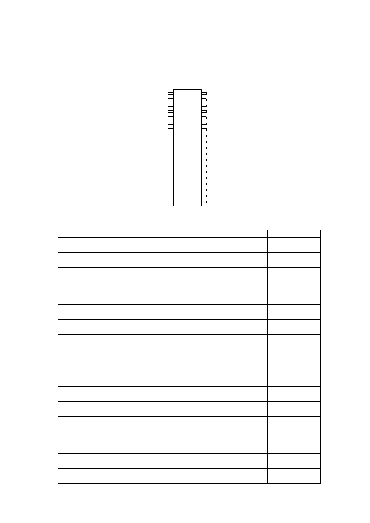
The interface between Main and Keypad PCBs is made via a 33-way connector.
INTERFACES AND TEST POINTS
10
11
12
13
14
15
16
17
18
19
1
7
9
VR
V[5]
V[4]
V[3]
V[2]
V[1]
CAP2+
CAP2-8
CAP1CAP1+
CAP3VOUT
GROUND
D2V8
DOUT
S_CLK
LCD_RS
nRESET
LCD_CS
10224-1
GROUND
BL4 2
VBAT 3
KBR(4) 4
KBR(3) 5
KBR(2) 6
KBR(1)
KBR(0)
KBC(4)
KBC(3)
KBC(2)
KBC(1)
KBC(0)
nPOWKEY
20
21
22
23
24
25
26
CN801
27
28
29
30
31
32
33
Figure 2.1: Interboard Connector
No. Signal Name MAIN <==> KEYPAD Function Connection
1 VR ==> LCD Voltage Reference
2 V[5] ==> LCD Voltage Reference
3 V[4] ==> LCD Voltage Reference
4 V[3] ==> LCD Voltage Reference
5 V[2] ==> LCD Voltage Reference
6 V[1] ==> LCD Voltage Reference
7 CAP2+ for LCD Stepup DC/DC
8 CAP2- for LCD Stepup DC/DC
9 CAP1- for LCD Stepup DC/DC
10 CAP1+ for LCD Stepup DC/DC
11 CAP3- for LCD Stepup DC/DC
12 VOUT
13 GND Ground GND
14 D28VB Power Source for LCD module D28VB
15 DOUT LCD control Serial data HERCULES pin 5
16 S_CLK LCD control Serial clock HERCULES pin 12
17 LCD_RS ==> LCD control Address data select HERCULES pin 59
18 nRESET ==> MPU nRESET signal
19 CS.LCD ==> LCD chip select signal HERCULES pin 14
20 GND Ground GND
21 BL[4] KEY Backlight ACC IC #49
22 VBAT Battery Voltage
23 KBR(4) <== Key Row 4 signal for Key scan HERCULES pin 179
24 KBR(3) <== Key Row 3 signal for Key scan HERCULES pin 178
25 KBR(2) <== Key Row 2 signal for Key scan HERCULES pin 176
26 KBR(1) <== Key Row 1 signal for Key scan HERCULES pin 174
27 KBR(0) <== Key Row 0 signal for Key scan HERCULES pin 173
28 KBC(4) ==> Key Column 4 signal for Key scan HERCULES pin 172
29 KBC(3) ==> Key Column 3 signal for Key scan HERCULES pin 171
30 KBC(2) ==> Key Column 2 signal for Key scan HERCULES pin 170
31 KBC(1) ==> Key Column 1 signal for Key scan HERCULES pin 169
32 KBC(0) ==> Key Column 0 signal for Key scan HERCULES pin 165
33 nPOWKEY <== Power Key sense signal OMEGA pin 74
MCUK001001G8 Section 2 Issue 1
Technical Guide – 3 – Revision 0
INTERFACES AND TEST POINTS
3
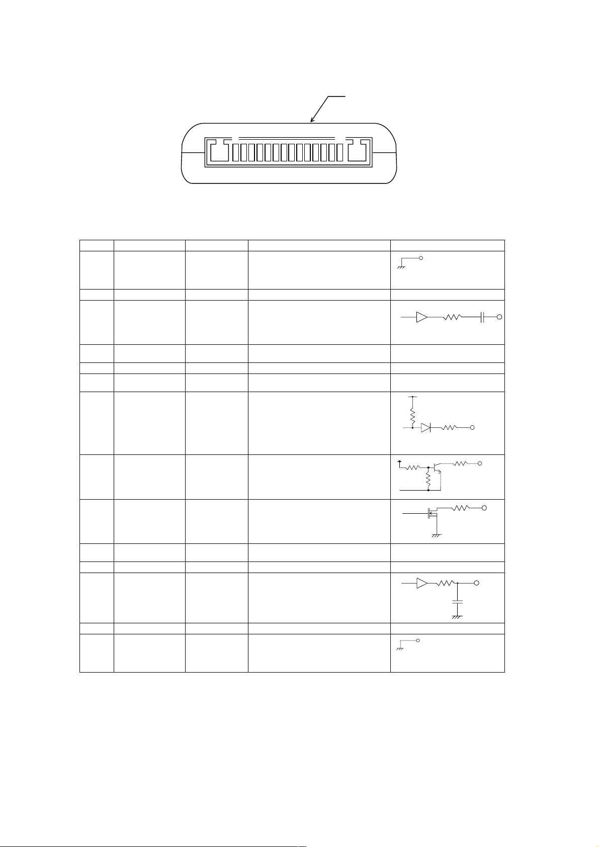
2.1.2 External I/O
No. Name HH <==>EXT Function H/H Circuit
1 AGND - Audio Ground
2 TX-AUDIO <== Sending Audio
3 RX-AUDIO ==> Received Audio
CASE FRONT
114
10225-1
Figure 2.2: External I/O Connector
10095-1
560
4 VBAT IN /
DATA_MODE0
<== Battery Voltage Supply input /
Data Accessory Recognition 0
5 nACC_SENSE <== Handsfree / Data Accessory detection
6 nAUDIO-ON ==> Audio Path Control
7 SERIAL UP <== Upward serial
8 SERIAL-DOWN ==> Downward serial
9 ACC_PWR ==> Peripheral power supply
10 DTR /
DATA_MODE1
<== RS232C: Data Terminal Ready /
(L: On = un mute, Hi-Z: Off = mute)
(9600 bps: SMS cable)
(33.8 kbps: Data adaptor I/F Card)
(up to 38.4 kbps: Soft Modem cable)
(57.6 kbps: Test Command)
(Baud rate same as SERIAL-UP)
(on: less than 100 mA)
Data Accessory recognition 1
11 RTS <== RS232C: Request to Send
12 CTS / PA-ON ==> PA control signal for test trigger
(L: off, H 2.8V: on)
13 EXT-PWR <== Power supply for Battery Charge
14 GND - Power supply and digital signal
ground
10222-1
4.7 k
10105-1
10097-1
10223-1
2.2k
0.1
330
330
47k
10104-1
330
30
330p
10095-1
Issue 1 Section 2 MCUK001001G8
Revision 0 – 4 – Technical Guide
2.1.3 SIM Interface
2.2. Test Points
2.2.1 Main PCB
INTERFACES AND TEST POINTS
Pin Signal
1SIMPWR (3V/5V)
2SIM_RST
3 SIM_CLK
4 Not connected
5 Ground
6 Not connected
7 SIM-I/O
8 Not connected
TP No. Signal
TP601 nAUDIO_ON
TP602 DTR/DATA_MODE1
TP603 RTS
TP604 CTS/PA_ON
TP605 SERIAL_DOWN
TP606 SERIAL_UP
TP607 VBAT_IN/DATA_MODE0
TP608 KBR[4]
TP609 KBR[3]
TP610 KBR[2]
TP611 KBR[1]
TP612 KBR[0]
TP613 KBC[4]
TP614 KBC[3]
TP615 KBC[2]
TP616 KBC[1]
TP617 KBC[0]
TP618 nPOWKEY
TP619 SIM I/O
TP620 SIMCLK
TP621 SIM RST
TP622 SIMPWR
TP623 HERCULES TX_IRDA
TP624 HERCULES RX_IRDA
TP625 HERCULES CLK32_OUT
TP626 A28V
TP627 D28VB
TP628 D28V
TP629 D18V
TP630 D20V
TP631 EARP
TP632 EARN
TP633 BAT_TEMP
TP634 BAT_ID
TP635 HF_TXAUDIO
TP636 HF_RXAUDIO
TP No. Signal
TP637 EXT_PWR
TP638 BL[1]
TP639 BL[2]
TP640 BL[3]
TP641 CHARGING_LED
TP642 PAGING_LED
TP643 VBAT
TP644 VBAT
TP645 U607 Pin 1 (32KOUT)
TP646 GROUND
TP647 GROUND
TP649 DTHFO_P
TP650 DTHFO_N
TP651 PHF_DET
TP652 HSRX_AUD
TP653 HSTX_AUD
TP654 E608 (MIC)
TP655 E607 (MIC)
TP656 n_ACC_SENSE
TP658 BL[4]
TP701 HERCULES TDI
TP702 HERCULES TDO
TP703 HERCULES TCK
TP704 HERCULES TMS
TP707 HERCULES nBSCAN
TP708 HERCULES SSDX
TP709 HERCULES SSDR
TP710 HERCULES SSCLK
TP711 HERCULES SSRST
TP712 OMEGA TESTRESET
TP713 OMEGA RESPWRONZ
TP715 OMEGA TDO
TP901 BACK_LED
MCUK001001G8 Section 2 Issue 1
Technical Guide – 5 – Revision 0

INTERFACES AND TEST POINTS
2.2.2 Keypad PCB
TP No. Signal
TP801 VBAT
TP802 DS801 / R801
TP803 DS802 / R801
TP804 DS803 / R802
TP805 DS804 / R802
TP806 DS805 / R803
TP807 DS806 / R803
TP808 DS807 / R804
TP809 DS808 / R804
TP810 nPOWKEY
TP811 KBR[0]
TP812 BL4
TP813 GROUND
Issue 1 Section 2 MCUK001001G8
Revision 0 – 6 – Technical Guide
RF OVERVIEW
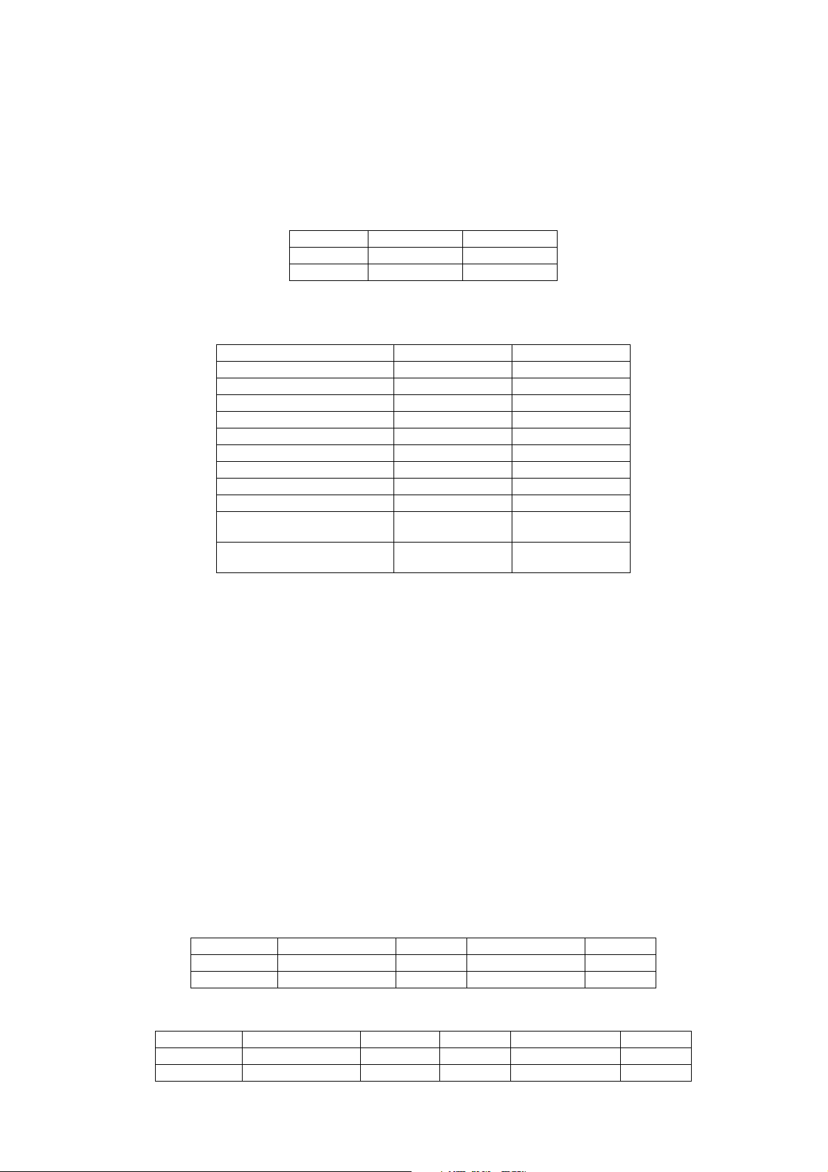
3 RF OVERVIEW
3.1. Introduction
3.1.1 General Specifications
The telephone is a Dual Band product incorporating two switchable transceivers, one for the GSM 900 band and another for
the GSM 1800 (DCS 1800) band. The transmit and receive bands for the mobile are given in the table below:
Tx Rx
GSM 900 890-915 MHz 935-960 MHz
GSM 1800 1710-1785 MHz 1805-1880 MHz
Other salient technical features are as follows:
GSM 900 GSM 1800
Rx Bandwidth 25 MHz 75 MHz
Tx Bandwidth 25 MHz 75 MHz
Duplex Spacing 45 MHz 95 MHz
Number of Channels 124 374
AFRCN (Channel Numbers) 1-124 512-885
1st Tx Channel 890.2 MHz 1710.2 MHz
Last Tx Channel 914.8 MHz 1784.8 MHz
1st Rx Channel 935.2 MHz 1805.2 MHz
Last Rx Channel 959.8 MHz 1879.8 MHz
Maximum Tx Power 33.0 dBm
(Class 4) (PL5)
Minimum Tx Power 5.0 dBm
(PL19)
30.0 dBm
(Class 1) (PL0)
0.0
(PL15)
3.1.2. Main PCB Description
All components required for the RF and Logic circuits, excluding the LCD module and backlight LEDs, are contained on the
Main PCB. The Main PCB has six layers with an Any Layer Interstitial Via-Hole (ALIVH) structure which can connect from / to
any layer. Surface and back layer tracks are gold-plated to prevent oxidisation and enable better soldering. The PCB thickness
is 0.7 mm ±0.1 mm.
The majority of RF components are located on both sides of the top half area of the Main PCB. The Keypad PCB back layer
consists mostly of groundplane which is used to provide RF shielding. A metallised plastic chassis has also been designed to
provide smaller walled sections to isolate sensitive RF areas like the synthesiser block from high level interference such as the
PA output and logic noise.
The back cover has a formed shielded enclosure to reduce further spurious emissions and logic noise.
3.2. Functional Description
3.2.1. Frequency Plan
The frequency plan is shown below:
Tx Tx IF RFLO Tx IFLO Tx
GSM 900 890 - 915 MHz 270 MHz 1160 - 1185 MHz 540 MHz
GSM 1800 1710 - 1785 MHz 135 MHz 1575 - 1650 MHz 540 MHz
Rx Rx 1st IF Rx 2nd IF RFLO Rx IFLO Rx
GSM 900 935 - 960 MHz 225 MHz 45 MHz 1160 - 1185 MHz 540 MHz
GSM 1800 1805 - 1880 MHz 225 MHz 45 MHz 1580 - 1655 MHz 540 MHz
MCUK001001G8 Section 3 Issue 1
Technical Guide – 7 – Revision 0
RF OVERVIEW
RF Switch
935 ~ 960 MHz
1,805 ~
1,880 MHz
Dual Rx
SAW BPF
RF VCO
1,160 ~ 1,185 MHz
1,575 ~ 1,655 MHz
Coupler
w/ LPF
Coupler
w/ LPF
LC BPF
GSM: 1,160 ~ 1,185 MHz
DCS: Rx 1,580 ~ 1,655 MHz
Tx 1,575 ~ 1,650 MHz
RF
Synthe
APC
IC
Dual PA
PF08103B-02- TB
(Hitachi)
Bright III RF IC
HD155133TFEB
IF VCO
(VJ3)
Tx VCO
890 ~ 915 MHz
1,710 ~ 1,785 MHz
IF SAW
BPF
225 MHz
2 2
Synthe
IF
%2
Phase
Detector
270 MHz
DCS: 270 MHz
GSM: 540 MHz
GSM: 270 MHz
DCS: 134, 135 MHz
45 MHz
%6
TCXO
(NDK)
%2
I&Q
Mod
%2
GSM: 270 MHz
DCS: 135 MHz
10213-1
935-960 MHz
RF LO
1160-1185 MHz
Figure 3.1: RF Block Diagram
Rx 1st IF
225 MHz
270 MHz
Fdiff
270 MHz
TX VCO
890-915 MHz
Rx 2nd IF
45 MHz
÷2
Fcomparison
270 MHz
Figure 3.2: GSM 900 Frequency Plan
45 MHz
÷2
÷2
270 MHz
I
Q
90 MHz
÷6
IF LO
VCO
540 MHz
I
Q
10214-1
Issue 1 Section 3 MCUK001001G8
Revision 0 – 8 – Technical Guide
RF OVERVIEW
1805-1880 MHz
Rx RF LO
1580-1655 MHz
Tx RF LO
1575-1650 MHz
Rx 1st IF
225 MHz
270 MHz
Fdiff
135 MHz
TX VCO
1710-1785 MHz
Rx 2nd IF
45 MHz
Fcomparison
135 MHz
45 MHz
÷2
270 MHz
÷2
÷2
I
Q
90 MHz
÷6
IF LO VCO
540 MHz
135 MHz
I
Q
10215-1
Figure 3.3: GSM 1800 Frequency Plan
3.2.2 General
The RF circuit design is built around an Hitachi Bright III GSM transceiver IC. Other major components include filters, power
amplifiers, VCOs and the antenna subsystems.
In either band, GSM 900 or GSM 1800, the Rx IF is fixed at 225 MHz and the 2nd IF at 45 MHz. Therefore, the 2nd local
oscillator is fixed at 540 MHz for receiver modes. This oscillator is also fixed at 540 MHz for transmit modes.
The Tx VCO is on-channel in both GSM 900 and GSM 1800 modes of operation.
3.2.3 Antenna
The antenna is a fixed helical type.
A mechanical switch is used to route the RF signal from the external antenna for handsfree operation and test purposes.
3.2.4 Transmit and Receive
The transmit and receive paths are covered in their own specific chapters later in this manual.
3.2.5 RF and Accessory Connector
An external antenna connector for use with handsfree accessories is located close to the PA module to minimise power loss.
Therefore, the PAs do not have to be driven so hard, allowing the voltage supply to be lower, thus improving battery
performance.
MCUK001001G8 Section 3 Issue 1
Technical Guide – 9 – Revision 0

RF OVERVIEW
This page is intentionally blank.
Issue 1 Section 3 MCUK001001G8
Revision 0 – 10 – Technical Guide
 Loading...