Panasonic GD90 Service Manual
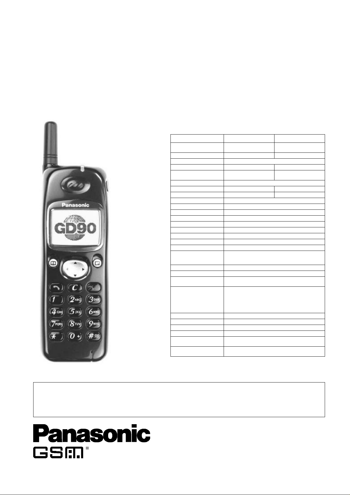
Order Number: MCUK990801G8
Technical Guide
GD90 Personal Cellular Telephone
Handheld Portable
Specification
900MHz 1800MHz
Frequency range Tx: 890 - 915 MHz
Tx/Rx frequency separation 45 MHz 95 MHz
RF channel bandwidth 200 kHz
Number of RF channels 124 374
Speech coding Full rate/Half rate/Enhanced
Operating temperature -10°C to +55°C
Type Class 4 Handheld Class 1 Handheld
RF Output Power 2 W maximum 1W maximum
Modulation GMSK (BT = 0.3)
Connection 8 ch/TDMA
Voice digitizing 13 kbps RPE-LTP / 13 kps ACLEP / 5.6 kps CELP / VSLEP
Transmission speed 270.3 kbps
Diversity Frequency hopping
Signal Reception Double superheterodyne
Intermediate Frequency 282MHz and 45MHz
Antenna Terminal Impedance 50 Ω
Antenna VSWR <2.1 : 1
Dimensions Height: 118 mm
Volume 84.5 cc
Weight 88 g
Display Graphical chip on glass liquid crystal, Alphanumeric 16 x 3
Illumination Green:
Keypad 17 keys, Navigation key
SIM Plug-in type only
External DC Supply Voltage 3.6V
Battery 3.6V
Standby Battery Life
DRX 9
Conversation Battery Life
PL 7, DTX 50%
Rx: 935 - 960 MHz
Full rate
Width: 42 mm
Depth: 16.5 mm
characters, 5 icons and 6 x 1 characters
4 LEDs for the LCD
8 LEDs for the keyboards
1 LED Incoming call
Red:
1 LED Charging indicator
95 hrs maximum
200minutes
Tx: 1710 - 1785 MHz
Rx: 1805 - 1880 MHz
Full rate/Half rate
EB-GD90
Unless stated these specifications are with Battery Pack (EB-BSD90) fitted.
Battery life figures are dependent on network conditions.
WARNING
This service information is designed for experienced repair technicians only and is not designed for use by the general public. It does not contain warnings or
cautions to advise non-technical individuals of potential dangers in attempting to service a product.
Products powered by electricity should be serviced or repaired only by experienced professional technicians. Any attempt to service or repair the product or
products dealt with in this service manual by anyone else could result in serious injury or death.
Issue 1
Revision 0

This Technical Guide is copyright and issued on the strict understanding that it is not to be reproduced, copied, or disclosed to
any third party, either in whole or part, without the prior written consent of Matsushita Communication Industrial UK Ltd.
Every care has been taken to ensure that the contents of this publication give an accurate representation of the equipment.
However, Matsushita Communication Industrial UK Ltd. accepts no responsibility for inaccuracies which may occur and
reserves the right to make changes to the specification or design without prior notice.
The information contained in this manual and all rights in any designs disclosed therein, are and remain the exclusive property
of Matsushita Communication Industrial UK Ltd.
Other patents applying to material contained in this publication:
BULL CP8 PATENTS
Comments or correspondence concerning this manual should be addressed to:
Customer Support Department,
Matsushita Communication Industrial UK Ltd.,
Colthrop,Thatcham,
Berkshire. RG19 4ZD.
ENGLAND
© 1999 Matsushita Communication Industrial UK Ltd.
Issue 1 – ii – MCUK990801G8
Revision 0 Technical Guide

CONTENTS
1 INTRODUCTION
1.1 Purpose of this Guide . . . . . . . . . . . . . . . . . . . . . . . . . . . 1
1.2 Structure of the Guide . . . . . . . . . . . . . . . . . . . . . . . . . . . 1
2 INTERFACES AND TEST POINTS
2.1 Interfaces . . . . . . . . . . . . . . . . . . . . . . . . . . . . . . . . . . . . 3
3 RF OVERVIEW
3.1 Introduction . . . . . . . . . . . . . . . . . . . . . . . . . . . . . . . . . . .7
3.2 Functional Description . . . . . . . . . . . . . . . . . . . . . . . . . . 7
3.3 RF & Accessory Connector . . . . . . . . . . . . . . . . . . . . . . 10
4 TRANSMITTER
4.1 Introduction . . . . . . . . . . . . . . . . . . . . . . . . . . . . . . . . . .11
4.2 Functional Description . . . . . . . . . . . . . . . . . . . . . . . . . 12
5 RECEIVER
5.1 Introduction . . . . . . . . . . . . . . . . . . . . . . . . . . . . . . . . . .15
5.2 Functional Description . . . . . . . . . . . . . . . . . . . . . . . . . 16
6 BASEBAND OVERVIEW
6.1 Introduction . . . . . . . . . . . . . . . . . . . . . . . . . . . . . . . . . .19
6.2 Functional Description of the PCB . . . . . . . . . . . . . . . . 19
7 GEMINI
7.1 Introduction . . . . . . . . . . . . . . . . . . . . . . . . . . . . . . . . . .25
7.2 Functional Description . . . . . . . . . . . . . . . . . . . . . . . . . 25
8 VEGA
8.1 Introduction . . . . . . . . . . . . . . . . . . . . . . . . . . . . . . . . . .29
8.2 Functional Description . . . . . . . . . . . . . . . . . . . . . . . . . 29
9 POWER SUPPLIES
9.1 Introduction . . . . . . . . . . . . . . . . . . . . . . . . . . . . . . . . . .33
9.2 Overview . . . . . . . . . . . . . . . . . . . . . . . . . . . . . . . . . . . . 33
9.3 Power-up . . . . . . . . . . . . . . . . . . . . . . . . . . . . . . . . . . . . 33
9.4 Power-down . . . . . . . . . . . . . . . . . . . . . . . . . . . . . . . . . 34
9.5 Power Management . . . . . . . . . . . . . . . . . . . . . . . . . . . 35
MCUK990801G8 Section Issue 1
Technical Guide – iii – Revision 0

This page is left intentionally blank.
Issue 1 Section MCUK990801G8
Revision 0 – iv – Technical Guide

INTRODUCTION
1 INTRODUCTION
1.1 Purpose of this Guide
This guide contains technical information for the Panasonic GD90 personal cellular telephone system operating on the GSM
network. Procedures for installing, operating and servicing (e.g. disassembly and testing) the telephone system are provided
in the associated Service Manual.
1.2 Structure of the Guide
The guide is structured to provide service-engineering personnel with the following technical information on the GSM mobile
telephone:
1. Interface details and relevant test points.
2. Functional description of each section of the mobile telephone.
3. Detailed description of each section of the mobile telephone.
MCUK990801G8 Section 1 Issue 1
Technical Guide – 1 – Revision 0

INTRODUCTION
This page is left intentionally blank.
Issue 1 Section 1 MCUK990801G8
Revision 0 – 2 – Technical Guide
INTERFACES AND TEST POINTS
2 INTERFACES AND TEST POINTS
2.1 Interfaces
2.1.1 Main and Keypad PCBs
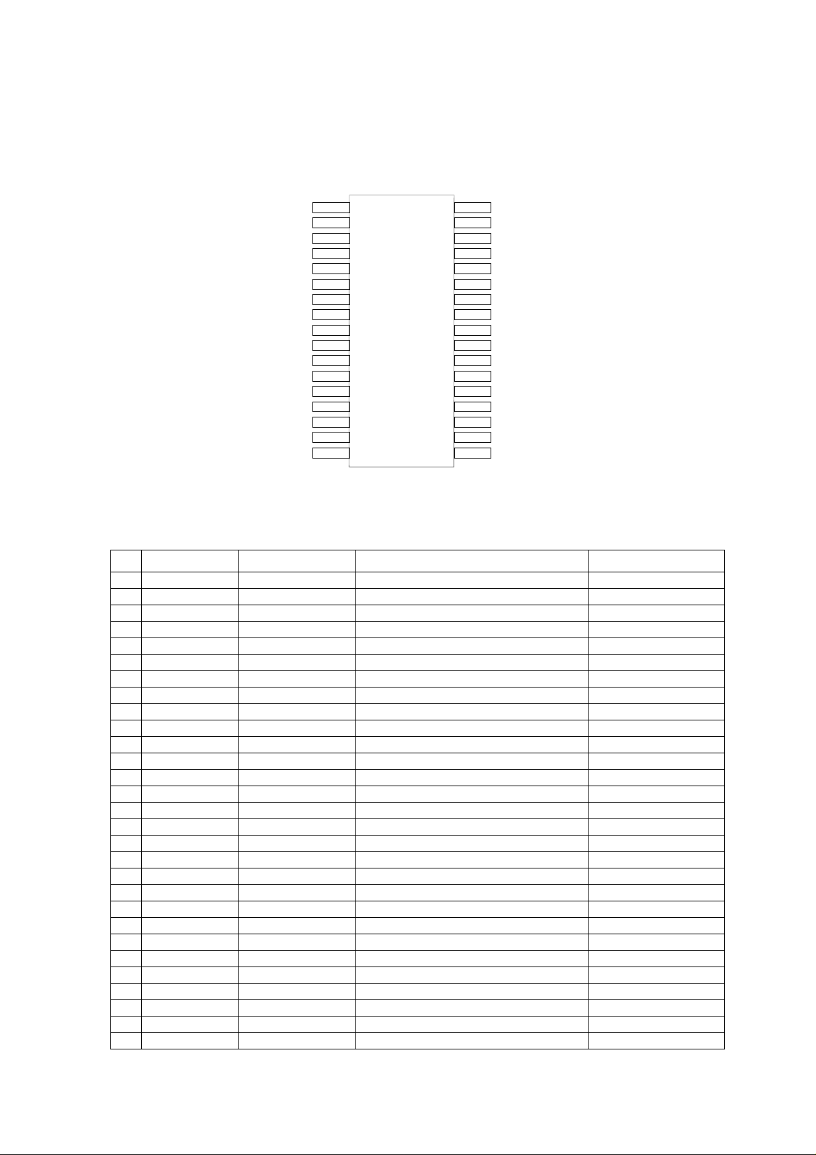
The interface between Main and Keypad PCBs is made via a 34-way connector as follows:
GND
D28V
KEYBKLT
LCD_GRN
LCD_RED
A(1)
RnV
KBC(4)
KBC(3)
KBC(2)
KBC(0)
KBC(1)
D(4)
D(3)
D(2)
D(1)
D(0)
1
2
3
4
5
6
7
8
9
10
11
12
13
14
15
16
17
18
19
20
21
22
23
24
25
26
27
28
29
30
31
32
33
34
GND
D28V
nPOWKEY
PAGING_LED
CHARGING_LED
nRESET
CS_LCD
KBR(3)
KBR(2)
KBR(4)
KBR(1)
KBR(0)
D(5)
D(6)
D(7)
REC_P
REC_N
10075-1
Figure 2.1: GD90 Interboard Connector
No. Signal Name MAIN <=> KEYPAD Function Connection
1 GROUND 2 D28V - Power Source for LCD Module
3 K EY BK LT ==> Key Backlight Power Source Charge IC pin 16
4 LCD_GRN ==> LCD Green Backlight Power Charge IC pin 18
5 LCD_RED ==> LCD Red Backlight Power Charge IC pin 17
6 A(1) ==> MPU Address bus (1) GEMINI pin 25
7 RnW ==> MPU Read/nWrite signal GEMINI pin 20
8 K BC( 4) ==> Key Column 4 signal for Key scan GEMINI pin 128
9 K BC( 3) ==> Key Column 3 signal for Key scan GEMINI pin 129
10 KBC(2) ==> Key Column 2 signal for Key scan GEMINI pin 130
11 KBC(0) ==> Key Column 0 signal for Key scan GEMINI pin 132
12 KBC(1) ==> Key Column 1signal for Key scan GEMINI pin 133
13 D(4) <==> MPU Data bus (4)
14 D(3) <==> MPU Data bus (3)
15 D(2) <==> MPU Data bus (2)
16 D(1) <==> MPU Data bus (1)
17 D(0) <==> MPU Data bus (0)
18 GROUND - l
19 D28V - Power Source for LCD Module
20 nPOWKEY <== Power Key sense signal
21 PAGING_LED ==> Paging LED control signal SIM_PWR IC pin 22
22 CHARGE_LED ==> Charge LED control signal GEMINI pin 105
23 nRESET ==> MPU nRESET signal
24 CS_LCD ==> LCD chip select signal GEMINI pin 55
25 KBR(3) <== Key Row 3 signal for Key scan GEMINI pin 123
26 KBR(2) <== Key Row 2 signal for Key scan GEMINI pin 124
27 KBR(4) <== Key Row 4 signal for Key scan GEMINI pin 122
28 KBR(1) <== Key Row 1 signal for Key scan GEMINI pin 125
29 KBR(0) <== Key Row 0 signal for Key scan GEMINI pin 126
MCUK990801G8 Section 2 Issue A
Technical Guide – 9 – Revision 0
INTERFACES AND TEST POINTS
k
k
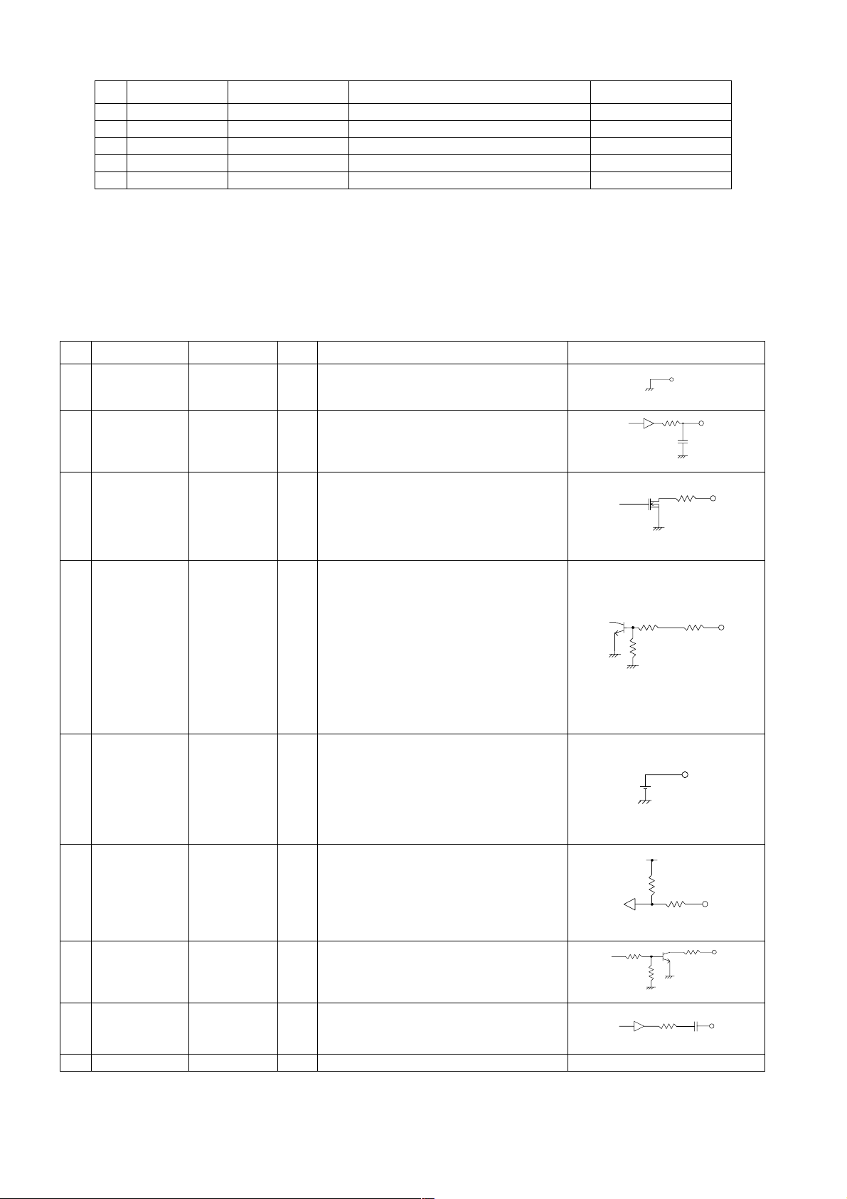
No. Signal Name MAIN <=> KEYPAD Function Connection
30 D(5) <==> MPU Data bus (5)
31 D(6) <==> MPU Data bus (6)
32 D(7) <==> MPU Data bus (7)
33 REC_P ==> R eceiver Pos itive Output
34 REC_N ==> Receiver Negative Output
GD90 has two external connectors:
1. a multi-way connector for use with a handsfree data;
2. additional contacts for charging the battery pack while in the desktop charger;
All interfaces are electrically and mechanically compatible with GD90.
Main Unit <==> External I/O
No. Name H/H <=> EXT Total Function H/H Circuit
1 GND ==> 6 Ground
10095-1
2 PA_ON ==> 1 Gating of spectrum analyser for Transmitter
performance testing
L: Off, Hi - Z: On)
3 nLOGIC_PWR ==> 1 Accessory Power Control signal.
In the handsfree this is logical OR’ed with
IGNITION in order that the software can
maintain the Handsfree power-on state if the
user is in a call and that the IGNITION is
switched off. L: Power-on, Hi-Z: Power-off
4 IGNITION <== 1 IGNITION is used in two cases.
1) Determine the mode of operation of the H/H
when the Handsfree accessory is attached.
L: At a suitable time enter dummy sleep mode
and therefore minimise the drain on the car
battery (nLOGIC_POWER = Hi - Z)
H: Normal mode
2) Satisfy 2nd of 2 conditions for sending
initialise T est set command and entering Testset
mode. (see nADP_SENSE for 1st condition)
L: Condition 2 satisfied
H: Enter Testset mode not satisfied
5 VBAT <=> 1 The pin is either an input or an output
depending upon the battery connection.
1) Battery/Dummy battery connected: Output
supply terminal for attached accessories.
2) No connection: Low current input supply
terminal for non-RF performance checking in
Testset Mode or Flash programming.
10097-1
10096-1
10k
330p
330
50k
200
330
10098-1
10099-1
6 nH/F_SENSE <== 1 Handsfree sense line
L: connected
H (internal pull-up): disconnected
7 nRADIO_MUTE ==> 1 Radio Mute
L: mute, Hi-Z: unmute)
8 RX_AUDIO ==> 1 Accessory Receiving Audio
-16 dBm0 = 76.7m Vrms
10100-1
10102-1
100k
330
50k
200
330
10101-1
560
1F
9 GND ==> Ground Refer to pin 1
Issue A Section 2 MCUK990801G8
Revision 0 – 10 – Technical Guide
INTERFACES AND TEST POINTS
k
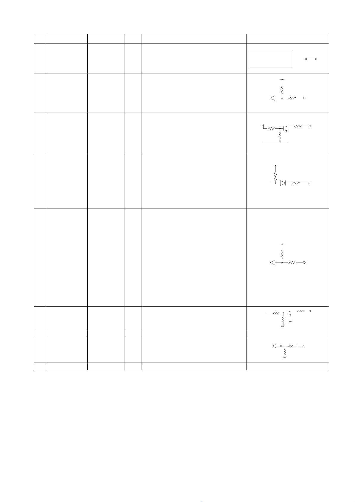
No. Name H/H <=> EXT Total Function H/H Circuit
10 EXT-PWR <== 2 Power supply for battery charging, Power ON/
Off control and accessory control circuits.
Voltage: 5.8 ± 0.2 V
Current: 650 ± 50 mA
Trickle Charge Circuit
Power On/Off Control Circuit
Rapid Charge Circuit
Accessory Control Circuit
10103-1
11 NON_HOOK <== 1 Indicates if the optional second handset is on or
off hook. In handsfree operation, if the optional
handset is not fitted this signal defaults to on
hook. (Low.)
10100-1
12 SERIAL_OUT ==> 1 Downlink Serial Data
(Baud rate is same as SERIAL_IN)
2.2k
13 SERIAL_IN <== 1 Uplink Serial Data
The baud rate is dependant upon the attached
accessory, whether operating in Testset Mode
or Flash Downloading.
SMS cable: 9600 bps
RS232 Direct cable: 38.4 kbps
4.7 k
10105-1
Data adapter: 33.8 kbps
Testset: 9600 bps
Flash Download: 56 kbps
14 nADP_SENSE <== 1 NADP_SENSE has 5 possible states. The state
is determined by the value of the pull-down
resistor in the attached accessory / test set.
NADP_SENSE has 2 purposes as follows:
1) To identify an attached accessory.
Open (H): No attached accessory
82 kΩ=± 1% (MH): Headset Adapter
56 kΩ=± 1% (M): SMS Cable
33 kΩ=± 1% (ML): RS232C Direct Cable
GND (L): Data Adapter
2) Determine whether the 1st of 2 conditions
10100-1
are satisfied for sending the initialise Testset
command on SERIAL_OUT, and entering
Testset mode (see IGNITION for 2nd condition).
H/MH: Condition 1 satisfied
M/ML/L: Enter Testset Mode not satisfied
15 NH/F_ON ==> 1 Accesso ry Sending & Receiving Audio paths
unmute
L: unmute, Hi-Z: mute
16 GND ==> 6 Refer to pin 1 Refer to pin 1
17 TX_AUDIO <== 1 Accessory Sending Audio
-16 dBm0 = 40.4 m Vrms
18 GND ==> 6 Ground connection of Dual Charger Refer to pin 1
100k
330
100k
330
10104-1
330
330
330
10101-1
11
10k
3k3
10106-1
47k
50k
200
MCUK990801G8 Section 2 Issue A
Technical Guide – 11 – Revision 0
INTERFACES AND TEST POINTS
No. Name H/H <=> EXT Total Function H/H Circuit
19 GND ==> 6 Ground connection of Dual Charger Refer to pin 1
20 GND ==> 6 Ground connection of Dual Charger Refer to pin 1
21 GND ==> 6 Ground connection of Dual Charger Refer to pin 1
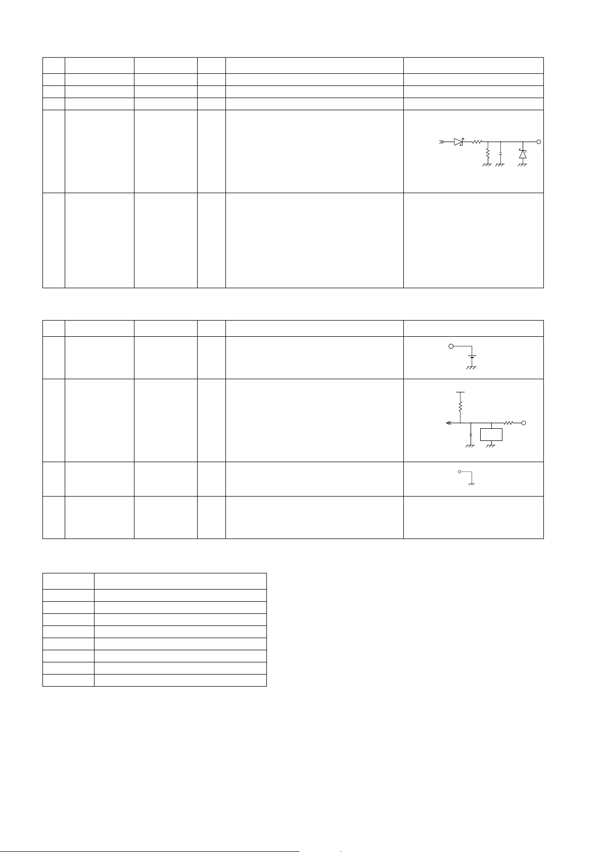
22 CHARGE_ON <=> 1 The Dual Charger shall hold CHARGE_ON to
the middle level unit a H/H is inserted into the
front slot.
H: 2.0<=V<=3.0 volts; Dual Charger detects
CHARGE_ON
connection of H/H
M: 1.0<=V<2.0 volts; Unconnected
10107-1
L: 0.0<=V<1.0 volts; Dual Charger detects
connection of H/H
23 EXT_PWR <== 2 The Dual Charger shall control switching of the
Refer to pin 8
power supply to the front slot (corresponds to
EXT_PWR) based on the state of the
CHARGE_ON signal.
H: EXT_PWR supplied
L: When the H/H can determine whether or not
to set CHARGE_ON. After the in ser tion of the
H/H, EXT_PWR shall be subsequently supplied
TBA hours
within
Battery Connector
330
10k
0.1µ
No. Name H/H <=> EXT Total Function H/H Circuit
1 VBAT <== 1 Positive battery terminal.
Li+ (2 cells in parallel): 3.6 V nom.
NiMH (3 cells in series): 3.6 V nom.
2 BAT_TEMP <== 1 BAT_TEMP has 2 purposes.
1) Determine whether a battery is attached to
the H/H.
2) Monitor battery temperature for the purposes
of charging.
Vega_ADIN2
H: Abnormal battery
M: Li+ or NiMH charging
L: No battery or abnormal battery
3 GND <== 1 Negative battery terminal
4 BAT_ID <== 1 BAT_ID is used to identify the type of attached
battery.
H: Li+ or no battery
L: NiMH
SIM Interface
Pin Signal
1GND
25 V
3 Not connected
4 Reset
5 Serial input/output
6 Clock
7 Not connected
8 Not connected
ChargerIC VREFOUT
10108-1
Protection
10110-1
ESD
ESD
10109-1
Issue A Section 2 MCUK990801G8
Revision 0 – 12 – Technical Guide

RF OVERVIEW
3 RF OVERVIEW
3.1 Introduction
3.1.1 General Specifications
GD90 is a Dual Band product incorporating two switchable transceivers, one for the GSM900 band and another for the
GSM1800 (DCS1800) band. The transmit and receive bands for the mobile are given in the table below:
Tx Rx
GSM900 890-915MHz 935-960MHz
GSM1800 1710-1785MHz 1805-1880MHz
Other salient technical features are as follows:
GSM900 GSM1800 Units
Rx Bandwidth 25 75 MHz
Tx Bandwidth 25 75 MHz
Duplex Spacing 45 95 MHz
Number of Channels 124 374
ARFCN (Channel Numbers) 1-124 512-885
1st Tx Channel 890.2 1710.2 MHz
Last Tx Channel 914.8 1784.8 MHz
1st Rx Channel 935.2 1805.2 MHz
Last Rx Channel 959.8 1879.8 MHz
Maximum Tx Power 33.0
(Class 4) (PL5)
Minimum Tx Power 5.0
(PL19)
30.0
(Class 1) (PL0)
0.0
(PL15)
dBm
dBm
3.1.2 Description of Main PCB
All components required for the RF and Logic circuits, excluding the LCD module and backlight LEDs, are contained on the
Main PCB. The Main PCB has six layers made from FR4 material (Epoxide woven glass fabric copper-clad laminate as
specified in BS4584 Part 102 and prepeg as specified in BS4584 Part 103). Top and bottom layer tracks are gold-plated to
prevent oxidisation and enable better soldering. The board thickness is 0.9 mm (±0.1 mm).
The RF components are located on both sides of the upper area of the Main PCB. To provide RF shielding, most of one side
of the Keypad PCB comprises a printed circuit groundplane. The Main board is connected to the Keypad PCB via a 34-way
dual in-line connector. A metallised plastic chassis is used to separate the Main and the Keypad PCB’s. When the chassis is
sandwiched between the Main and the Keypad PCB’s, the groundplane of the Main board together with the chassis forms an
effective shielded enclosure which prevents spurious emissions. The chassis has also been designed to provide smaller walled
sections which are used to isolate sensitive RF areas such as the VCTCXO and the VCO from high level interferers such as
the PA output.
3.2 Functional Description
3.2.1 Frequency Plan
The GD90 frequency plan is shown below
Tx Tx IF RFLO Tx IFLO Tx Unit
GSM900 890-915 270 1160-1185 540 MHz
GSM1800 1710-1785 130 1580-1655 520 MHz
.
Rx Rx 1st IF Rx 2nd IF RFLO Rx IFLO Rx Unit
GSM900 935-960 225 45 1160-1185 540 MHz
GSM1800 1805-1880 225 45 1580-1655 540 MHz
MCUK990801G8 Section 3 Issue 1
Technical Guide – 7 – Revision 0
Issue A Section 3 MCUK990801G8
Revision 0 – 14 – Technical Guide
RF OVERVIEW
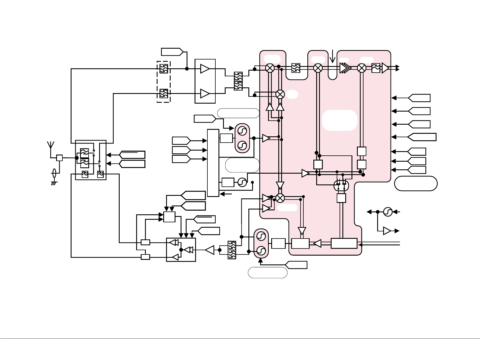
Figure 3.1: RF Block Diagram
ANT
Diplexer + 2
SW
LMC36-07A0503A
(MURATA)
DUAL RX SAW
V_PAON
V_PAON
DUAL APC IC
HD155171T
3.8*3.8mm
(MACO)
(HITACHI)
LDC15H200J0897
PCNnGSM
LPF Coupler
(DCS)
(MURATA)
CLOCK
DATA
STROBE
PLL IC
MB15F03SL
[SSOP Package]
(Fujitsu)
PCNnGSM
RAMP DATA
DUAL LNA IC
GN01073B
(MEC)
DCS
LNA
GSM
LNA
PCNnGSM
PLL
IC
2nd LOCAL VCO
PCNnGSM
PCNnGSM
DUAL RX SAW
Filter 3.8*3.8mm
(MACO)
(DCS)
(GSM)
DUAL LOCAL VCO
UY76043A
(MACO)
GSM:1160~1185MHz
DCS:1580~1655MHz
LOOP
FILTER
GSM:540MHz
DCS TX:520MHz
RX:540MHz
LOOP
FILTER
13MHz
(MACO)
DCS
Mixer
FILTER
EFCH225MDQP2
DC
MIXER
LOOP
(MACO)
IF SAW
(225MHz)
GSM
Mixer
PHASE
DETECTOR
2nd
Mixer
1/2
45MHz
HITACHI
BRIGHT-2
HD155123F
MODULATOR
1/2
PGC
I&Q
Demod
1/2
1/6
To
PLL IC
13MHz VCXO
7.0*5.0mm
(NDK)
I
Q
TXON1
RXON1
RXON2
PCNnGSM
CLOCK
DATA
STROBE
3 wire bus control
1st, 2nd Mixer Gain
PGC Gain
AFC
Ref.
Clock
I
Q
LPF Coupler
(GSM)
LDC15H200J0897
(MURATA)
Dual PA
PF08103B
(HITACHI)
Exciter
MGA-81563
(HP)
DUAL TX SAW
Filter
3.8*3.8mm
(MACO)
GSM:890~915MHz
DCS:1710~1785MHz
TX DUAL VCO
UY76044
PCNnGSM
10076-1
RF OVERVIEW
935-960MHz
RF LO
1160-1185MHz
1805-1880MHz
Rx 1st IF
225MHz
270MHz
Fdiff
270MHz
TX VCO
890-915MHz
Rx 2nd IF
45MHz
÷2
Fcomparison
270MHz
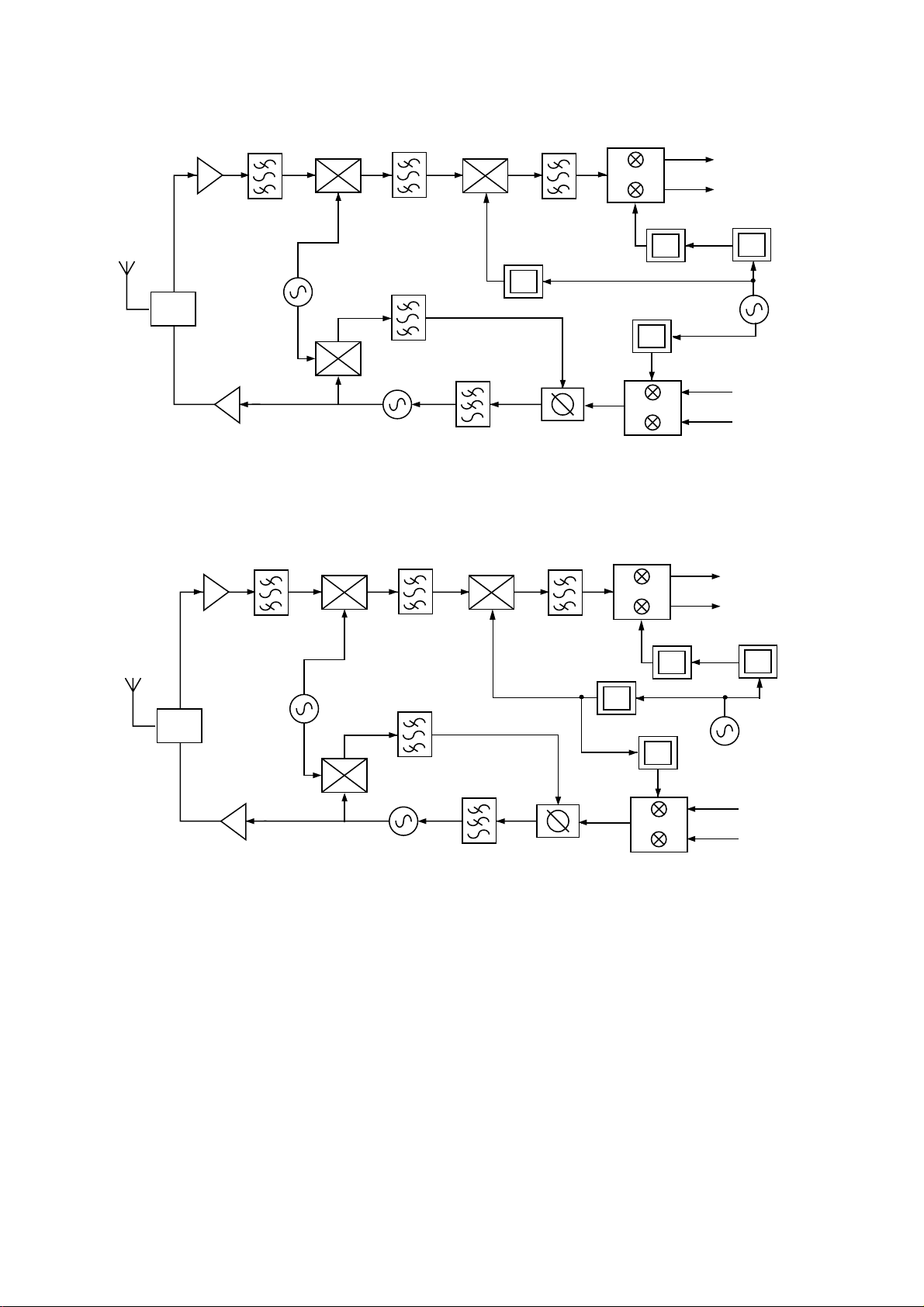
Figure 3.2: GSM 900 Frequency Plan
Rx 1st IF
225MHz
Rx 2nd IF
45MHz
45MHz
÷2
÷2
I
Q
90MHz
÷6
IF LO
VCO
540MHz
270MHz
I
Q
10077-1
I
Q
÷2
÷2
90MHz
÷6
IF LO VCO
Rx: 540MHz
Tx: 520MHz
I
Q
10078-1
RF LO
1580-1655MHz
Fdiff
130MHz
TX VCO
1710-1785MHz
270MHz
45MHz
÷2
260MHz
Fcomparison
130MHz
Figure 3.3: GSM 1800 Frequency Plan
3.2.2 General
The major building blocks for the RF design are the Hitachi transmit (Tx) and receive (Rx) IC, Fujitsu RF-IF dual PLL and the
antenna subsystem.
In either receiver band, GSM900 or GSM1800, the Rx 1st IF is fixed at 225 MHz and 2nd IF at 45MHz. Therefore, the 2nd
local oscillator is fixed at 540 MHz for receive mode.
In GSM900 transmit mode, the 2nd LO is reprogrammed to 540 MHz, the same for receive mode.
In GSM1800 mode, the 2nd loc al oscill ator is re-pro grammed to 52 0 MHz. For this choice o f IF, no tran smitter in-b and spuriou s
is believed to occur due to harmonics of the 1st LO.
The Tx VCO will be on-channel in either GSM900 or GSM1800 modes of operation.
MCUK990801G8 Section 3 Issue A
Technical Guide – 15 – Revision 0

RF OVERVIEW
3.2.3 Antenna
The antenna is a fixed helical type.
A mechanical RF switch is used to route the RF signal from the external antenna for handsfree operation and test purposes.
3.2.4 Transmit and Receive
The transmit and receive paths of GD90 are covered in their own specific chapters later in this manual.
3.3 RF & Accessory Connector
In previous models the RF signal is routed to the accessory connector which contains a micro-switch. If the switch is open, the
RF signal is routed to the hands free unit. If it closed, the signal is routed back via the Main PCB to the antenna. This routing
of the RF signal up and down the Main PCB invariably has a finite power loss associated with it.
In addition, the GD90 has a limited PCB area and the routing of the RF signal in this way reduces further the available PCB
area required for the Dual Band circuit.
To alleviate these problems the RF connector is located close to the PA module. This reduces the loss and hence the PAs do
not have to be driven so hard. This allows the power supply voltage to be lower, thus improving battery performance.
Issue 1 Section 3 MCUK990801G8
Revision 0 – 10 – Technical Guide
 Loading...