

Page 1
ORDER NO. KM40510896CE
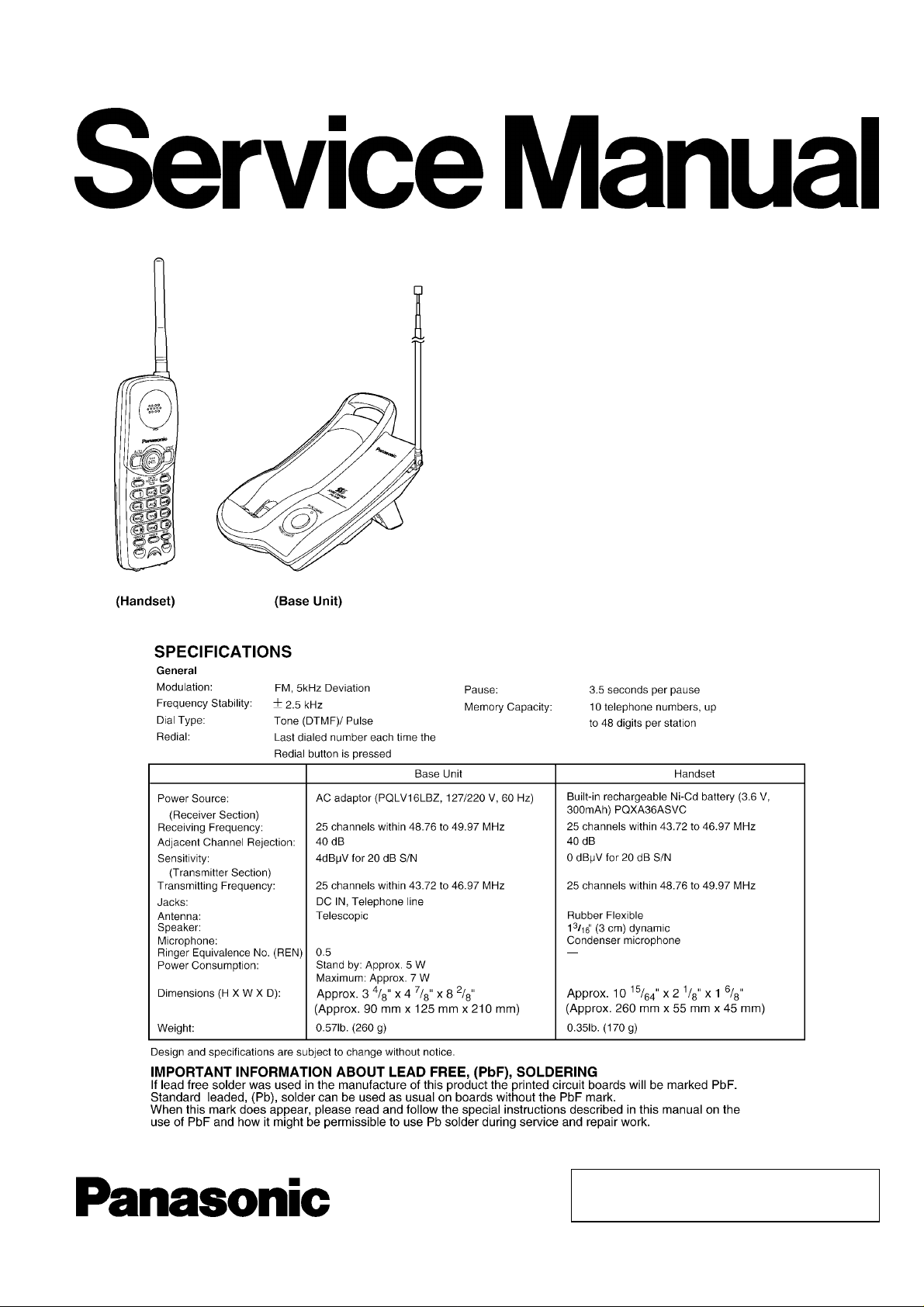
Telephone Equipment
KX-TC2105LBB
Cordless Phone
Black Version
(for Brazil)
© 2005 Panasonic Communications Co., Ltd. All
rights reserved. Unauthorized copying and
distribution is a violation of law.
Page 2
KX-TC2105LBB
Note:
Because CONTENTS 4 is the extract from the Operating Instructions of this model, it is subject to change without notice. You can
download and refer to the original Operating Instructions on TSN Server for further information.
CONTENTS
Page Page
1 ABOUT LEAD FREE SOLDER (PbF: Pb free) 4
1.1. Suggested PbF Solder
1.2. How to recognize that Pb Free Solder is Used
2 FOR SERVICE TECHNICIANS
3 CAUTION
4 OPERATING INSTRUCTIONS
4.1. Battery
4.2. Location of Controls
4.3. Connection
4.4. Troubleshooting
5 DISASSEMBLY INSTRUCTIONS
6 TROUBLESHOOTING GUIDE
6.1. Check Power
6.2. Bell Reception
6.3. Check Battery Charge
6.4. Check Link
6.5. Check Handset Transmission
6.6. Check Handset Reception
7 ADJUSTMENTS (BASE UNIT)
7.1. Test Mode Flow Chart (Base Unit)
7.2. How to change the channel
7.3. Adjustment
7.4. Adjustment Standard (Base Unit)
8 ADJUSTMENTS (HANDSET)
8.1. Test Mode Flow Chart (Handset)
8.2. How to change the channel
8.3. Adjustment
8.4. Adjustment Standard (Handset)
9 RF SPECIFICATION
9.1. Base Unit
9.2. Handset
10 HOW TO CHECK THE HANDSET SPEAKER
11 FREQUENCY TABLE (MHz)
12 EXPLANATION OF CPU DATA COMMUNICATION
12.1. STAND-BY -> TALK, TALK -> STAND-BY
12.2. Ringing
10
12
13
14
15
16
17
18
19
19
20
20
21
22
22
23
23
24
25
25
25
25
26
27
27
28
4
5
5
5
6
6
7
8
9
12.3. Changing the Channel
12.4. Ports for transmitting and receiving of data
12.5. Waveform of DATA used for cordless transmission and
reception
13 B LOCK DIAGRAM (BASE UNIT)
14 CIRCUIT OPERATION (BASE UNIT)
14.1. Outline
14.2. Power Supply Circuit
14.3. Reset Circuit
14.4. Charge Circuit
14.5. Telephone Line Interface
14.6. Transmitter/Receiver
15 B LOCK DIAGRAM (HANDSET)
16 CIRCUIT OPERATION (HANDSET)
16.1. Outline
16.2. Reset Circuit
16.3. Battery Low / Power Down Detector
17 SIGNAL ROUTE
18 CPU DATA (Base Unit)
18.1. IC201
19 CPU DATA (Handset)
19.1. IC701
20 RF IC (Base Unit and Handset)
20.1. Base Unit: IC401, Handset: IC801
21 HOW TO REPLACE THE FLAT PACKAGE IC
21.1. PREPARATION
21.2. FLAT PACKAGE IC REMOVAL PROCEDURE
21.3. FLAT PACKAGE IC INSTALLATION PROCEDURE
21.4. BRIDGE MODIFICATION PROCEDURE
22 CABINET AND ELECTRICAL PARTS (BASE UNIT)
23 CABINET AND ELECTRICAL PARTS (HANDSET)
24 ACCESSORIES AND PACKING MATERIALS
25 TER MINAL GU IDE OF THE ICs, TR ANSISTO RS AND DIODES
25.1. Base Unit
25.2. Handset
29
30
30
31
32
32
33
34
35
35
36
38
39
39
39
40
41
42
42
43
43
44
44
45
45
45
46
46
47
48
49
50
50
50
2
Page 3

KX-TC2105LBB
26 REPLACEMENT PARTS LIST 51
26.1. Base Unit
26.2. Handset
26.3. Accessories and Packing Materials
27 FOR SCHEMATIC DIAGRAM
27.1. Base Unit (SCHEMATIC DIAGRAM (BASE UNIT))
27.2. Handset (SCHEMATIC DIAGRAM (HANDSET))
28 SCHEMATIC DIAGRAM (BASE UNIT)
51
53
54
55
55
55
56
29 SCHEMATIC DIAGRAM (HANDSET)
30 CIRCUIT BOARD (BASE UNIT)
30.1. Component View
30.2. Flow Solder Side View
31 CIRCUIT BOARD (HANDSET)
31.1. Component View
31.2. Flow Solder Side View
57
59
59
60
61
61
62
3
Page 4
KX-TC2105LBB
1 ABOUT LEAD FREE SOLDER (PbF: Pb free)
Note:
In the information below, Pb, the symbol for lead in the periodic table of elements, will refer to standard solder or solder that
contains lead.
We will use PbF solder when discussing the lead free solder used in our manufacturing process which is made from Tin (Sn),
Silver (Ag), and Copper (Cu).
This model, and others like it, manufactured using lead free solder will have PbF stamped on the PCB. For service and repair
work we suggest using the same type of solder although, with some precautions, standard Pb solder can also be used.
Caution
• PbF solder has a melting point that is 50°F ~ 70° F (30°C ~ 40°C) higher than Pb solder. Please use a soldering iron with
temperature control and adjust it to 700°F ± 20° F (370°C ± 10°C). In case of using high temperature soldering iron, please
be careful not to heat too long.
• PbF solder will tend to splash if it is heated much higher than its melting point, approximately 1100°F (600°C).
• If you must use Pb solder on a PCB manufactured using PbF solder, remove as much of the original PbF solder as possible
and be sure that any remaining is melted prior to applying the Pb solder.
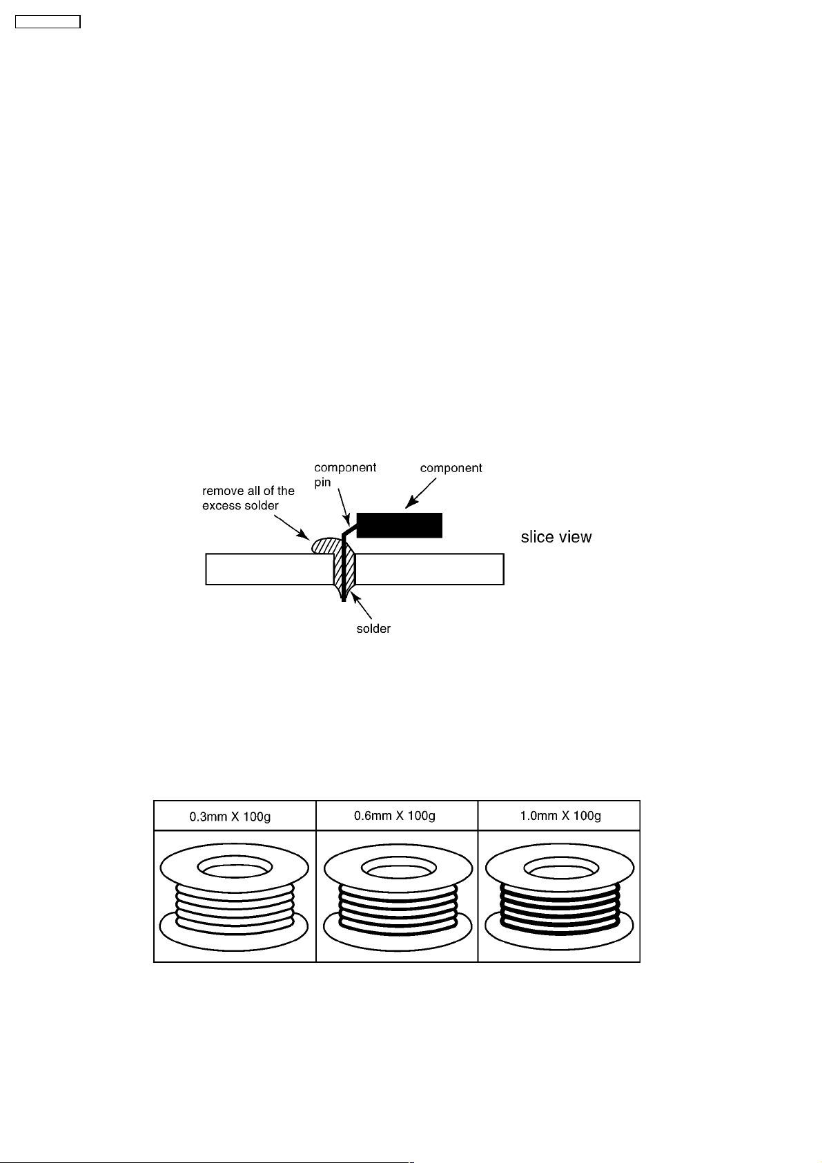
• When applying PbF solder to double layered boards, please check the component side for excess which may flow onto the
opposite side (See the figure below).
1.1. Suggested PbF Solder
There are several types of PbF solder available commercially. While this product is manufactured using Tin, Silver, and Copper
(Sn+Ag+Cu), you can also use Tin and Copper (Sn+Cu), or Tin, Zinc, and Bismuth (Sn+Zn+Bi). Please check the manufac
turer’s specific instructions for the melting points of their products and any precautions for using their product with other
materials.
The following lead free (PbF) solder wire sizes are recommended for service of this product: 0.3mm, 0.6mm and 1.0mm.
4
Page 5

1.2. How to recognize that Pb Free Solder is Used
(Example: Handset P.C.B.)
PROGRAM
LOUD
12
GND OUTPUT
MIC
RINGER
PAUSE
CH
7
4
LED703
8
0
LED704
9
#
LED702
5
LED705
6
FLASH LED701
1
2
3
TALK
REDIAL
PbF
AUTO
DIRECT
DTCOUT
R843
C866
C864
PSAVE
C839
C838
R848
C848
TXVCO
C861
R837
Q804
R838
R841
C862
C860
R839
C858
C836
C804
C832
R802
C831
Marked
Note:
The location of the "PbF" mark is subject to change without notice.
2 FOR SERVICE TECHNICIANS
ICs and LSIs are vulnerable to static electricity.
When repairing, the following precautions will help prevent recurring malfunctions.
1. Cover plastic parts boxes with aluminum foil.
2. Ground the soldering irons.
3. Use a conductive mat on worktable.
4. Do not grasp IC or LSI pins with bare fingers.
KX-TC2105LBB
TXPOWER
1
C852
6431
6
C865
Q802
C854
C870
C857
R830
R835
C855
R836
C863
R804
Q803
C808
R834
433
C805
1
C873
3
C872
C851
4
R831
R833
C856
664
R801
1
SP+ SP-
C853
NDTC
GND
IFOUT
R803
C803
Q801
C802
C801
ANT_TP
IFGND
R851
C871
R850
RXVCO
3 CAUTION
1. Danger of explosion if battery is incorrectly replaced.
2. Replace only with the same or equivalent type recommended by the manufacturer.
3. Dispose of used batteries according to the manufacturer´s Instructions.
5
Page 6
KX-TC2105LBB
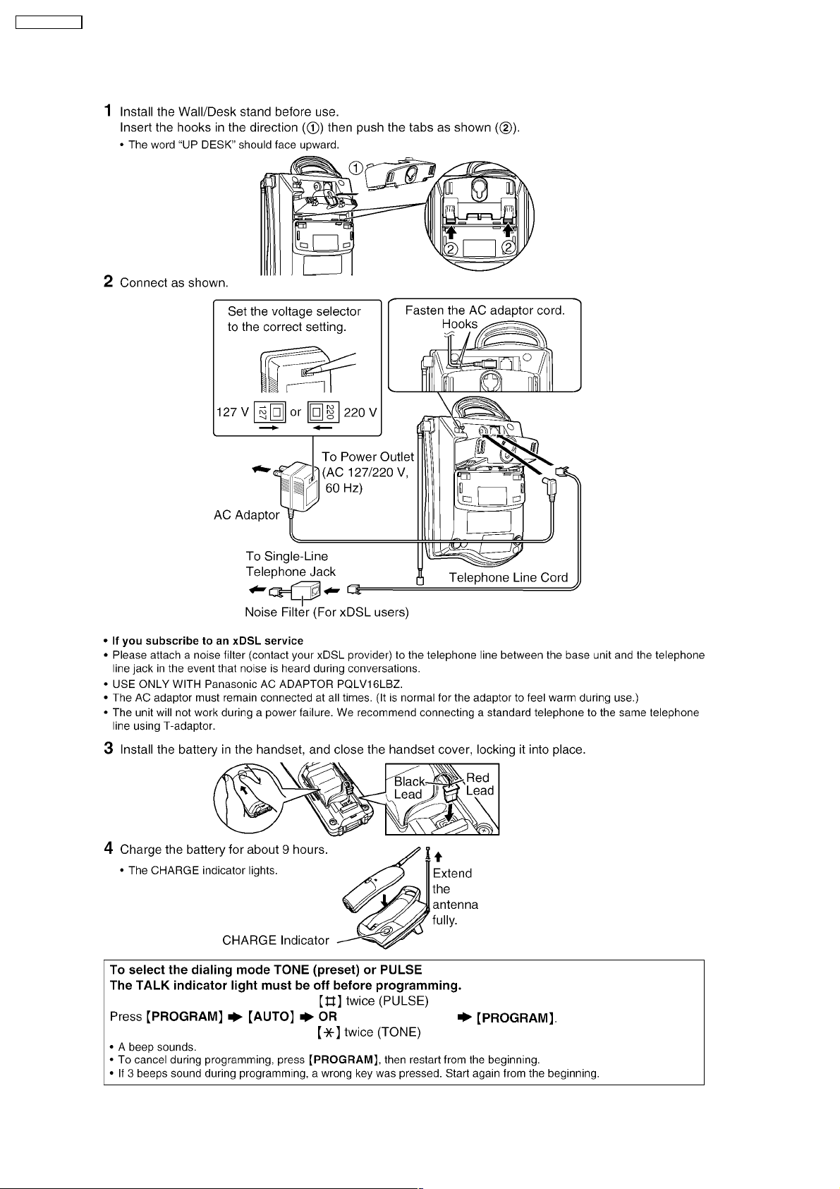
4 OPERATING INSTRUCTIONS
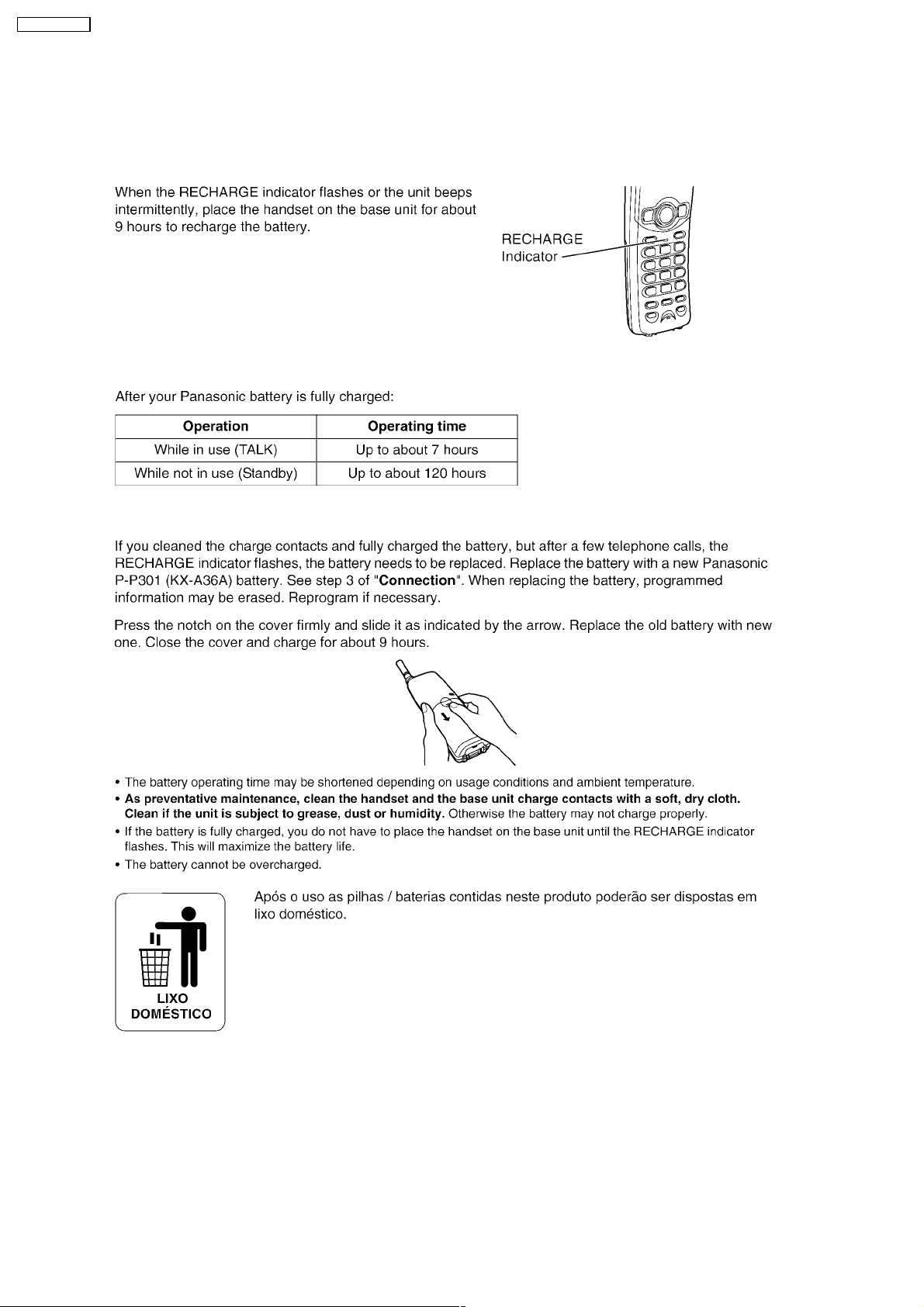
4.1. Battery
4.1.1. Recharge
4.1.2. Battery information
4.1.3. Battery Replacement
6
Page 7
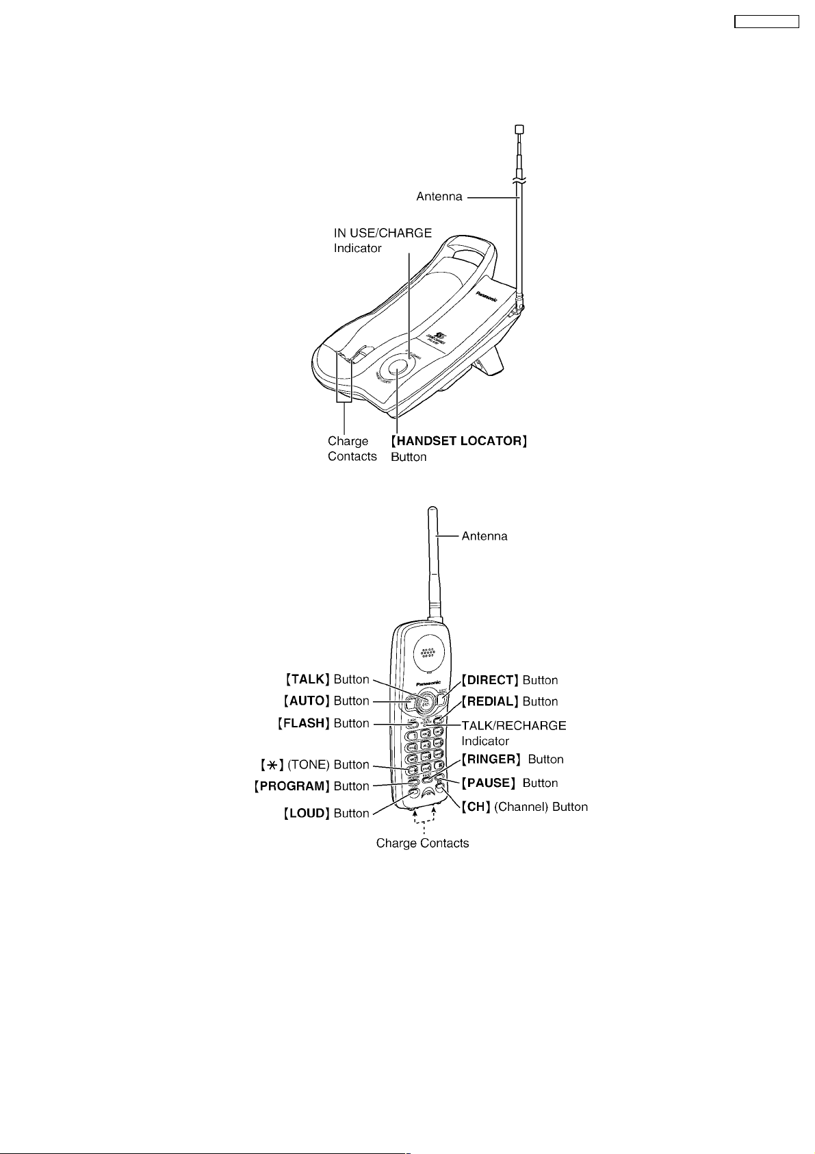
4.2. Location of Controls
4.2.1. Base Unit
KX-TC2105LBB
4.2.2. Handset
7
Page 8
KX-TC2105LBB
4.3. Connection
8
Page 9
4.4. Troubleshooting
KX-TC2105LBB
9
Page 10
KX-TC2105LBB
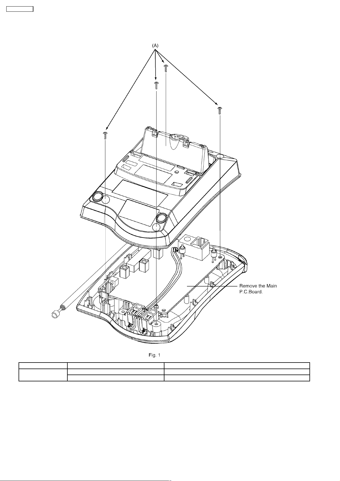
5 DISASSEMBLY INSTRUCTIONS
Shown in Fig.- To Remove Remove
1 Cabinet Cover Screws (2.6 × 12)....................... (A) × 4
Main P.C. Board Main P.C. Board
10
Page 11
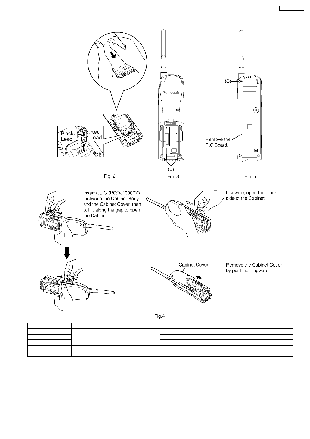
KX-TC2105LBB
Shown in Fig.- To Remove Remove
2 Cabinet Cover Battery compartment cover.
3 Screws (2.6 × 12)......................(B) × 2
4 Follow the procedure.
5 Main P. C. Board Screw (2.6 × 12)........................(C) × 1
Main P. C. Board
11
Page 12

KX-TC2105LBB
6 TROUBLESHOOTING GUIDE
Cross Reference:
Check Power (P.13)
Bell Reception (P.14)
Check Battery Charge (P.15)
Check Link (P.16)
Check Handset Transmission (P.17)
Check Handset Reception (P.18)
12
Page 13
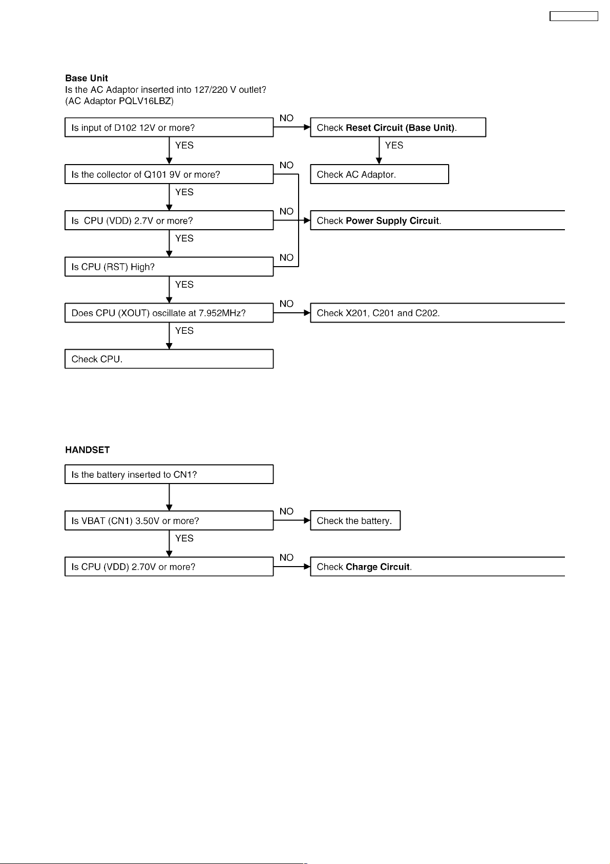
6.1. Check Power
KX-TC2105LBB
Cross Reference:
Reset Circuit (P.34)
Power Supply Circuit (P.33)
Cross Reference:
Charge Circuit (P.35)
*: Each measurement points are shown in CIRCUIT BOARD (BASE UNIT) (P.59) or CIRCUIT BOARD (HANDSET) (P.61)
Note:
*CPU: IC201
Note:
*CPU: IC701
13
Page 14
KX-TC2105LBB
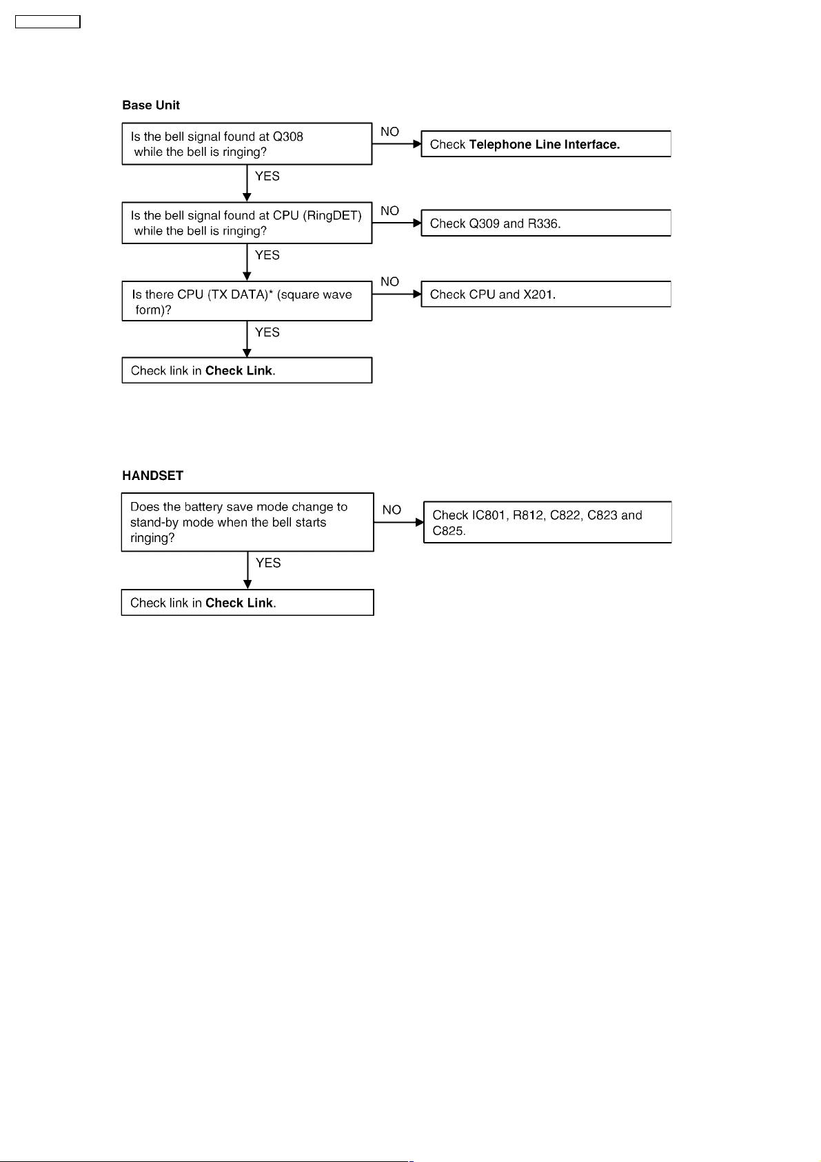
6.2. Bell Reception
Cross Reference:
Check Link (P.16)
Telephone Line Interface (P.35)
Cross Reference:
Check Link (P.16)
*: Each measurement points are shown in CIRCUIT BOARD (BASE UNIT) (P.59) or CIRCUIT BOARD (HANDSET) (P.61)
Note:
*CPU: IC201
Note:
*CPU: IC701
14
Page 15

6.3. Check Battery Charge
KX-TC2105LBB
Cross Reference:
Charge Circuit (P.35)
Cross Reference:
Reset Circuit (P.39)
*: Each measurement points are shown in CIRCUIT BOARD (BASE UNIT) (P.59) or CIRCUIT BOARD (HANDSET) (P.61)
Note:
*CPU: IC201
Note:
*CPU: IC701
15
Page 16
KX-TC2105LBB
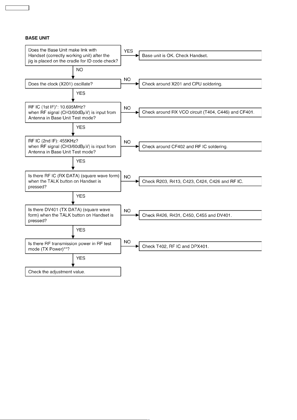
6.4. Check Link
**: Refer to Adjustment (P.20) Note:
*CPU: IC201
*RF IC: IC401
*: Each measurement points are shown in CIRCUIT BOARD (BASE UNIT) (P.59) or CIRCUIT BOARD (HANDSET) (P.61)
16
Page 17

KX-TC2105LBB
**: Refer to Adjustment (P.23). Note:
*CPU: IC701
*RF IC: IC801
*: Each measurement points are shown in CIRCUIT BOARD (BASE UNIT) (P.59) or CIRCUIT BOARD (HANDSET) (P.61)
6.5. Check Handset Transmission
Cross Reference:
SIGNAL ROUTE (P.41)
17
Page 18

KX-TC2105LBB
6.6. Check Handset Reception
Cross Reference:
SIGNAL ROUTE (P.41)
18
Page 19
7 ADJUSTMENTS (BASE UNIT)
If your unit has below symptoms, adjust or confirm each item using remedy column from the table.
Symptom Remedy*
The base unit does not respond to a call from handset. Make adjustments in item (A)
The base unit does not transmit or the transmit frequency is off. Make adjustments in item (B)
The transmit frequency is off. Make confirmation in item (C)
The transmit power output is low, and the operating distance between the base unit and
the handset is less than normal.
The reception sensitivity of base unit is low with noise. Make confirmation in item (E)
The transmit level is high or low. Make confirmation in item (F)
The reception level is high or low. Make confirmation in item (G)
The unit does not link. Make confirmation in item (H)
*: Refer to Adjustment (P.20).
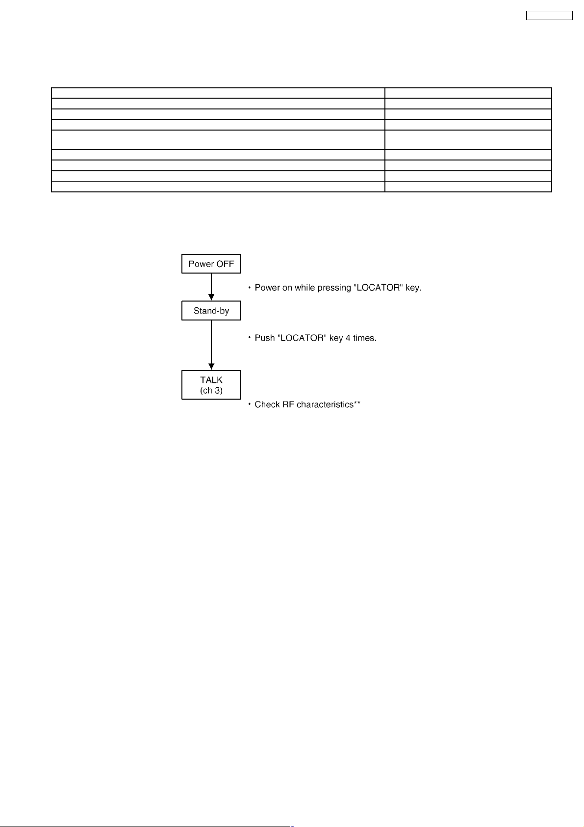
7.1. Test Mode Flow Chart (Base Unit)
The operation-flow of Test mode and main check items are shown below.
Make adjustments in item (D)
KX-TC2105LBB
Note:
**: Refer to the above table.
19
Page 20

KX-TC2105LBB
7.2. How to change the channel
Note:
Refer to Adjustment Standard (Base Unit) (P.21) for connection.
7.3. Adjustment
Adjustment Items Test Mode Adjustment
(A) RX VCO
Adjustment
(B) TX VCO
Adjustment
(C) TX Frequency
Confirmation
(D) TX Power
Adjustment
(E) RX Sensitivity
Confirmation (2nd
IF output)
(F) Line Output Level
Confirmation
(G) Line Input
Modulation
Confirmation
(H) Noise Squelch
Confirmation
3ch Talk T404
3ch Talk T402
3ch Talk -
3ch Talk T403
3ch Talk T401 1. Apply -60dBm output from S.S.G. (modulation frequency 1KHz, dev.
3ch Talk - 1. Apply -60dBm output from S.S.G. (modulation frequency 1KHz, dev.
3ch Talk - 1. Input via loop simulator 1.0KHz, 55mV (measured at T-R) signal.
3ch Talk - 1. Measure the S.S.G. output level when the noise squelch changes from
Point
*Procedure Check or
• Adjust T404 so that the reading of the Digital Voltmeter is 1.5 ± 0.3 V.
• Adjust T402 so that the reading of the Digital Voltmeter is 0.8 ± 0.3 V.
• Confirm so that the reading of the frequency counter is 43.820MHz ±
700Hz.
• Adjust T403 so that the reading of the RF VTVM is more than -8dBm.
0KHz).
2. Confirm that the reading of AF VTVM is the maximum value (more than
20mV).
3KHz).
2. Confirm that the reading of AF VTVM is more than 250mV (600Ω load).
2. Apply -60dBm output from S.S.G. (modulation frequency 1KHz, dev.
0KHz).
3. Confirm so that the reading of FM Deviation Meter is 2.0 ± 0.5KHz.
Low to High.
2. Confirm that the S.S.G. output level is -95dBm ~ -100dBm.
Replace
Parts
IC401, T404,
C446
IC401,
DV401,
T402
IC401, X401,
DV401,
C440,
C441
IC401, Q403,
Q405, T403,
DPX401
DPX401,
T401,
CF401,
CF402
IC401, Q304
IC401,
DV401
IC401,
DPX401
* : The connections of adjustment equipment are as shown in Adjustment Standard (Base Unit) (P.21).
S.S.G. Frequency: 48.86 MHz
20
Page 21

KX-TC2105LBB
CH-UP
GND2
C306
R221
R222
R320
R224
GND3
R308
R318
R319
C314
Q305
CH_UP
R223
C203
R226
R323
33
34
R305
C315
R225
R227
C313
R321
R236
C321
R317
R322
R228
R304
C310
23
R333
22
44
R229
R303
R310
C309
C205
R230
RING
TIP
C307
R313
R207
IC201
1
R231
R302
C206
RING
C305
R311
TP7
R435
C204
R209
Loop
Simulator
600ohm
PbF
R337
R312
Q402
R208
R215
R216
R217
11 12
R205
R232
R210
TIP
R427
R206
R233
C201
R234
C452
R428
SQL
C208
C450
R426
R235
PWR_GND
SA303
Q309
C455
C451
C449
C202
R203
R202
Q202
PWR_GND
C101
R425
C445
R334
C323
R336
R431
C463
C439
5VREG
PDown
DC 12V
DC12V
C322
R102
R103
R335
R110
C461
R433
TXVCO
R421
R422
C448
C475
C441
R420
C437
C436
DC12V
CH+
C453
R429
3
R424
1
R423
C440
C433
Q201
R105
R436
C434
1
C438
R106
Q104
R439
R430
4
6
RXVCO
C442
R419
R417
RXDT
R109
Q403
C457
C446
C432
R441
C447
C430
R418
R108
C454
C474
Q404
435642
14
R416
R315
C468
C458
R432
IC401
R316
CH-
R107 R443
Q405
R442
C456
C408
15
R434
R405
C429
C428
C467
R437
C465
C409
C311
3
1
3
1
C466
C464
C426
C424
C427
R211
C103
C412
C425
C470
R438
C410
C459
29
28
R411
R412
C471
R440
4
6
C411
C423
C420
C207
4
6
9.1VREG
R402
R447
C416
C415
DET
C419
R410
R413
R444
R415
TP2
C472
RXGND
RXANT
C405
C406
C414
R408
GND1
C105
R403
1
6
R446
R407
C418
C421
LOCATOR
TXGND
C473
Q401
R404
R409
R406
C404
IFOUT
C417
C422
R204
TP6
TP1
C402
R401
R445
3
4
LED201
C403
TXANT
C407
IFGND
GND
TXANT
(A)
RXVCO
(C)
Frequency Counter
RXGND
DC Volt Meter
IFGND
IFOUT
(D)
Spectrum Analyzer
RF Signal Generator
Audio Analyzer
TXGND
RXANT
DC Volt Meter
(B)
TXVCO
RF Volt Meter
7.4. Adjustment Standard (Base Unit)
When connecting the Simulator and Equipments for checking, please refer to the illustration below.
(G)
Oscilloscope
Note: (A) - (G) is referred to ADJUSTMENTS (BASE UNIT) (P.19)
21
Page 22

KX-TC2105LBB
8 ADJUSTMENTS (HANDSET)
If your unit has below symptoms, adjust or confirm each item using remedy column from the table.
Symptom Remedy*
The movement of Battery Low Indicator is wrong. Make confirmation in item (A)
The base unit does not respond to a call from the handset. Make adjustments in item (B)
The base unit does not transmit or the transmit frequency is of f. Make adjustments in item (C)
The transmit frequency is off. Make confirmation in item (D)
The transmit power output is low, and the operating distance between the base unit and
the handset is less than normal.
The reception sensitivity of the handset is low with noise. Make confirmation in item (F)
Does not link between the base unit and the handset. Make confirmation in item (G)
The reception level is high or low. Make confirmation in item (H)
The transmit level is high or low. Make confirmation in item (I)
*: Refer to Adjustment (P.23).
Unit condition:
1. Remove the antenna lead wire from P.C. Board of the handset.
2. Power Supply: DC 3.9V (DC power supply)
3. Volume: HIGH (When P.C. Board of handset is in test mode, volume condition is medium. Press “LOCATOR” key once.)
4. Speaker Load: 150Ω
CH TX Frequency RX Frequency
CH3 48.860MHz 43.820MHz
Make adjustments in item (E)
8.1. Test Mode Flow Chart (Handset)
Note:
Refer to CIRCUIT BOARD (HANDSET) (P.61)
SIGNAL ROUTE (P.41)
22
Page 23

8.2. How to change the channel
8.3. Adjustment
KX-TC2105LBB
Adjustment Items Test Mode Adjustment
(A) Battery Low
Confirmation
(B) TX VCO
Adjustment
(C) RX VCO
Adjustment
(D) TX Frequency
Confirmation
(E) TX Power
Adjustment
(F) RX Sensitivity
Confirmation
(2nd IF output)
(G) Noise Squelch
Confirmation
(H) Speaker
Output Level
Confirmation
(I) Mic Modulation
Factor
Confirmation
(J) Data
Modulation
Confirmation
3ch Talk - 1. Adjust the power supply voltage to DC 3.60V and confirm so that the
3ch Talk T803
3ch Talk T804
3ch Talk -
3ch Talk T802
3ch Talk T801 1. Apply -60dBm output from S.S.G. (modulation frequency 1KHz, dev.
3ch Talk - 1. Measure the S.S.G. output level when the noise squelch changes from
3ch Talk - 1. Apply -60dBm output from S.S.G. (modulation frequency 1KHz, dev.
3ch Talk - 1. Apply a MIC signal (1KHz, 4mV at 600Ω load).
3ch Talk -
Point
*Procedure Check or
reading of oscilloscope is High.
2. Adjust that power supply voltage to DC 3.40V and confirm so that the
reading of oscilloscope is Low.
• Adjust T803 so that the reading of the Digital Voltmeter is 0.8 ± 0.3 V.
• Adjust T804 so that the reading of the Digital Voltmeter is 1.0 ± 0.3 V.
• Confirm so that the reading of the frequency counter is 48.860MHz ±
700Hz.
• Adjust T802 so that the reading of the RF VTVM is more than -5dBm.
0KHz).
2. Confirm 2nd IF output so that the reading of AF VTVM is the maximum
value(more than 20mV).
Low to High. (modulation frequency 1KHz, dev.3KHz)
2. Confirm that the S.S.G. output level is -100dBm.
3KHz).
2. Confirm that the reading of AF VTVM is more than 30mV
(Distortion:less than 7%) (volume High)
2. Confirmation so that the reading FM Deviation Meter is 2.2 ± 0.5KHz.
• Confirm for 4KHz ~ 7KHz FM Deviation Meter reading.
Replace
Parts
IC801
IC801, X801,
T803, DV1
IC801, X801,
T804,C831
IC801,
DPX1,
T802
IC801, Q802,
Q804, T802,
DPX1
DPX1, T801,
CF801,
CF802
IC801, DPX1
IC801
IC801, DV1
Q802, Q804,
T802, DV1,
DPX1
*: The connections of adjustment equipment are as shown in Adjustment Standard (Handset) (P.24).
S.S.G. Frequency: 43.82 MHz
23
Page 24

KX-TC2105LBB
(H)
(A), (G)
Modulation Meter
RF Signal Generator
(I), (J)
Spectrum Analyzer
(E)
GND
Audio Analyzer
SP-
SP+
NDTC
C872
C873
TXPOWER
(D)
C853
C851
4
3
R831
C852
1
6
C854
Q802
6
43
C865
C870
1
C861
Q804
R837
Frequency Counter
R848
C864
C866
R843
DTCOUT
AUTO
GND
R833
R830
C857
R838
C848
R841
C855
R835
C862
C860
C802
IFOUT
C856
R836
C863
R839
C858
Oscilloscope
ANT_TP
C801
IFGND
R803
R834
Q803
R804
C808
C832
C836
C804
PSAVE
R851
C803
R802
C871
6
C839
R850
R801
311
C831
C838
Q801
C805
3
644
DIRECT
RXVCO
TXVCO
(C)
IFGND
DC Volt Meter
RXVCO
(B)
IFGND
DC Volt Meter
TXVCO
(F)
TALK
IFGND
DC Power Supply
FLASH LED701
REDIAL
RF Volt Meter
IFOUT
1
4
7
PROGRAM
+
LOUD
-
2
LED702
5
8
LED703
0
RINGER
12
GND OUTPUT
MIC
LED705
LED704
3
6
9
PbF
#
PAUSE
CH
8.4. Adjustment Standard (Handset)
When connecting the Simulator and Equipments for checking, please refer to the illustration below.
Note: (A)-(J) is referred to ADJUSTMENTS (HANDSET) (P.22)
24
Page 25

9 RF SPECIFICATION
9.1. Base Unit
Item Value Refer to -.* Remarks
TX Frequency 43.820 MHz ± 700 Hz ADJUSTMENTS (BASE UNIT) (C) at CH3
TX Power more than -8dBm ADJUSTMENTS (BASE UNIT) (D) at CH3
Line Modulation factor 2.0 KHz ± 0.5 KHz ADJUSTMENTS (BASE UNIT) (G)
Data Modulation factor 5.5 KHz ± 1.5 KHz —
Line Output level more than 250 mV —
*: Refer to Adjustment (P.20).
9.2. Handset
Item Value Refer to -.** Remarks
TX Frequency 48.860 MHz ± 700 Hz ADJUSTMENTS (HANDSET) (D) at CH3
TX Power more than -5dBm ADJUSTMENTS (HANDSET) (E) at CH3 (Antenna
soldering point 50Ω
Load)
Data Modulation factor 5.5 KHz ± 1.5 KHz ADJUSTMENTS (HANDSET) (J) at CH3
MIC Modulation factor 2.2 KHz ± 0.5 KHz ADJUSTMENTS (HANDSET) (I) at CH3 (MIC terminal
4mV Input)
SP Output level more than 30 mV —
KX-TC2105LBB
**: Refer to Adjustment (P.23).
10 HOW TO CHECK THE HANDSET SPEAKER
1. Prepare the digital voltmeter, and set the selector knob to ohm meter.
2. Put the probes at the speaker terminals as shown below.
25
Page 26

KX-TC2105LBB
11 FREQUENCY TABLE (MHz)
BASE UNIT HANDSET
Channel Transmit Frequency Receive Frequency Transmit Frequency Receive Frequency
1 43.720 48.760 48.760 43.720
2 43.740 48.840 48.840 43.740
3 43.820 48.860 48.860 43.820
4 43.840 48.920 48.920 43.840
5 43.920 49.020 49.020 43.920
6 43.960 49.080 49.080 43.960
7 44.120 49.100 49.100 44.120
8 44.160 49.160 49.160 44.160
9 44.180 49.200 49.200 44.180
10 44.200 49.240 49.240 44.200
11 44.320 49.280 49.280 44.320
12 44.360 49.360 49.360 44.360
13 44.400 49.400 49.400 44.400
14 44.460 49.460 49.460 44.460
15 44.480 49.500 49.500 44.480
16 46.610 49.670 49.670 46.610
17 46.630 49.845 49.845 46.630
18 46.670 49.860 49.860 46.670
19 46.710 49.770 49.770 46.710
20 46.730 49.875 49.875 46.730
21 46.770 49.830 49.830 46.770
22 46.830 49.890 49.890 46.830
23 46.870 49.930 49.930 46.870
24 46.930 49.990 49.990 46.930
25 46.970 49.970 49.970 46.970
26
Page 27

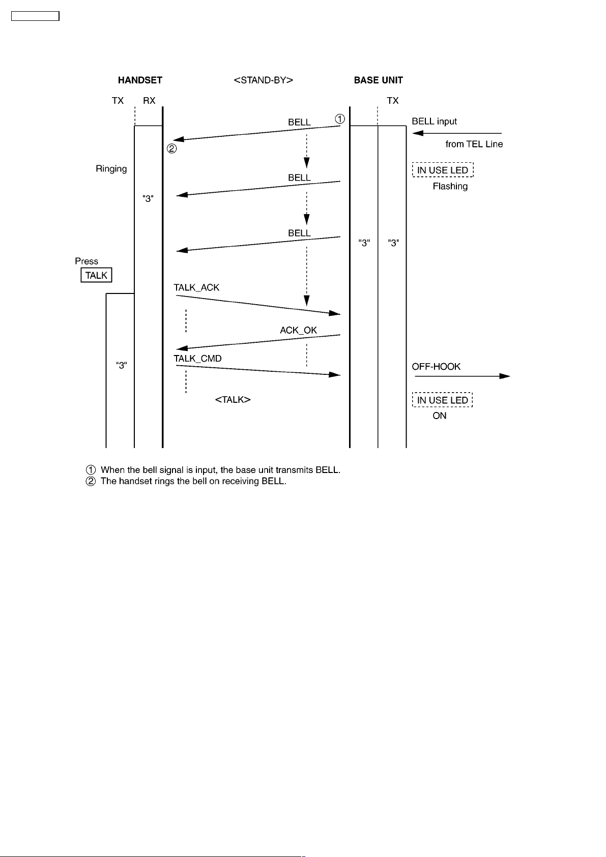
12 EXPLANATION OF CPU DATA COMMUNICATION
12.1. STAND-BY -> TALK, TALK -> STAND-BY
KX-TC2105LBB
*: The channel is changed if the noise interferes with the conversation.
27
Page 28
KX-TC2105LBB
12.2. Ringing
28
Page 29

12.3. Changing the Channel
KX-TC2105LBB
29
Page 30

KX-TC2105LBB
12.4. Ports for transmitting and receiving of data
Handset:
transmitting (TX) ... 25 Pin
receiving (RX) ... 12 Pin
Base Unit:
transmitting (TX) ... 23 Pin
receiving (RX) ... 10 Pin
12.5. Waveform of DATA used for cordless transmission and reception
The DATA which is transmitted from the Handset to the Base Unit is combination of DATA 0, DATA 1, DATA Delimit.
The DATA which is transmitted from the Base Unit to the Handset is combination of DATA 0, DATA 1, DATA Delimit.
12.5.1. Handset
12.5.2. Base Unit
• For example (one of part of data)
30
Page 31

TEL LINE
BELL DTC
D303-D306
Diode Bridge
Q309
DC 12V
Transistor
Q101,D103
KX-TC2105LBB
-
+
Q102,Q103
Charge Control
DATA Filter
Filter
PRE AMP
EXPANDER
AMP Q305
Q301,Q302
TEL LINE SW
TEL LINE
AMP Q304
LINE AMP
DATA AMP
DC9.1V
RESET
DOWN
POWER
MCU
RX DATA
RESET
RF EN
RF DATA
POWER DOWN
RF CLOCK
DC5V
CPU
LED201Q201
IC201
Q104
Charge Control
Charge Detection
KX-TC2105 BLOCK DIAGRAM (BASE UNIT)
2nd IF
Filter
Filter
1st IF
DPX401
DUPLEXER
13 BLOCK DIAGRAM (BASE UNIT)
IF Filter DET
1st Mixer 2nd Mixer
RF AMP
Q401,T401
RF IC
1st Local
RX VCO
T404,C446
IC401
Osc
Crystal
PLL
MIC AMP
LIMITER
COMPRESSOR
RX PD
TX PD
MODULATION
DV401
TX VCO
Q403,T402,
TX AMP
Q405,T403
31
Crystal
TX DATA
Page 32

KX-TC2105LBB
14 CIRCUIT OPERATION (BASE UNIT)
14.1. Outline
Base unit consists of the following ICs as shown in BLOCK DIAGRAM (BASE UNIT) (P.31).
• CPU: IC201
− Controlling the whole system
− Forming/analyzing all data signals (ACK, CMD signal etc.)
− All interfaces (ex: LED, Detector Circuit (Charge/ Power Down))
• RF IC: IC401
− PLL Oscillator
− Detection
− Compress/ Expander
− 1st/2nd mixer
− Amplifier for transmission and reception
− DC 5.5V regulator
− Reset Circuit
• Additionally,
− Power Supply Circuit
− Charge Circuit
− Telephone Line Interface Circuit
32
Page 33

14.2. Power Supply Circuit
The power supply to the CPU and RF IC from AC Adaptor (+12V) is shown in the diagram below.
The base unit power supply is DC12V. The handset power is supplied from DC 3.6V battery (Nickel-Cadmium battery) which
is installed in the handset.
Power supply for transmitter is turned on by pressing "TALK" key on the handset. During the stand-by mode, the unit stops
transmitting but receives the signal.
During on-hook condition (the handset is placed on the base unit), backup power for memory of the last dialed number is
supplied through the battery (DC 3.6V Nickel-Cadmium in the handset). The memory of this unit is not backed up by the current
from the telephone line.
The base unit DC power supply is regulated by Q101, D103. The CPU power is supplied from IC401. IC401 detects AC Adaptor
power failure and maintains the unit security code.
KX-TC2105LBB
<Fig. 1>
33
Page 34

KX-TC2105LBB
14.3. Reset Circuit
After power supply from AC adaptor, the reset signal for CPU is making in IC401. Refer to the below waveform.
<Fig. 2>
<Fig. 3>
34
Page 35

14.4. Charge Circuit
Circuit Operation:
When charging the handset on the base unit, the charge current is as follows;
DC12V → L101 → D102 → L103 → CH+(Base) → +CONTACT J601(Handset) → L602 → D602 → CN1-1 → Battery →
CN1-2 → -CONTACT J602(Handset) → CH-(Base) → L104 → Q102 → R104
In this way, the CPU on both units detects the fact that the battery is charged.
The charge current is controlled by switching Q103 of Base Unit. The battery is charged in normal mode for 9 hours and then
in trickle mode.
14.5. Telephone Line Interface
Function:
• Bell signal detection
• ON/OFF hook and pulse dial circuit
• Side tone circuit
Bell signal detection and OFF HOOK circuit:
In the idle mode, Q301 is open to cut the DC loop current and decrease the ring load. When ring voltage appears at the Tip (T)
and Ring (R) leads (When the telephone rings), the AC ring voltage is transferred as follows:
• JK1 TIP → P0301 → L301 → R334 → C322 → Q309 → IC201 Pin30
• JK1 RING → L302 → R333 → C321 → C323 → Q309 → IC201 Pin30
When the CPU detects a ring signal and press the “TALK” key on the handset, Q302 turns on and then Q301 turns on,
thus providing an off-hook condition (active DC current flow through the circuit) and the following signal flow is for the loop
current.
• Tip → P0301 → L301 → D303 → Q301 → R303 → Q302 → D306 → L302 → Ring
ON HOOK Circuit:
Q302 is open, Q301 is disconnected as to cut the DC loop current and to cut the voice signal. The unit is consequently in an
on-hook condition.
Pulse Dial Circuit:
CPU (Hook) turns Q302 ON/OFF to make the pulse dialing via Q301.
Make/Break ratio when dialing with the Handset 32% : 68%
Side Tone Circuit:
Basically this circuit prevents the TX signal from feeding back to RX signal.
As for this unit, TX signal feed back from Q304 is canceled by the side tone circuit C312, C313, R317, R318 and R319.
KX-TC2105LBB
35
Page 36

KX-TC2105LBB
14.6. Transmitter/Receiver
Base Unit and Handset mainly consist of RF (Radio Frequency) IC and CPU.
Base Unit and Handset transmit/receive voice signal and data signal through the antenna on carrier frequency.
Signal Path:
*Refer to CDL TX/RX in SIGNAL ROUTE (P.41).
14.6.1. Base to Handset
Circuit Operation:
The voice signal input from the TEL LINE interface goes to RF IC as shown in BLOCK DIAGRAM (BASE UNIT) (P.31).
In the talk mode (off-hook) condition, the telephone line voice signal passes through D303, Q301, C313, R320 and C315.
The signal goes through the compressor of RF IC, and it is output to transmitter circuit.
The signal of the data sent to the handset is applied in the anode of the variable capacitor diode (VARICAP : DV401).
The capacitor of VARICAP is changing in accordance with the voice signal from telephone line interface or TX DATA signal from
CPU. Therefore, the carrier frequency which is generated by TX VCO will be changed, and Frequency modulated RF
signal is generated and amplified by RF AMP (Q405, T403). It passes through the Duplexer DPX401 and is radiated from
Antenna.
The signal is transmitted from the base unit and received by the handset antenna and amplified by RF amplifier (Q801) through
DPX1 as shown in BLOCK DIAGRAM (HANDSET) (P.38). And then it is converted to 10.695 MHz and 455 KHz Intermediate
frequency by RF IC and related components.
The demodulated audio signal is output from RF IC (DET OUT) and passed through "Expander" process to reduce noise, then
voice signal amplified by "Receiver amplifier" is output to receiver (REC1).
The receiver loudness is adjustable by using "LOUD" key on the handset.
TX data (to Handset):
CPU (VTX) becomes low to turn on the transmission power transistor Q805, and CPU (TX-data) sends data signal. It is
FM-modulated by TX VCO and driven by RF AMP, then transmitted to the handset.
14.6.2. Handset to Base
Circuit Operation:
The voice signal from the handset user is picked up by the microphone (MIC), then it passes through "Compressor"
process to reduce noise as shown in BLOCK DIAGRAM (HANDSET) (P.38). And the voice is FM-modulated by
VARICAP (DV1).
The carrier frequency is generated by TX VCO. The transmitter power transistor Q805 is turned on/off by CPU (VTX).
The carrier signal is amplified by RF AMP and sent to the handset duplexer and antenna.
The signal of 49 MHz band (48.760~49.990) which is input from ANT is filtered at DPX401 as shown in
BLOCK DIAGRAM (BASE UNIT) (P.31), then it is input to RF IC.
The signal input to RF IC is converted through Mixer inside of RF IC, RF filter (CF1, CF2) and Expander.
The signal is transmitted from the handset and received by the base unit antenna and amplified by RF amplifier Q401, then
it is converted to10.695 MHz and 455 KHz Intermediate by RF IC. The demodulated audio signal is output from RF IC
(DET OUT) and passed through "Expander" process to reduce noise, then voice signal is led to LINE AMP. The signal passes
through TELEPHONE INTERFACE and Tel-line.
RX data (from Handset):
The data signal from handset (ex: Talk, ACK, COM) is also included in 49 MHz band same as the voice data. After second if
filter, the data signal is made square shape by data limiting AMP of the RF IC. RX data is output to CPU (RX Data).
36
Page 37

14.6.3. RF signal operation/control and PLL operation (RF UNIT)
Base unit radio frequency signal received by antenna passes through duplexer (DPX401).
RF signal is amplified by RF AMP. RF signal received from RF IC is mixed with RX local frequency at Mixer to generate
10.695 MHz wide band IF. The reference frequency is generated by X801 10.240 MHz crystal.
The 10.695 MHz is mixed with reference and 455 KHz narrow band IF is generated.
RF IC is controlled by CPU (RF EN, RF DATA, RF CLOCK). The RX local frequency is generated by RX VCO.
KX-TC2105LBB
37
Page 38

KX-TC2105LBB
DC3.9V
Battery
+
-
Filter
2nd IF
DATA Filter
Filter
PRE AMP
EXPANDER
IF Filter DET
SPEAKER
DATA AMP
SPEAKER AMP
RF IC
IC801
LIMITER
MIC
DOWN
POWER
MCU
MIC AMP
RX DATA
RF EN
RF CLOCK
RF DATA
POWER DOWN
Crystal
TX DATA
Reset
CPU
IC701
Key Matrix
Q704
Q705
Charge Detection
KX-TC2105 BLOCK DIAGRAM (HANDSET)
Buzzer
Q701,Q702
Filter
1st IF
RF AMP
DPX1
DUPLEXER
15 BLOCK DIAGRAM (HANDSET)
1st Mixer 2nd Mixer
1st Local
RX VCO
Q801,T801
Osc
Crystal
T804,C831
PLL
COMPRESSOR
TX PD
RX PD
MODULATION
DV1
TX VCO
Q804,T803,
TX AMP
Q802,T802
38
Page 39

16 CIRCUIT OPERATION (HANDSET)
16.1. Outline
Handset consists of the following ICs as shown in BLOCK DIAGRAM (HANDSET) (P.38).
• CPU: IC701
− Forming/analyzing all data signals (ACK or CMD signal)
− All interfaces (ex; LED, Key, Buzzer, Detector Circuit, Charge/Battery Low)
− RAM for keeping the data (CH Number, ID Code, etc.)
• RF IC: IC801
− PLL Oscillator
− Detection
− Compress/Expander
− 1st/2nd mixer
− Amplifier for transmission and reception
16.2. Reset Circuit
The power of handset is supplied by battery.
Whenever the battery is recharged or inserted, the impulse at CHG+ becomes Reset signal through Q704, and it is sent to CPU.
KX-TC2105LBB
<Fig. 4>
<Fig. 5>
39
Page 40

KX-TC2105LBB
16.3. Battery Low / Power Down Detector
Circuit Operation:
“Battery Low” and “Power Down” are detected by RF IC which check the voltage from battery. Shortly, every detected blocks
are inside of RF IC. The detected voltage is as follows;
• Battery Low
Battery voltage : V(Batt) < 3.457V
The CPU detects the level and “Recharge battery” LED starts flashing.
• Power Down
Battery voltage : V(Batt) < 3.0V
The output of RF IC (Power Down) becomes low level, then CPU stops working to keep the data (CH number, ID Code, etc.)
<Fig. 6>
40
Page 41

17 SIGNAL ROUTE
Each signal route is as follows.
KX-TC2105LBB
41
Page 42

KX-TC2105LBB
18 CPU DATA (Base Unit)
18.1. IC201
42
Page 43

19 CPU DATA (Handset)
19.1. IC701
KX-TC2105LBB
43
Page 44

KX-TC2105LBB
20 RF IC (Base Unit and Handset)
20.1. Base Unit: IC401, Handset: IC801
44
Page 45

21 HOW TO REPLACE THE FLAT PACKAGE IC
Even if you do not have the special tools (for example, a spot heater) to remove the Flat IC, with some solder (large amount),
a soldering iron and a cutter knife, you can easily remove the ICs that have more than 100 pins.
21.1. PREPARATION
• PbF (: Pb free) Solder
• Soldering Iron
Tip Temperature of 700°F ± 20°F (370°C ± 10°C)
Note: We recommend a 30 to 40 Watt soldering iron. An expert may be able to use a 60 to 80 Watt iron where someone with
less experience could overheat and damage the PCB foil.
• Flux
Recommended Flux: Specific Gravity → 0.82.
Type → RMA (lower residue, non-cleaning type)
Note: See ABOUT LEAD FREE SOLDER (PbF: Pb free) (P.4)
21.2. FLAT PACKAGE IC REMOVAL PROCEDURE
1. Put plenty of solder on the IC pins so that the pins can be completely covered.
Note:
If the IC pins are not soldered enough, you may give pressure to the P.C. board when cutting the pins with a cutter.
KX-TC2105LBB
2. Make a few cuts into the joint (between the IC and its pins) first and then cut off the pins thoroughly.
3. While the solder melts, remove it together with the IC pins.
When you attach a new IC to the board, remove all solder left on the land with some tools like a soldering wire. If some solder is
left at the joint on the board, the new IC will not be attached properly.
45
Page 46

KX-TC2105LBB
21.3. FLAT PACKAGE IC INSTALLATION PROCEDURE
1. Temporarily fix the FLAT PACKAGE IC, soldering the two marked pins.
*Check the accuracy of the IC setting with the corresponding soldering
foil.
2. Apply flux to all pins of the FLAT PACKAGE IC.
3. Solder the pins, sliding the soldering iron in the direction of the arrow.
21.4. BRIDGE MODIFICATION PROCEDURE
1. Lightly resolder the bridged portion.
2. Remove the remaining solder along the pins using a soldering iron as shown in the figure below.
46
Page 47

22 CABINET AND ELECTRICAL PARTS (BASE UNIT)
KX-TC2105LBB
47
Page 48

KX-TC2105LBB
23 CABINET AND ELECTRICAL PARTS (HANDSET)
48
Page 49

24 ACCESSORIES AND PACKING MATERIALS
KX-TC2105LBB
49
Page 50

KX-TC2105LBB
25 TERMINAL GUIDE OF THE ICs, TRANSISTORS AND
DIODES
25.1. Base Unit
25.2. Handset
50
Page 51
26 REPLACEMENT PARTS LIST
KX-TC2105LBB
1. RTL (Retention Time Limited)
Note:
The marking (RTL) indicates that the Retention Time is
limited for this item.
After the discontinuation of this assembly in production,
the item will continue to be available for a specific period
of time. The retention period of availability is dependant
on the type of assembly, and in accordance with the
laws governing part and product retention. After the end
of this period, the assembly will no longer be available.
2. Important safety notice
Components identified by the
mark indicates special
characteristics important for safety. When replacing any of
these components, only use specified manufacture’s parts.
3. The S mark means the part is one of some identical parts.
For that reason, it may be different from the installed part.
4. ISO code (Example: ABS-94HB) of the remarks column
shows quality of the material and a flame resisting grade
about plastics.
5. RESISTORS & CAPACITORS
Unless otherwise specified;
All resistors are in ohms (Ω) K=1000Ω, M=1000kΩ
All capacitors are in MICRO FARADS (µF)P=µµF
*Type & Wattage of Resistor
26.1. Base Unit
26.1.1. Cabinet and Electrical Parts
Ref.
No.
1 PQQT23004Z LABEL, CHARGE
2 PQKM10675Z1 CABINET BODY PS-HB
3 PQHR11113Z OPTIC CONDUCTIVE PARTS, LED
4 PQBC10428Z1 BUTTON, LOCATOR ABS-HB
5 PQSA10105Y ANTENNA
6 PQJT10229Z CHARGE TERMINAL
7 PQHR11115Z CASE, CHARGE TERMINAL PS-HB
8 PQKF10666Z1 CABINET COVER PS-HB
9 PQHA10030Z RUBBER PARTS, FOOT RUBBER
Part No. Part Name & Description Remarks
LENDS
PS-HB
Ref.
No.
10 PQGT18241Z NAME PLATE
11 PQQT23081Z LABEL, CAUTION
Part No. Part Name & Description Remarks
26.1.2. Main P.C.Board Parts
Note:
(*1) When you have replaced IC401, adjust X401. Refer to
ADJUSTMENTS (BASE UNIT) (P.19).
Ref.
No.
PCB1 PQWPC2105LBH MAIN P.C.BOARD ASS´Y (RTL)
IC201 MN101C94AKA IC
IC401 AN6266FA IC (*1)
Q101 B1AADE000014 TRANSISTOR(SI)
Q102 B1AADE000014 TRANSISTOR(SI)
Q103 B1AADE000014 TRANSISTOR(SI)
Q104 B1ABDE000020 TRANSISTOR(SI)
Q201 B1GBCFGG0028 TRANSISTOR(SI)
Q202 B1ABDE000020 TRANSISTOR(SI)
Q301 B1BCBR000013 TRANSISTOR(SI)
Q302 PQVT2N6517CA TRANSISTOR(SI) S
Q304 B1AAJC000010 TRANSISTOR(SI)
Q305 B1ABDE000020 TRANSISTOR(SI)
Q309 B1ABDE000020 TRANSISTOR(SI)
Q401 B1ABDE000020 TRANSISTOR(SI)
Q402 B1GDCFNN0021 TRANSISTOR(SI)
Q403 B1ABDE000020 TRANSISTOR(SI)
Q405 B1ABDE000020 TRANSISTOR(SI)
D101 MA4300 DIODE(SI) S
D102 B0EAKP000126 DIODE(SI)
D103 MA4100 DIODE(SI) S
D105 MA4300 DIODE(SI) S
D201 B0EAAD000001 DIODE(SI)
D303 B0EAKP000126 DIODE(SI)
D304 B0EAKP000126 DIODE(SI)
D305 B0EAKP000126 DIODE(SI)
D306 B0EAKP000126 DIODE(SI)
D307 MA4180 DIODE(SI) S
D308 B0EAAD000001 DIODE(SI)
D401 B0EAAD000001 DIODE(SI)
DV401 B0CAAB000021 DIODE(SI)
LED201 PQVDSML310MT LED S
L101 G0C100K00039 COIL
L104 PQLQZM100K COIL S
L301 PQLQZK3R3K COIL S
L302 PQLQZK3R3K COIL S
L401 PQLQZK1R5K COIL S
T401 G2BRC0000008 COIL
T402 PQL04B001 COIL
T403 G2BRC0000007 COIL
T404 PQL04B002 COIL
CF401 J0B1075A0127 CERAMIC FILTER
CF402 J0B4553A0065 CERAMIC FILTER
DPX401 J0E4535A0001 IC FILTER
X201 H0D795400007 CRYSTAL OSCILLATOR
X401 H0D102500029 CRYSTAL OSCILLATOR (*1)
JK1 K2LD104A0001 JACK S
SA302 J0LF00000026 VARISTOR (SURGE ABSORBER) S
SA303 J0LF00000048 VARISTOR (SURGE ABSORBER)
Part No. Part Name & Description Remarks
(ICs)
(TRANSISTORS)
(DIODES)
(COILS)
(CERAMIC FILTERS)
(IC FILTERS)
(CRYSTAL OSCILLATORS)
(JACKS)
(VARISTORS)
(RESISTORS)
51
Page 52
KX-TC2105LBB
Ref.
No.
R101 ERDS2TJ221 220
R102 ERJ3GEYJ102 1K
R103 ERJ3GEYJ102 1K
R104 ERDS2TJ151 150
R105 ERJ3GEYJ102 1K
R106 ERJ3GEYJ391 390
R107 PQ4R10XJ101 100 S
R108 PQ4R10XJ270 27 S
R109 ERJ3GEYJ103 10K
R110 ERJ3GEYJ104 100K
R202 ERJ3GEYJ103 10K
R203 ERJ3GEYJ104 100K
R204 ERJ3GEYJ681 680
R205 ERJ3GEYJ104 100K
R206 ERJ3GEYJ104 100K
R207 ERJ3GEYJ102 1K
R208 ERJ3GEYJ103 10K
R209 ERJ3GEYJ104 100K
R210 ERJ3GEYJ823 82K
R211 ERJ3GEY0R00 0
R215 ERJ3GEYJ472 4.7K
R216 ERJ3GEYJ472 4.7K
R217 ERJ3GEYJ472 4.7K
R223 ERJ3GEY0R00 0
R225 ERJ3GEY0R00 0
R230 ERJ3GEY0R00 0
R234 ERJ3GEY0R00 0
R235 ERJ3GEY0R00 0
R302 PQ4R10XJ104 100K S
R303 PQ4R10XJ472 4.7K S
R305 ERJ3GEYJ472 4.7K
R311 PQ4R10XJ821 820 S
R312 PQ4R10XJ103 10K S
R314 ERDS1TJ680 68
R315 ERJ3GEYJ223 22K
R317 ERJ3GEYJ222 2.2K
R318 ERJ3GEYJ222 2.2K
R319 ERJ3GEYJ181 180
R320 ERJ3GEYJ123 12K
R321 ERJ3GEYJ224 220K
R322 ERJ3GEYJ152 1.5K
R323 ERJ3GEYJ221 220
R333 PQ4R10XJ104 100K S
R334 PQ4R10XJ104 100K S
R335 PQ4R10XJ472 4.7K S
R336 ERJ3GEYJ473 47K
R337 PQ4R10XJ222 2.2K S
R401 ERJ3GEYJ561 560
R402 ERJ3GEYJ101 100
R403 ERJ3GEYJ392 3.9K
R404 ERJ3GEYJ470 47
R405 ERJ3GEYJ331 330
R406 ERJ3GEYJ103 10K
R407 ERJ3GEYJ184 180K
R408 ERJ3GEYJ392 3.9K
R409 ERJ3GEYJ223 22K
R410 ERJ3GEYJ333 33K
R412 ERJ3GEYJ823 82K
R413 ERJ3GEYJ153 15K
R415 ERJ3GEYJ274 270K
R416 ERJ3GEYJ334 330K
R417 ERJ3GEYJ393 39K
R418 ECUV1H222KBV 0.0022
R419 ERJ3GEYJ823 82K
R420 ERJ3GEYJ473 47K
R421 ERJ3GEYJ103 10K
R422 ERJ3GEYJ682 6.8K
R423 ERJ3GEYJ222 2.2K
R424 ERJ3GEYJ103 10K
R425 ERJ3GEYJ184 180K
R426 ERJ3GEYJ155 1.5M
R427 ERJ3GEYJ105 1M
R428 ERJ3GEYJ105 1M
Part No. Part Name & Description Remarks
Ref.
No.
R429 ERJ3GEYJ223 22K
R430 ERJ3GEYJ104 100K
R431 ERJ3GEYJ152 1.5K
R432 ERJ3GEYJ153 15K
R433 ERJ3GEYJ103 10K
R434 ERJ3GEYJ332 3.3K
R435 ERJ3GEYJ330 33
R436 ERJ3GEYJ101 100
R441 ERJ3GEYJ154 150K
R442 ERJ3GEYJ222 2.2K
R443 ERJ3GEYJ820 82
R444 ERJ3GEY0R00 0
R445 ERJ3GEYJ472 4.7K
R446 ERJ3GEY0R00 0
C102 ECEA1EKA100 10
C103 ECUV1H103KBV 0.01
C104 ECEA1CK101 100 S
C105 ECUV1H103KBV 0.01
C201 ECUV1H220JCV 22P
C202 ECUV1H220JCV 22P
C203 ECUV1E223KBV 0.022
C204 ECUV1C393KBV 0.039
C205 ECUV1H392KBV 0.0039
C206 ECUV1H391JCV 390P
C207 ECUV1C104KBV 0.1
C208 ECUV1H103KBV 0.01
C209 ECEA0JU471 470
C301 ECKD2H681KB 680P S
C303 ECKD2H681KB 680P S
C304 ECKD2H681KB 680P S
C305 PQCUV1H472KB 0.0047
C308 ECEA1HKS220 22 S
C309 PQCUV1H101JC 100P
C310 PQCUV1H103KB 0.01
C311 ECUV1A105KBV 1
C312 ECEA1HKA3R3 3.3
C313 ECUV1E153KBV 0.015
C314 ECUV1H272KBV 0.0027
C315 ECUV1H103KBV 0.01
C321 PQCUV1H154KR 0.15
C322 PQCUV1H154KR 0.15
C323 PQCUV1A684KB 0.68
C401 ECKERS102MB 0.001 S
C404 ECUV1H100DCV 10P
C407 ECUV1H103KBV 0.01
C408 ECUV1H103KBV 0.01
C409 ECUV1H103KBV 0.01
C410 ECUV1C104KBV 0.1
C411 ECUV1C104KBV 0.1
C412 ECUV1C104KBV 0.1
C413 ECEA1EKA100 10
C414 ECUV1C104KBV 0.1
C415 ECUV1H680JCV 68P
C416 ECUV1C104KBV 0.1
C417 ECUV1H121JCV 120P
C418 ECUV1H121JCV 120P
C419 ECUV1H103KBV 0.01
C420 ECUV1H471JCV 470P S
C421 ECUV1H153KBV 0.015
C422 ECJ1VB1H682K 0.0068
C423 ECUV1C104KBV 0.1
C424 ECUV1E223KBV 0.022
C425 ECUV1C104KBV 0.1
C426 ECUV1C473KBV 0.047
C427 ECUV1H103KBV 0.01
C428 ECJ1VC1H271J 270P
C429 ECUV1H152KBV 0.0015
C430 ECUV1H103KBV 0.01
C431 ECEA1CKA470 47
C432 ECUV1H103KBV 0.01
C433 ECJ1VC1H271J 270P
C434 ECUV1C683KBV 0.068
Part No. Part Name & Description Remarks
(CAPACITORS)
52
Page 53

KX-TC2105LBB
Ref.
No.
C435 ECEA1CKS220 22 S
C436 ECUV1H103KBV 0.01
C437 ECUV1H152KBV 0.0015
C438 ECJ1VC1H151J 150P
C439 ECUV1C104KBV 0.1
C440 ECUV1H430GCV 43P
C441 ECUV1H270GCV 27P
C442 ECUV1H103KBV 0.01
C443 ECEA1EKA100 10
C444 ECEA1HKA4R7 4.7
C445 ECUV1C224KBV 0.22
C446 ECUV1H180JCV 18P
C447 ECUV1H103KBV 0.01
C448 ECUV1H103KBV 0.01
C449 ECUV1H223KBV 0.022
C450 ECUV1H103KBV 0.01
C451 ECUV1H821KBV 820P
C452 ECUV1H102KBV 0.001
C453 ECUV1C104KBV 0.1
C454 ECUV1H470JCV 47P
C455 ECJ1VB1H682K 0.0068
C457 ECUV1H330JCV 33P
C458 ECUV1H390JCV 39P
C459 ECUV1H390JCV 39P
C460 ECEA1CKS220 22 S
C461 ECUV1H102KBV 0.001
C462 ECEA1CKA470 47
C463 ECUV1H100DCV 10P
C466 ECUV1H060DCV 6P S
C468 ECUV1H103KBV 0.01
C469 ECEA1CKA470 47
C470 ECUV1H103KBV 0.01
C471 ECUV1H050CCV 5P
C472 ECUV1H102KBV 0.001
PO301 D4FAR1500003 THERMISTOR (POSISTOR)
SW201 K0H1BB000018 SPECIAL SWITCH
Part No. Part Name & Description Remarks
(OTHERS)
26.2. Handset
26.2.1. Cabinet and Electrical Parts
Ref.
No.
101 PQKM10676Z1 CABINET BODY ABS-HB
102 PQSA10170Z ANTENNA
103 PQSX10296N KEYBOARD SWITCH
104 PQHR11114Z OPTIC CONDUCTIVE PARTS, LED
105 L0AD02A00029 SPEAKER
106 PQJT10230Z CHARGE TERMINAL (L)
107 PQJT10231Z CHARGE TERMINAL (R)
108 PQHS10696Z SPACER, BUZZER SHEET
109 PQKF10667Z1 CABINET COVER ABS-HB
110 PQGT18242Z NAME PLATE
111 PQQT22966Z LABEL, CAUTION
112 PQXA36ASVC BATTERY
113 PQHE10161Z SPACER
114 PQKK10589Z1 LID, BATTERY COVER ABS-HB
26.2.2. Main P.C.Board Parts
Note:
(*1) When you have replaced IC801, adjust X801. Refer to
ADJUSTMENTS (HANDSET) (P.22).
Ref.
No.
PCB100 PQWPC2105LBR MAIN P.C.BOARD ASS´Y (RTL)
IC701 MN101C427AP IC
IC801 AN6265FA IC (*1)
Part No. Part Name & Description Remarks
LENS
Part No. Part Name & Description Remarks
(ICs)
(TRANSISTORS)
PS-HB
Ref.
No.
Q701 B1ADDE000022 TRANSISTOR(SI)
Q702 B1ABDE000020 TRANSISTOR(SI)
Q704 B1ABDE000020 TRANSISTOR(SI)
Q705 B1GBCFGJ0011 TRANSISTOR(SI)
Q801 B1ABDE000020 TRANSISTOR(SI)
Q802 B1ABDE000020 TRANSISTOR(SI)
Q804 B1ABDE000020 TRANSISTOR(SI)
Q805 B1GDCFNN0021 TRANSISTOR(SI)
D601 MA8056H DIODE(SI) S
D602 MA111 DIODE(SI) S
D701 B0ACCL000002 DIODE(SI)
DV1 B0CAAB000021 DIODE(SI)
LED701 PQVDSML310MT LED S
L603 PQLQZK1R0K COIL S
L801 PQLQZMR47K COIL S
T801 G2BRC0000006 COIL
T802 G2AYYYC00058 COIL
T803 PQL04B004 COIL
T804 G2AYYYC00060 COIL
CF1 J0B1075A0127 CERAMIC FILTER
CF2 J0B4553A0065 CERAMIC FILTER
X701 H0D399400013 CRYSTAL OSCILLATOR
X801 H0D102500029 CRYSTAL OSCILLATOR (*1)
DPX1 J0E4935A0001 IC FILTER
CN1 PQJP2D13Z CONNECTOR S
R701 ERJ3GEYJ334 330K
R702 ERJ3GEYJ104 100K
R703 ERJ3GEYJ334 330K
R705 ERJ3GEYJ102 1K
R706 ERJ3GEYJ104 100K
R707 ERJ3GEYJ331 330
R708 ERJ3GEYJ334 330K
R710 ERJ3GEY0R00 0
R712 ERJ3GEYJ102 1K
R713 ERJ3GEYJ222 2.2K
R714 ERJ3GEYJ104 100K
R715 ERJ3GEYJ151 150
R719 ERJ3GEY0R00 0
R729 ERJ3GEYJ222 2.2K
R730 ERJ3GEYJ222 2.2K
R731 ERJ3GEYJ222 2.2K
R801 ERJ3GEYJ823 82K
R802 ERJ3GEYJ820 82
R803 ERJ3GEYJ331 330
R804 ERJ3GEYJ821 820
R805 ERJ3GEYJ332 3.3K
R806 ERJ3GEYJ474 470K
R807 ERJ3GEYJ223 22K
R808 ERJ3GEYJ153 15K
R809 ERJ3GEYJ473 47K
R810 ERJ3GEYJ823 82K
R811 ERJ3GEYJ153 15K
R812 ERJ3GEYJ153 15K
R815 ERJ3GEYJ222 2.2K
R816 ERJ3GEYJ333 33K
R817 ERJ3GEYJ222 2.2K
R818 ERJ3GEYJ393 39K
R819 ERJ3GEYJ103 10K
R820 ERJ3GEYJ102 1K
R821 ERJ3GEY0R00 0
R822 ERJ3GEYJ822 8.2K
R823 ERJ3GEYJ123 12K
R824 ERJ3GEYJ223 22K
R825 ERJ3GEYJ222 2.2K
R826 ERJ3GEYJ184 180K
R827 ERJ3GEYJ223 22K
Part No. Part Name & Description Remarks
(DIODES)
(COILS)
(CERAMIC FILTERS)
(CRYSTAL OSCILLATORS)
(IC FILTERS)
(CONNECTOR AND JACK)
(RESISTORS)
53
Page 54

KX-TC2105LBB
Ref.
No.
R828 ECUV1H392KBV 0.0039
R829 ERJ3GEYJ222 2.2K
R830 ERJ3GEYJ222 2.2K
R831 ERJ3GEYJ104 100K
R832 ERJ3GEYJ221 220
R837 ERJ3GEYJ101 100
R838 ERJ3GEYJ393 39K
R839 ERJ3GEYJ122 1.2K
R841 ERJ3GEYJ473 47K
R842 ERJ3GEYJ473 47K
R843 ERJ3GEYJ102 1K
R844 ERJ3GEY0R00 0
R845 ERJ3GEYJ105 1M
R848 ERJ3GEYJ683 68K
R850 ERJ3GEY0R00 0
R851 ERJ3GEY0R00 0
R852 ERJ3GEYJ104 100K
C869 ERJ3GEY0R00 0
C874 ERJ3GEY0R00 0
C602 ECUV1C104KBV 0.1
C701 ECEA0JKA101 100
C702 ECUV1C104KBV 0.1
C703 ECUV1H220JCV 22P
C704 ECUV1H220JCV 22P
C705 ECUV1C473KBV 0.047
C706 ECUV1C104KBV 0.1
C707 ECUV1C104KBV 0.1
C708 ECUV1C104KBV 0.1
C803 ECUV1H100JCV 10P
C804 ECUV1H391JCV 390P S
C805 ECUV1H050CCV 5P
C807 ECUV1H103KBV 0.01
C808 ECUV1H103KBV 0.01
C809 ECUV1H103KBV 0.01
C810 ECUV1H103KBV 0.01
C811 ECUV1C104KBV 0.1
C812 ECUV1H680JCV 68P
C813 ECUV1C104KBV 0.1
C814 ECEA1CKA100 10
C815 ECUV1H121JCV 120P
C816 ECUV1H121JCV 120P
C817 ECUV1C104KBV 0.1
C818 ECUV1H471JCV 470P S
C820 ECUV1C473KBV 0.047
C821 ECJ1VB1H472K 0.0047
C822 ECUV1C104KBV 0.1
C823 ECUV1H103KBV 0.01
C824 ECUV1C473KBV 0.047
C825 ECUV1C104KBV 0.1
C826 ECUV1C104KBV 0.1
C827 ECUV1H103KBV 0.01
C828 ECUV1H103KBV 0.01
C829 ECUV1H103KBV 0.01
C830 ECUV1H103KBV 0.01
C831 ECUV1H220JCV 22P
C833 ECUV1C224KBV 0.22
C834 ECUV1H103KBV 0.01
C835 ECUV1C474KBV 0.47
C836 ECUV1C104KBV 0.1
C837 ECST0JY106 10 S
C838 ECUV1H270GCV 27P
C839 ECUV1H390GCV 39P
C840 ECUV1C104KBV 0.1
C841 ECUV1H820JCV 82P
C842 ECUV1H152KBV 0.0015
C843 ECUV1H103KBV 0.01
C844 ECUV1H101JCV 100P
C845 ECEA1CKA100 10
C846 ECUV1H103KBV 0.01
C847 ECUV1H123KBV 0.012
C848 ECUV1C104KBV 0.1
C850 ECUV1H103KBV 0.01
Part No. Part Name & Description Remarks
(CAPACITORS)
Ref.
No.
C852 ECUV1H100DCV 10P
C853 ECUV1H103KBV 0.01
C854 ECUV1H103KBV 0.01
C858 ECUV1H100DCV 10P
C859 ECEA1CKA100 10
C860 ECUV1H103KBV 0.01
C861 ECUV1H220JCV 22P
C862 ECUV1H390JCV 39P
C863 ECUV1H390JCV 39P
C864 ECUV1H390JCV 39P
C865 ECUV1H020CCV 2P
C866 ECUV1C333KBV 0.033
C867 ECUV1E223KBV 0.022
C868 ECUV1C104KBV 0.1
C870 ECUV1H150JCV 15P
C872 ECUV1H102KBV 0.001
C876 ECST0JY106 10 S
E101 PQEFBDB111GF BUZZER
E102 PQJM122Z MICROPHONE
Part No. Part Name & Description Remarks
(OTHERS)
26.3. Accessories and Packing
Materials
Note:
(*1) You can download and refer to the Operating
Instructions (Instruction book) on TSN Server.
Ref.
No.
A1 PQLV16LBZ AC ADAPTOR
A2 PQJA10075Z CORD, TELEPHONE
A3 PQQX14815Z INSTRUCTION BOOK (*1)
A4 PQQW14831Z LEAFLET
A5 PQKL10069Z1 STAND, WALL MOUNT ABS-HB
A6 PQQT23066Z LABEL, CORD
P1 PQPP10104Z PROTECTION COVER (for Base
P2 PQPP10105Z PROTECTION COVER (for
P3 PQPK14931Z GIFT BOX
Part No. Part Name & Description Remarks
Unit)
Handset)
54
Page 55

27 FOR SCHEMATIC DIAGRAM
27.1. Base Unit (SCHEMATIC DIAGRAM (BASE UNIT))
1. DC voltage measurements are taken with an oscilloscope or a tester with a ground.
2. The schematic diagrams and circuit board may be modified at any time with the development of new technology.
Important Safety Notice:
Components identified by
any of these components, use only the manufacturer´s specified parts.
27.2. Handset (SCHEMATIC DIAGRAM (HANDSET))
1. DC voltage measurements are taken with an oscilloscope or a tester with a ground.
2. The schematic diagrams and circuit board may be modified at any time with the development of new technology.
mark have special characteristics i mportant for safety. When replacing
KX-TC2105LBB
55
Page 56

KX-TC2105LBB
NC : No Components
KX-TC2105 SCHEMATIC DIAGRAM (Base Unit)
IC201
28 SCHEMATIC DIAGRAM (BASE UNIT)
IC401
56
Page 57

IC701
KX-TC2105LBB
NC : No Components
KX-TC2105 SCHEMATIC DIAGRAM (Handset)
29 SCHEMATIC DIAGRAM (HANDSET)
IC801
57
Page 58

KX-TC2105LBB
Memo
58
Page 59

KX-TC2105LBB
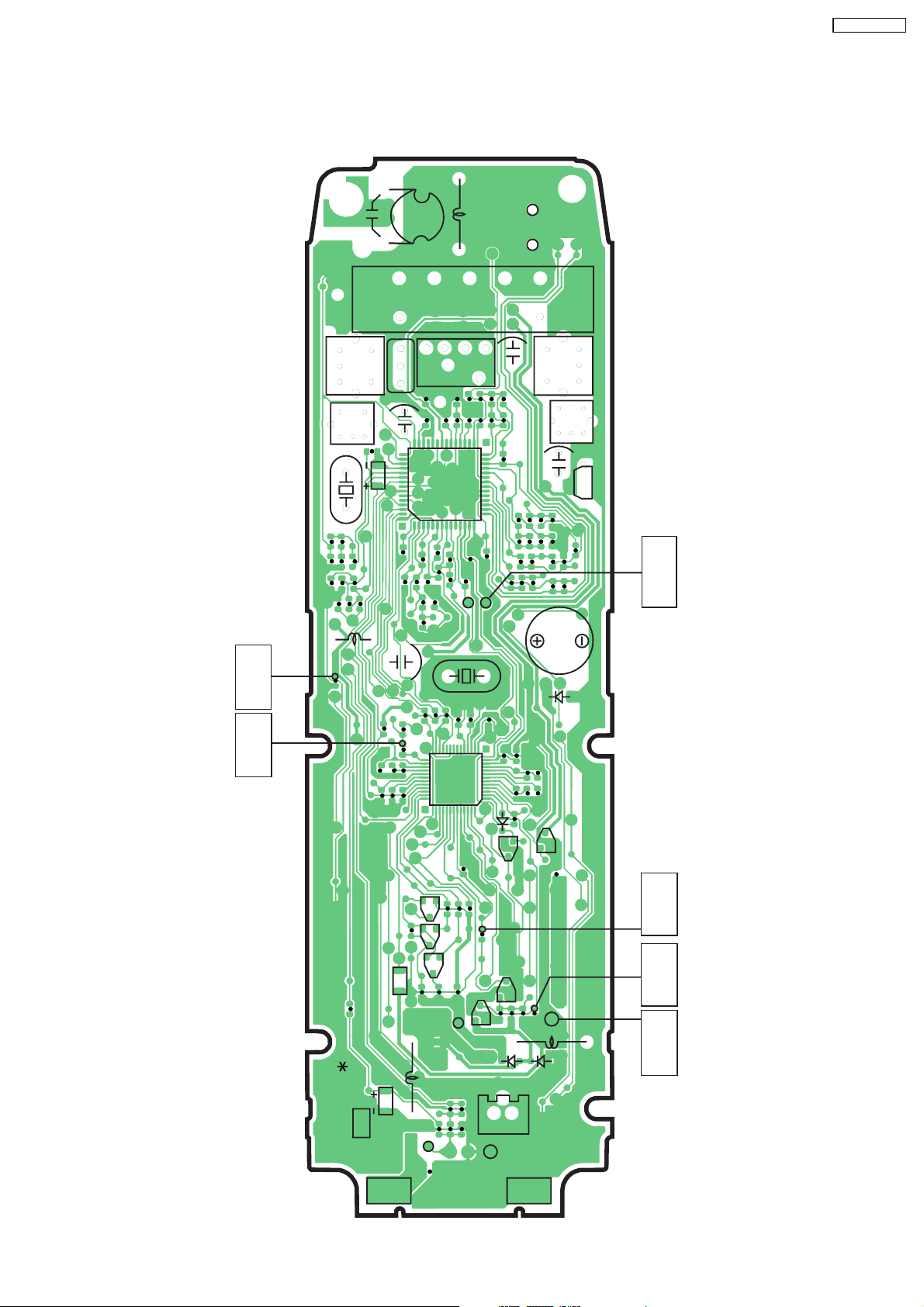
A
ANT1
C401
L401
1
2
3
45
3
4
12 3 4
SW201
C102
J33
C104
DPX401
1
T401
6
5
PQUP11346Z
CF402
D102
D103
D101
T403
64
J31
4
6
J24
C413
PbF
J21
R414
L102
L101
BC
Q101
E
R104
C469
13
3
T402
1
C431
J23
IN GND OUT
J6
R101
B
E
Q102
E
Q103
B
J32
CF401
C443
J19
R418
D104
D105
CH+
CH-
GND
L103
L104
C
C
C304
C462
C460
KA
DV401
C444
T404
64
13
J20
X401
J12
C435
J7
C209
J5
J3
SA301
C303
D308
J30
J13
D201
L201
JK1
J28
J34
J15
D305
J16
PO301
D306
E
C308
J26
J1
2
D304
C
Q301
D307
D401
J22
J36
J11
X201
1
D303
B
R314
J10
J2
B
B
J9
Q302
Q304
J4J27
J25
C301
R301
L301
C
C
J35
D301
C302
E
R306
E
J18
J14
R307
Q303
E
R309
C312
J37
C
J17
SA302
D302
L302
KX-TC2105 CIRCUIT BOARD (Base Unit (Component View))
B
J29
J8
30 CIRCUIT BOARD (BASE UNIT)
30.1. Component View
59
Page 60

KX-TC2105LBB
RING DET
(CPU: 30)
CHG DET
(CPU: 27)
TXDATA
(CPU: 23)
GND2
C306
R221
R222
R224
R320
GND3
R308
R318
R319
C314
Q305
CH_UP
R223
C203
R226
C315
R323
33
34
R305
C313
R321
R236
R225
R227
C321
R317
R322
R228
R304
C310
23
R333
R303
R310
22
44
R229
RING
C309
C205
IC201
1
R230
RING
TIP
R302
C307
R313
R207
R231
C305
R311
R435
C204
C206
TP7
R215
R209
TIP
PbF
R312
Q402
R208
R216
11 12
R205
R232
R210
R337
R427
R217
R206
R233
C452
R428
SQL
C201
C208
R234
C451
C450
R426
R202
R235
PWR_GND
PWR_GND
C101
SA303
Q309
C455
R425
C449
C445
C202
R203
Q202
R334
C323
R336
R431
C463
R422
C439
5VREG
PDown
R335
R421
C441
C437
DC12V
CH+
C322
R102
R103
R110
C461
R433
R429
TXVCO
C448
C475
R420
C436
DC 12V
R105
R106
Q104
R436
R439
C453
R430
3
R424
1
R423
RXVCO
C442
C440
1
C438
R419
C433
R417
C434
Q201
Q403
4
6
RXDT
R109
R441
C457
C447
C446
C430
C432
R418
R108
Q404
C454
C474
R315
C468
C458
R432
435642
IC401
14
R416
CH-
R107 R443
Q405
R442
C456
C408
15
R316
R437
C465
R434
R405
C429
C428
C467
3
1
C409
C311
C103
3
1
C466
C464
C412
C426
C425
C424
C427
R211
C470
R438
C459
C410
29
28
R411
R412
4
C471
6
R440
4
6
9.1VREG
C411
C423
C420
R413
C207
R402
C416
R410
R444
R415
R447
C415
DET
C419
GND1
C105
TP2
C472
RXGND
RXANT
C405
C406
R446
C414
C418
R408
TXGND
C473
R403
Q401
1
R404
6
IFOUT
R407
R409
R406
C421
LOCATOR
C404
C417
C422
R204
TP6
TP1
C402
R401
R445
3
4
C403
C407
LED201
TXANT
IFGND
TXPOWER
KX-TC2105 CIRCUIT BOARD (Base Unit (Flow Solder Side View))
TXGND
RXGND
TXVCO
RXANT
2ND MIX
(RFIC: 37)
RXVCO
IF GND
30.2. Flow Solder Side View
RESET
(CPU: 39)
CDD
(CPU: 13)
CHG LD
(CPU: 4)
XOUT
(CPU: 14)
60
RXDATA
(RFIC: 13)
DET OUT
(RFIC: 27)
IF OUT
(RFIC: 33)
Page 61
ANT2
KX-TC2105LBB
C806
VDD
(CPU: 14)
TXDATA
(CPU: 25)
ANT
T801
31
6
T804
1
C834
X801
R822
R819
C830
C833
C835
C827
C867
R821
L701
C708
5
OG
I
46
CF1
4
3
C845
4356
C837
C842
R820
C840
R823
R842
C701
R708
R845
R723
R725
R726
R727
R728
R715
42
1
R824
C869
C868
R724
Q701
1
C807
C841
C843
R731
36 25
4
C809
R825
R852
R844
R730
24
37
C811
C810
IC801
C844
R849
R729
R712
Q702
DPX1
CF2
R805
R826
C704
IC701
C705
R711
L801
3
4
5
C813
R807
C812
C824
29
28
15
14
C828
C846
R703
RXDT
PDOWN
X701
C703
C702
13
112
48
D702
Q706
R713
R705
C816
R806
2
R808
C815
C817
C826
R722
R718
R816
R809
C825
R701
C814
C820
C818
R815
R720
R717
R707
Q805
BLACK
RED
1
R811
R810
R812
R817
R721
4
6
C859
C821
C875
C822
C829
D701
R719
T802
6
1
C823
BZ1
C602
3
1
T803
R818
4
3
K
DV1
A
C874
KX-TC2105 CIRCUIT BOARD (Component View (Handset))
RXDATA
(RFIC: 13)
RESET
(CPU: 43)
31 CIRCUIT BOARD (HANDSET)
31.1. Component View
Q703
R704
KX-TC2100 series
R832
R710
R709
BAT1
L602
C876
PbF
PQUP11347Z
MIC1
J601 J602
R828
R829
C847
C601
Q705
R714
R706
R827
CN1
C850
21
MIC2
61
Q704
C706
C707
D601D602
VBAT
L603
R702
CHG DET
(CPU: 1)
VBAT
(RFIC: 36)
A
Page 62

KX-TC2105LBB
C873
TXPOWER
3
1
43
DTCOUT
C872
C852
AUTO
6
1
R843
SP+ SP-
C851
4
6
C861
C866
C853
R831
C865
R837
C864
TXPOWER
GND
NDTC
R833
C854
R830
Q802
C870
C857
Q804
R838
R841
R848
C848
C855
R835
C862
C860
IF OUT
C802
IFOUT
C856
R836
C863
R839
C858
(RFIC: 33)
ANT_TP
C801
IFGND
R803
R834
Q803
R804
C808
C836
PSAVE
IF GND
C871
R851
C803
6
C832
R802
C804
C839
R850
R801
C805
311
C831
C838
RXVCO
Q801
3
644
DIRECT
TXVCO
RXVCO
2ND MIX
(RFIC: 37)
TXVCO
KX-TC2105 CIRCUIT BOARD (Flow Solder Side View (HANDSET))
DC Power
Supply
+ -
TALK
FLASH LED701
1
LED702
4
7
LED703
PROGRAM
RINGER
12
GND OUTPUT
LOUD
REDIAL
2
3
LED705
5
8
0
LED704
6
9
PbF
#
PAUSE
CH
31.2. Flow Solder Side View
MIC
62
Page 63

KX-TC2105LBB
63
I.N./N
KXTC2105LBB
 Loading...