

Technical Guide
Colour Television
EURO 4 Chassis
Circuit Explanations
Order No. TZS8EL001
3DQDVRQLF
(XURSHDQ 7HOHYLVLRQ 'LYLVLRQ
0DWVXVKLWD (OHFWULF 8. /WG

3DQDVRQLF
CONTENTS
1. Introduction 3....................................................
2. Power Supply Block Diagram 4....................................
3. Control Block Diagram 5..........................................
4. Video Block Diagram 6............................................
5. Standard Audio Block Diagram 7...................................
6. Audio & Dolby Block Diagram 8....................................
7. Dolby Block Diagram 9............................................
8. Power Supply 10..................................................
9. Horizontal and Vertical Outputs 17...................................
10. A.F. Output Stage 21...............................................
11. Colour Output Stage 22............................................
12. RF/IF Section 25..................................................
13. Microprocessor and Teletext Processing 27...........................
14. EAROM Memory IC 37.............................................
15. EPROM 38.......................................................
16. Control Of The Digital Section 39....................................
17. Video Display Processor 40........................................
18. M-Board Processing 55............................................
19. AV Switching 57...................................................
20. Audio Signal Processing 58.........................................
21. History Of Dolby Pro Logic 67.......................................
22. Pro Logic Processing Overview 68..................................
23. Pro Logic Encoding and Decoding Concepts 69.......................
24. Dolby Pro Logic Processor (DPL3519A) 72...........................
25. C-Board Processing 80............................................
2

1. Introduction
We at Panasonic realise that the service engineer
needstounderstandthecircuitry insidetheTVandfor
this need, we have produced this Technical Guide.
This Technical Guide contains information for
EURO 4 chassis and should be used in-conjunction
3DQDVRQLF
with the relevant Service Manuals for this chassis.
As the TechnicalGuide forthe Euro 4 chassis covers
sucha wide rangeof models,some differencesoccur
in circuit descriptions and component reference
numbers. Where these differences occur they will be
highlighted by (
Italic text with brackets
).
3
odel Spec
c
3DQDVRQLF
3
4
3
6
2
2
353
5
3
odel Spec
c
odel Spec
c
2.
T2701
P
F
4
P
E115K2
77
E62
1 2
E81Y2
22V
S
18V
S
S
-18V
5
1
E - BOARD
Q852
D867
DEGAUSS
COIL
E1
D868
T802 RL801
4
1
2
1
Line
Filter
R802
Q853
E2
M
ifi
1
IC1051
4
M
l
ifi
REMOTE
CONTROL
RECEIVER
R805
-
D801
POWER
SUPPLY
R814
Q855
Q854
D805
5V
-14V
14V
200V
D454
E53C1
1
V-OUTPUT
6
3
T801
AUDIO
OUTPUT
1
29V
S
150
S
D850
7V
Q850
15V
1
IC851
REG
12V
TUNER
33V
R854
5V
5V
33V
D862
9
27V
EW
CORRECTION
REG
IC850
REG
IC107
REMOTE
CONTROL
RECEIVER
IC1104
RESET
N12E19
2
4
5V
IC1101
MICRO
PROCESSOR
IC1102
EPROM
1
8V
8
EAROM
5V
2
RESET
3
IC2101
Audio
Processor
RGB
6
R2714
Q2701
35
IC2702
K - BOARD
M
Q2701
4
7
Video
Switching
Video
Processor
Q2702
ifi
IC24048IC2403
Y - BOARD
R2715
H - BOARD
C - BOARD
M
5
6
IC2401
1
4
3
1 3
ifi
POWER SUPPLY BLOCK DIAGRAM
E - BOARD
3. CONTROL BLOCK DIAGRAM
5
H - BOARD
IC3401
VIDEO
SWITCHING
K - BOARD
IC2401
Dolby
Processor
N - BOARD
IC1071
REMOTE
CONTROL
RECEIVER
TUNER
H31E61
3
1
IC2101
4
AUDIO
PROCESSOR
8
7
SDA 1
SCL 1
SCL
SDA
IC601
4
VIDEO
PROCESSOR
3
SERVICE / TEST
E18
K23E11
4 4
N1
4
8 8
3
E19
SCL
SDA
48
49
VPROT
R.C.
L.E.D.
71
60
52
74
81
75
IC1101
MICROPROCESSOR
SCL 2
50
SDA 2
51
SLOW 2
58
OUT
72
IN
73
5955
IC1103
6
EAROM
5
LOCAL
KEYS
SWITCH
MATRIX
4
KEYSCAN
PROT 1
7
8
IC1051
REMOTE
CONTROL
RECEIVER
Model Specific
SLOW 1
SERVICE
6
5
4
3
AV2
8
10
AV1
8
10
12
SDA 1
SCL 1
SDA 2
SCL 2
SLOW 2
AV LINK
3DQDVRQLF
SLOW 1
SCL 1
SDA 1
7
7
odel Spec
c
3DQDVRQLF
4.
AV1
9LGHR2XW
%OXH
*UHHQ
5HG
9LGHR
E - BOARD
,Q
Q105
Q104
61 V IN
43 B IN
42 G IN
41 R IN
62 VIN 2
63 VIN 3
60 C IN
VIN 4
64
IC601
VIDEO
PROCESSOR
VIDEO OUT
59
SVM OUT 34
B OUT 39
G OUT 38
R OUT 37
B IN 47
G IN 46
R IN 45
Q950 Q951
Q30
Q30
Q301
Q302
E8
4
4
3
3
5
5
Y2
M
Q906
Q905 Q907 Q909
IC351
3
7
Q353
RGB
OUTPUT
2
1
8
9
Y - BOARD
ifi
Q908
VM
COILS
CRT
VIDEO BLOCK DIAGRAM
6
AV2
9LGHR
$9
,Q
&
Q3601
2XW
9LGHR
AV3
Q3001
68
CVBS
IC1101
MICRO
PROCESSOR
R 37
G 38
B 39
E15
H - BOARD
H1
6
6
8
8
1
1
Q3402
Q3401
IC3401
8
VIDEO
SWITCHING
6
5
H3E61
5
E - BOARD
TUNER
5 R
2 L
IC251
AUDIO
OUTPUT
R 7
L 11
IC2101
AUDIO
PROCESSOR
Model
Specific
X101
&
X102
Model
Specific
Q101
7
Q102
Q103
44 MONO IN
49 ANA_IN2+
47 ANA_IN1+
DACM_R 24
DACM_L 25
SC3_IN_L 37
SC3_IN_R 38
SC1_OUT_R 30
SC1_IN_R 42
SC1_OUT_L 31
SC1_IN_L 41
Q2102
Q252
Q2103
Q251
E6
1
E7
3
AV3
6 R
7 R
HEADPHONE
5 L
4 L
L
R
1 R OUT
2 R IN
3 L OUT
6 L IN
STANDARD AUDIO BLOCK DIAGRAM
Q2304
Q2302
Q2301
Q2303
21 DACA_R
22 DACA_L
SC2_OUT_R 27
SC2_IN_R 40
SC2_OUT_L 28
SC2_IN_L 39
AUDIO
MONITOR
OUT
AV1
1 R OUT
2 R IN
3 L OUT
6 L IN
3DQDVRQLF
Q103
Q
3DQDVRQLF
6. AUDIO & DOLBY BLOCK DIAGRAM
8
To K7
DACA_R
DACA_L
E - BOARD
Model Specific
E12
3
4
X101
OR
X102
TUNER
Q101
Model Specific
Q102
Q2304
Q2302
44 MONO IN
49 ANA_IN2+
47 ANA_IN1+
21 DACA_R
22 DACA_L
IC2101
I2S_DA_IN_2 18
I2S_DA_IN_1 12
I2S_DA_OUT 11
I2S_DA_WS 10
I2S_DA_CL 9
DACM_R 24
SC3_IN_L 37
SC3_IN_R 38
SC1_OUT_R 30
SC1_IN_R 42
SC1_OUT_L 31
SC1_IN_L 41
SC2_OUT_R 27
SC2_IN_R 40
SC2_IN_L 38
SC2_OUT_L 28
DACM_L 25
2102
Q2103
Q252
Q251
5 R
2 L
IC251
R 7
L 11
E12
3
4
5
6
7
E7
3
E6
1
E23
3
1
AV3
2 R
HEADPHONE
3 L
L
R
AV2
1 R OUT
2 R IN
3 L OUT
6 L IN
AV1
2 R IN
3 L OUT
6 L IN
To K3
I2S_DA_IN_2
I2S_DA_IN_1
I2S_DA_OUT
I2S_DA_WS
I2S_DA_CL
R
L
From K8
H_LEFT
H_RIGHT
7. DOLBY BLOCK DIAGRAM
Q2705
K-Board
Centre
Q2704
Q2703
IC2704
1
4
IC2703
K5
K6
C2
1
1
3
3
5
5
C5
1
1
Q2405
Q2423Q2422
Q2432 Q2425
Woofer
To E12 K3
I2S_WS
I2S_CL
3
4
5
6
7
9
I2S_DAOUT_2
I2S_DA_OUT_1
I2S_DA_IN
Audio Left
Audio Right
19
11
12
10
9
IC2401
Q2410
27
2221
Q2409
Q2403
24
25
Q2401
1
IC2402
3
5
7
Q2426 Q2428
Q2427 Q2424
Q2404
Q2402
14
12
10
8
Surround
1
1
Q2406
4
IC2702
4
C-Board
Q2419
Q2418
Q2417
Q2421
Q2420
JK2702
Surround L
Surround R
Centre
JK2401
Surround R
Surround L
Centre Out
Right Front
Left Front
JK2402
Woofer
3DQDVRQLF
To E22 K7
1
3
IC2404
13
57
K8 To E23
Headphone Right
1
3
Headphone Left
3DQDVRQLF
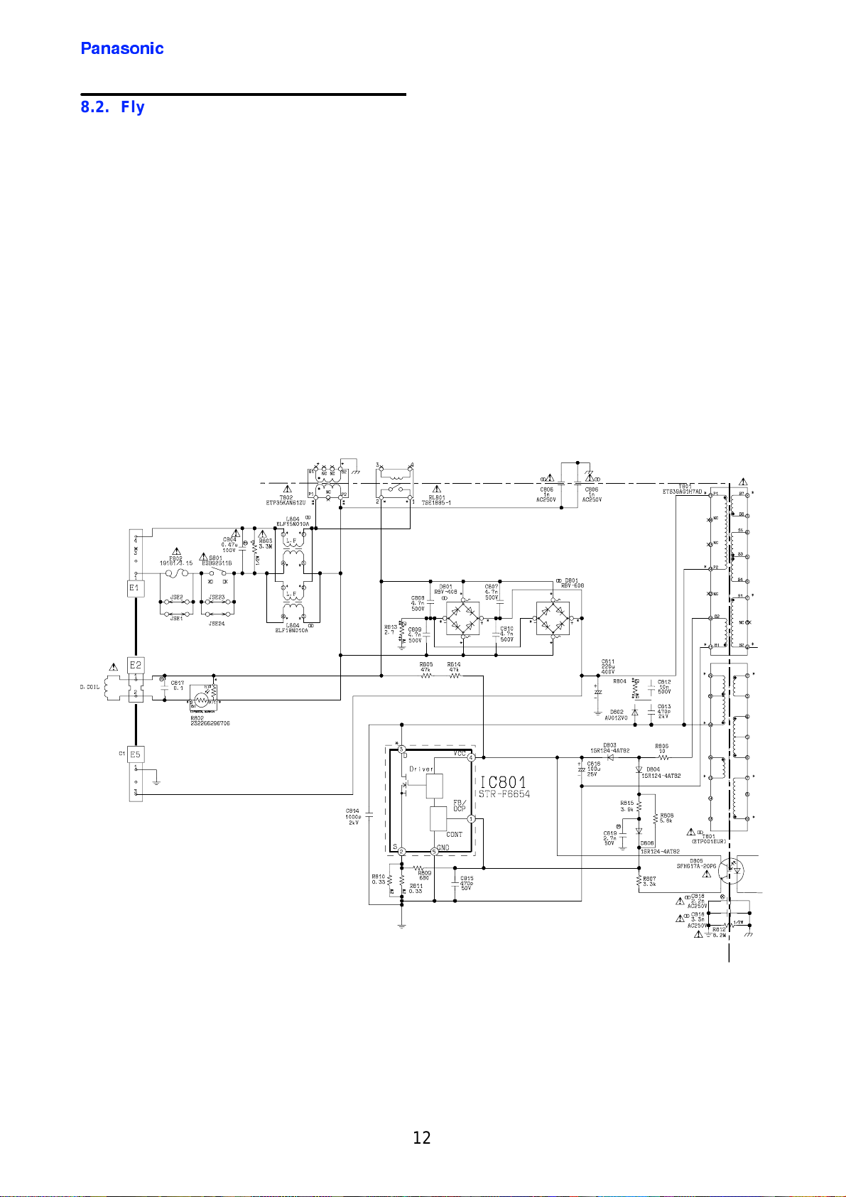
8. POWER SUPPLY
The supply voltage in the EURO 4 chassis is
provided by the integrated circuit STR-F6654.
As well as the main power supply a standby power
supply is also used. The benefits of which result in a
reduction in the power consumption when in standby
mode.
The mains A.C. voltage is input via connector E1
and fed to the standby transformer T802, via the
main TV ON/OFF switch S801.
At the standby transformer T802 the A.C. supply
splits into two paths.
The first path sees the A.C. supply being fed to the
normally open contact of the standby relay RL801.
The second path has the A.C. supply being fed via
the windings P1/P2 of the standby transformer
T802.
8.1. Standby Power Supply Circuit
The standby transformer T802 has the A.C. supply
as just mentioned being fed via the primary winding
P2/P1.
From the output of the secondary windings S2/S1 of
the standby transformer, a 5V standby supply is fed
via resistor R860, where the supply takes two paths.
1. The first path that the standby supply follows is
via capacitor C869 and rectifying diode D868,
this supply is then smoothed by capacitor C870.
This rectified andsmoothed supply is then again
split into two paths.
10

:
The first pathsees the supply voltage being
fed via resistor R861 to the standby relay
RL801 and therelay windingto the collector
oftransistor Q853. TransistorQ853 whichis
controlled by Q854, is responsible for
switching the TV into and out of standby
mode under the control of the
microprocessor IC, IC1101 pin 52.
When Q853 is switched ON current flows
through the winding of the relay and
collector / emitter junction of Q853. This
current flow causes the relay contact to
close feeding the mains supply to the bridge
rectifier and the switched mode power
supply IC IC801.
A 12V supply is also fed from the main
power supply via R863 and D871, this
supply beingused to reduce the load onthe
standby transformer when the TV is in
normal operation.
3DQDVRQLF
:
The second path is via resistor R862 to the
base of transistor Q852. This supply being
regulated by the zener diode D872 is used
as a base bias.
2. The second path from the standby transformer
T802, that the supply voltage follows is via the
rectifying diode D867 and smoothing capacitor
C871. Here the supply is applied to the collector
of Q852. From the emitter of Q852 a 5V standby
supply is fed to the Microprocessor IC1101,the
EPROM IC1102, the EAROM IC1103 and AV
Link circuit consisting of transistors Q1104 -
Q1107.
This supply allows these circuits to operate
during standby which is required to process the
switch ON command from the remote control or
local keys, allowing the TV to be switched out of
standby, or to also process AV Link commands.
11
3DQDVRQLF
8.2. Fly back Conv erter Powe r Supply
The STR-F6654 is a hybrid IC with built-in
MOS-FET and control IC as well as a separate
oscillation circuit.
It features a small SIP (Single In-line Package) with
isolated body (no bush and micra isolator required)
and requires only a small number of external
components.
Quasi-resonant operation is used to improve the
switching efficiency, which with altered operation in
standby mode allows the supply to fulfil both
power-on and standby roles.
The IC features pulse-by-pulse overcurrent
protection, over-voltage protection (with latch) and
thermal protection functions.
8.2.1. General
The mains voltage flows through the mains
suppression filter and standby relay, before being
fed via the bridge rectifier D801 and transformer
T801 primary windings P1/P2 to pin 3 of IC801 and
the drain terminal of the internal MOS-FET
transistor.
As there is no gate control voltage at this time the
operating voltage is not subjected to any load.
12

8.3. StartUp Circuitry
3DQDVRQLF
The start-up circuit is used to start and stop
operations of the control IC IC801, by detecting the
voltage appearing at the Vcc terminal, pin 4.
At start-up, capacitor C816 is charged via the
start-up circuit consisting of resistors R805, R814
which applies 16V to pin 4 of IC801.
The voltage applied to pin 4 of IC801 is then fed to
the start circuit, over-voltage monitor and latch
circuit which is used to control the oscillator and
drive stage. With pin 4 at 16V, IC801 begins to
operate and drive the internal MOS-FET transistor
into conduction resulting in current flow via the
primary winding, pin 3 (drain terminal) and pin 2
(source terminal) of IC801.
Once IC801 begins to operate the supply voltage at
pin 4 is supplied via the rectifying diode D803 and
smoothing capacitor C816 which is fed from the
drive winding of the switching transformer T801.
This supply voltage which is fed from the drive
winding B2 of T801 is initially unable to provide the
supply voltagedemanded and so the voltage at pin 4
decreases.
The charge held by C816 however slows this
decreasing voltage at pin 4 long enough to prevent
the shut down voltage of 10V being reached, thus
allowing the drive winding voltage at B2 to become
established.
13
3DQDVRQLF
8.4. Operation
When the internal MOS-FET transistor of IC801
conducts the current flows via the primary winding
P1 / P2 of T801 and IC801 pin 3 (Drain) and pin 2
(source) causing a voltage drop across R810, R811
to develop.
This voltage drop across R810, R811 is then fed
back to pin 1 of IC801 via a noise filter made up of
R809, C815.
This feedback voltage at pin 1 (approx. 2.5V) is then
fed to an internal comparator that is used to detect
when the voltage at pin 1 exceeds the internally
generated 0.73V reference signal. When this
condition is detected the internal MOS-FET
transistor is switched OFF.
At the same time once IC801 begins to operate Vcc
pin 4 is supplied from the drive winding B2/B1 as
mentioned previously.
This voltage developed in the drive winding is also
fed via an RC Network consisting of D804, R815,
C819 and D806 (located between the drive winding
of T801 and pin 1 of IC801) which is used to delay
the switch ON of the internal MOS-FET transistor,
allowing zero current switching. This reduces
switching losses that occur as a result of operating
with high switching frequencies.
When the internal MOS-FET transistor of IC801 is
switched OFF as described earlier the flow via the
primary winding P2, P1 stops. This results in the
collapse of the magnetic field and the energy stored
in the primary winding is transferred to the
secondary windings.
During this period the voltage at pin 1 of IC801
begins to fall at a rate determined by C819.
When the internal comparator of IC801 detects that
the voltage at pin 1 is below the internally generated
0.73V reference signal the MOS-FET is switched
ON and the cycle is repeated.
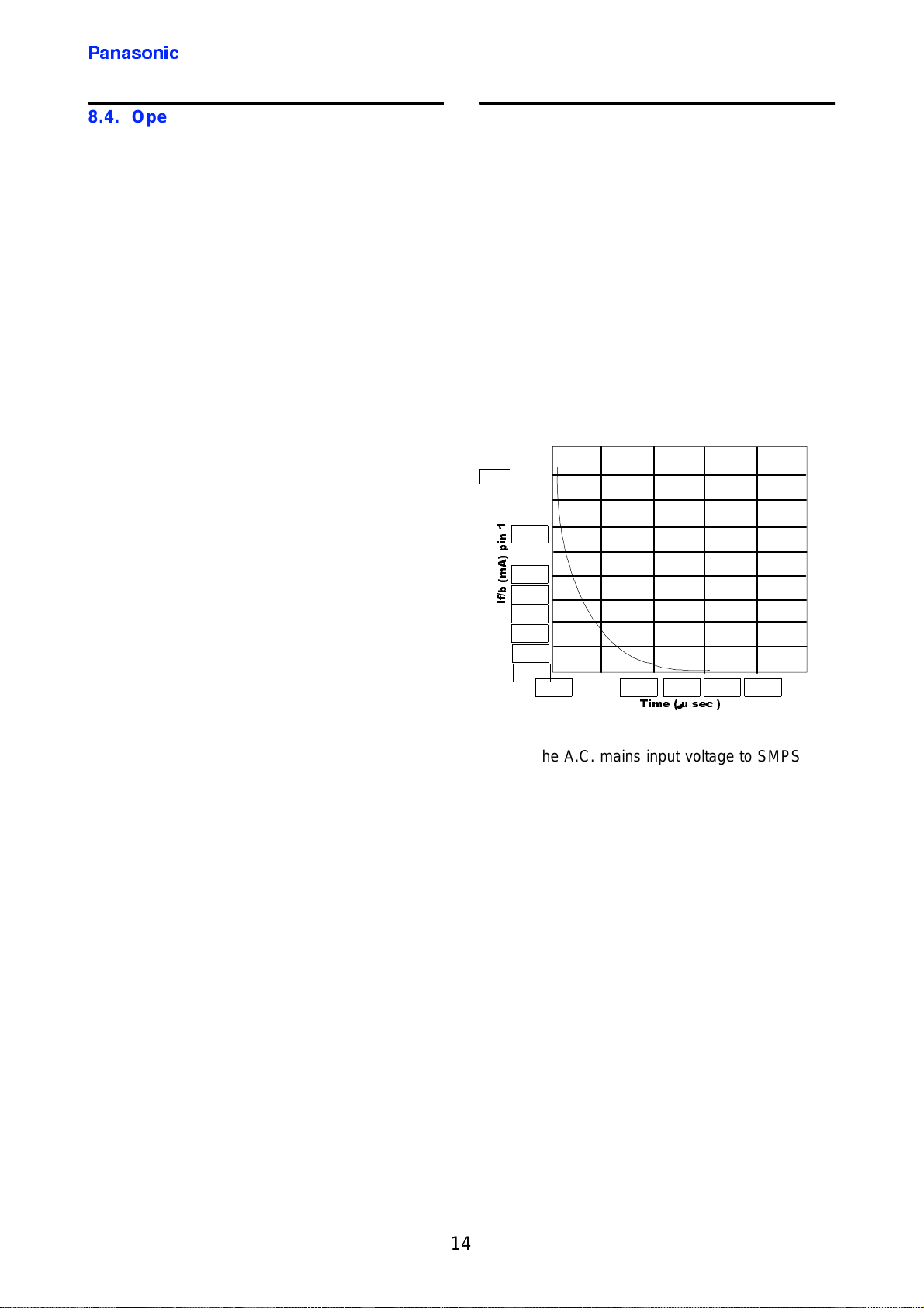
8.5. Regulation
The power supply ON time is controlled by
controlling the feedback supply to pin 1 of IC801.
This is achieved by the use of the photocoupler
D805.
The photocoupler current varies in response to the
level at pin 2 of the comparator IC IC850.
IC850 is used to monitor the 150V (B+) supply by
comparing the 150V secondary voltage with an
internally established reference voltage within
IC850.
The figure below shows how the ON time changes
against the current fed via D805 to pin 1 of IC801.
0.900
0.800
0.700
0.600
Q
L
S
0.500
$
0.400
P
E
I
0.300
,
0.200
0.100
0
01020 30 40 50
7LPHXVHF
If either the A.C. mains input voltage to SMPS gets
higher, or the load current on the secondary gets
smaller, pin 2 of IC850 reduces.
This causes the current flowing via the photocoupler
D805 to pin 1 of IC801 to increase, resulting in the
ON time of the internal MOS-FET transistor of IC801
to become shorter. This in turn causes the
secondary B+ level to return to its nominal value.
14
3DQDVRQLF
8.6. ProtectionCircuitry
8.6.1.Thermal Shut-down
This circuit triggers the latch circuit when the body of
the IC exceeds 140
8.6.2.Overvoltage Protection
The Overvoltage protection (OVP) is used to trigger
the latch circuit (mentioned later) when the Vcc
voltage at pin 4 exceeds 22V.
Although the OVP circuit basically functions as
protection of the Vcc terminal, it also prevents over
voltage at the secondary output, since the Vcc
terminal is supplied from the drive winding of
transformer T801, whose voltage is proportional to
its output voltage from the secondary windings.
8.6.3.Overcurrent
The Overcurrent protection (OCP) is performed
pulse-by-pulse by detecting the peak of the drain
current of the MOS-FET in every pulse and which is
used to reverse the internal oscillator output of
IC801.
The MOS-FET drain current is detected by inputting
the voltage drop developed across R810, R811 into
pin1ofIC801 via the noise filter circuit R809, C815.
When this input voltage exceeds the internally
generated reference signal of 0.73V the drive output
is pulled LOW, resulting in the internal MOS-FET of
IC801 switching OFF and the power supply
stopping.
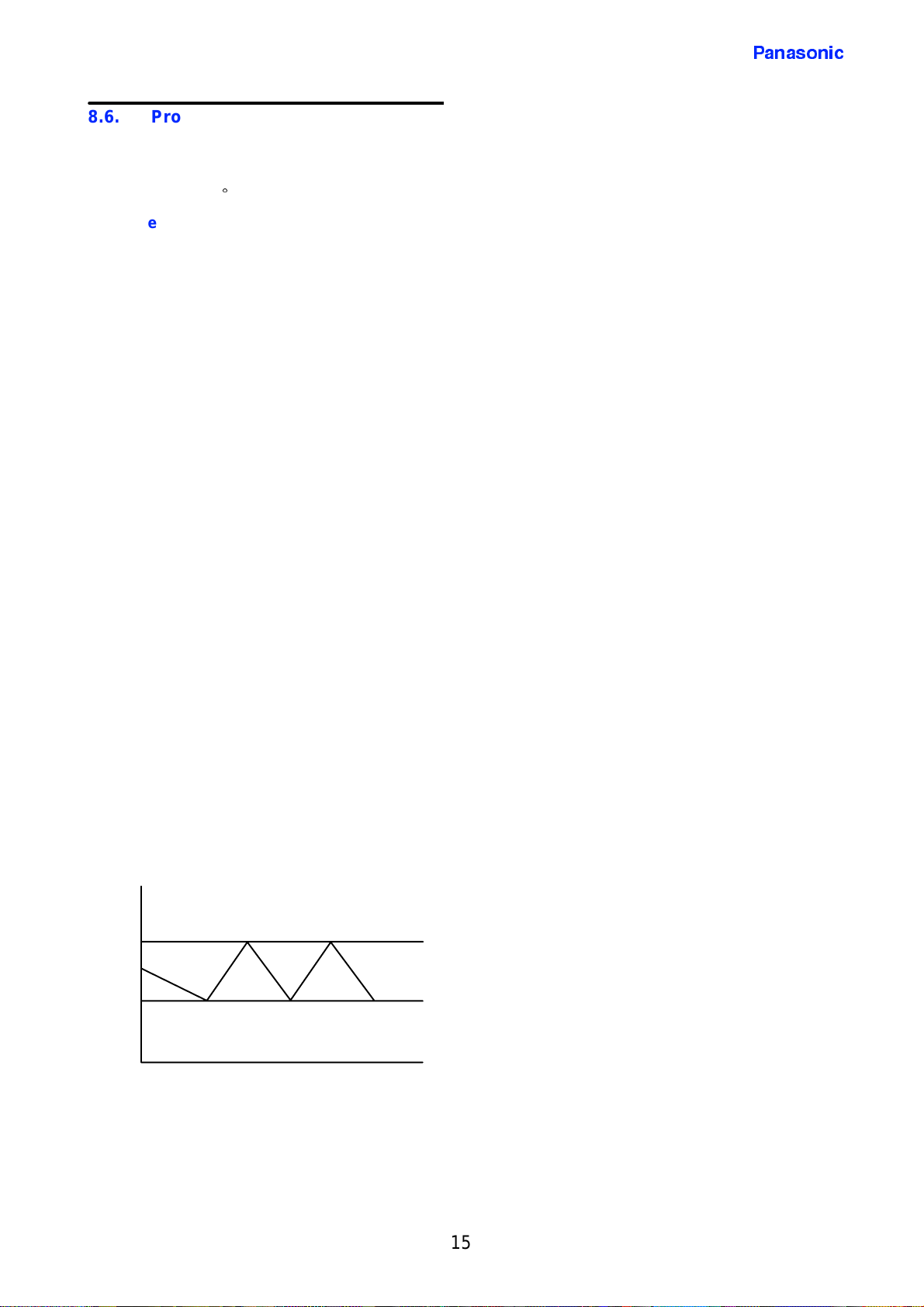
8.6.4.Latch
The latch circuit is used to keep the output from the
oscillator low stopping the power supply operating
when the overvoltage (OVP) and thermal shut-down
(TSD) circuits are in operation.
Vin
16V
(TYP)
10V
(TYP)
C
In this condition the Vcc input (pin 4) voltage
decreases until the the Vcc input reaches the
shut-down voltage of 10V . At this point pin 4 begins
to rise again but when it reaches the start up level
(16V) the latch circuit continues to stop the drive.
When the latch is ON, Vcc pin 4 voltage increases
and decreases within the 10V to 16V range, as
shown in the above fig. and is prevented from rising
normally.
Cancellation of the latch is achieved by switching
OFF the TV and disconnecting the AC input to the
circuit.
8.6.5.150V Line Protection
In-conjunction with the above mentioned protection
circuits, the 150V line is separately monitored for
over voltage protection (OVP) and over current
protection (OCP).
The OVP is monitored by zener diode D875, which
when its breakover voltage is exceeded causes
transistor Q855 to conduct. This results in the base
of Q853 being pulled LOW, causing Q853 to be
switched OFF.
When transistor Q853 is no longer conducting then
no current flow takes place via the standby relay
winding and the collector/emitter junction of
transistor Q853. The result of no current flow via the
standby relay winding causes the normally open
relay contact of the standby relay RL801 to open,
stopping the supply of the mains voltage to the
power supply circuit causing the TV to switch into
standby.
Likewise where an over current situation occurs then
an increased voltage drop across current limiting
resistor R877 develops. This increased voltage drop
biases on Q857 which feeds a HIGH level via the
emitter/collector junction of Q857 to the base of
Q855. When transistor Q855 conducts, Q853
becomes non-conducting resulting in the TV being
switched into standby mode.
15
3DQDVRQLF
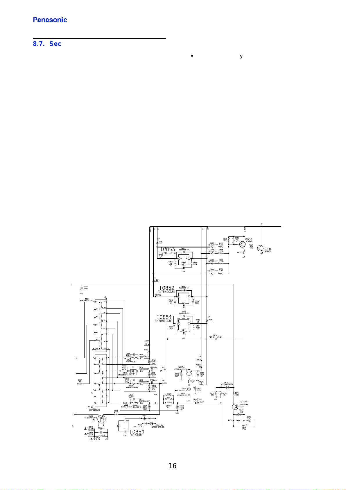
8.7. Se condary side
On the secondary side the transformer supplies the
following voltages :
1. 150V to supply the line output stage
2. 12V and 5V to supply an operating voltage to
the digital processing ICs.
3. 29V to supply the audio output stage
Although the secondary voltages are relatively
stable with short term load variations being
compensated for by IC801, it is still necessary to
stabilise the following voltages: 5V, 8V 9V (
Screen Models ONLY
The voltages which do not require further
stabilisation are :
150V supply for the line output stage ,
27V for the line driver stage
29V supply for the A.F. output stage
8.7.1.Voltage Stabilisation
The stabilisation of the previously mentioned
secondary supplies is performed as follows:
) and 12V.
Wide
:
A 15V supply which is fed from the
transformer T801 is fed to pin 1 of IC851
which is used to produce a stabilized 12V
supply. This supply is then also used to
produce the 9V (
) and 8V supplies.
ONLY
The wide screen models which use a 9V
supply is produced by feeding 12V to pin 1
ofIC852 whichthen outputs 9Vviapin3 and
which is used by the tuner/IF stage.
Likewise IC853 is also fed 12V to pin 1,
whichoutputs astabilised8V used tosupply
MSP IC2101.
The 5V supply is produced by feeding 7V to the
collector of series regulating transistor Q850 which
at its emitter outputs a 5V supply. The zener diode
D657 in the base of Q850 is used to maintain the
base of Q850 at a constant potential.
Wide Screen Models
16
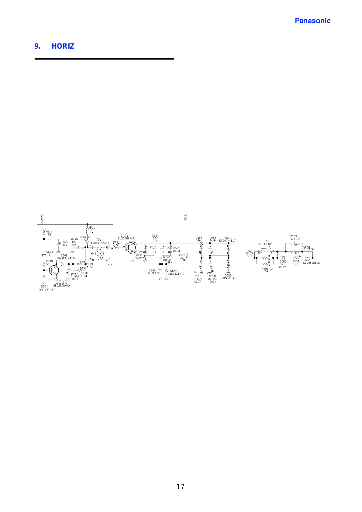
9. HORIZONTAL/VERTICAL OUTPUTS
3DQDVRQLF
9.1. Horizontal Driver
The line frequency control pulses for the horizontal
driver stage are output via pin 50 of the VDP IC601
at 1v pp and fed via C508 to the base of transistor
Q503.
Diode D501 permits rapid discharge of capacitor
C508 in the blocking phase of Q503.
From the circuitry of the line buffer stage, as well as
from the driver of the line output stage, it can be
clearly seen that this is low impedance current
control. The driver stage is fitted with a transistor
which is able to supply the necessary base control
current of up to 0.9 Amps for the driver transformer
T501 of the output stage.
To limit the inductive breaking peaks during the
blocking phase, the RC. combination R509, R510,
C51 1 are connected in parallel to the primary
winding of T501.
The driver stage operates in alternating mode in
relation to the output stage, i.e. when Q503 is
rendered conductive. Q551 is off and vice versa.
17

3DQDVRQLF
9.2. HorizontalOutputStage
Control of the horizontal output stage, or to be more
precise, the horizontal switching transistor, is
achieved as explained in the previous section.
Essentially, the base resistance of the horizontal
switching transistor consists of the very low
impedance resistor R506 and the series connected
secondary winding of driver transformer T501.
In practice, the parallel connected east/west
modulator diodes D551, D552 perceptibly reduce
the load on the switching transistor.
This type of transistor additionally possesses an
integrated diode section in p arallel to the
collector-emitter section which conducts in inverse
mode i.e. negative applied to the collector.
This inverse mode of the transistor takes place
during the first half of the sweep, up to about line
centre. In the subsequent second half of sweep, the
transistor operates in normal mode again with
conductive base emitter junction.
Only during the relatively brief flyback time is the
switching transistor blocked.
By virtue of the low impedance circuitry already
described, it is possible for base peak currents of
between + 0.9A and - 0.9 A to flow sufficiently
quickly in both directions.
It can be imagined that the significantly higher
emitter currents (i.e. max. = 4.5 A) cause enormous
"flooding" of charge carriers in the N-P and P-N
junctions of the semiconductor.
To ensure that the rapid switching action takes place
and that the charge carriers can discharge rapidly in
the base zone, base driving has been made
correspondingly low-impedance.
In connection with this, it should also be mentioned
that the control pulses have been formed specially
for dual utilisation of Q551 in normal and inverse
mode. In principle, the pulse duty factor of the base
drive has been altered from 12
52
m
S sweep time to 20mS flyback time and 44mS
sweep time. Thus, it is also possible to process any
unavoidable delays in the driver transformer. As a
result of prompt driving, the switching transistor has
adequate preparation for the subsequent operation
phase.
The supply voltage of the horizontal output stage is
taken from the switched mode power supply whichis
approximately 147v for CRT sizes of 66cm (28 ins)
and 59cm (25 ins). The exact control and switching
waveform during a line period corresponds to that of
the switched resonant circuit.
Here, the line switching transistor operates by virtue
of its three operating states. Conductive. Inversely
Conductive, and Off, in such a way that the charge
and discharge processes of collector capacitor C551
and inductor L552 produce the sweep and flyback
intervals exactly.
Only during the horizontal flyback time, is Q551
blocked for 20
parallel resonant circuit forms, (by virtue of its being
charged by the supply voltage), the positive half of a
sine wave oscillation.
The natural tendency of a parallel resonant circuit to
reverse the charge stored in the capacitor
subsequently into the inductor as magnetic energy,
leads to polarity reversal of the current.
From this, the negative component of the sine wave
oscillation normally forms at the collector of Q551.
This tendency is however prevented by the
Collector/Base diode section of Q551.Afterthe
collector/base start up voltage has been reached,
the transistor becomes conductive and clips the
negative component. The east/west modulator
diodes would also assist this function and thus
reduce the power dissipation in the switching
transistor.
m
S. The capacitor (C551) in the
m
S flyback time and
18
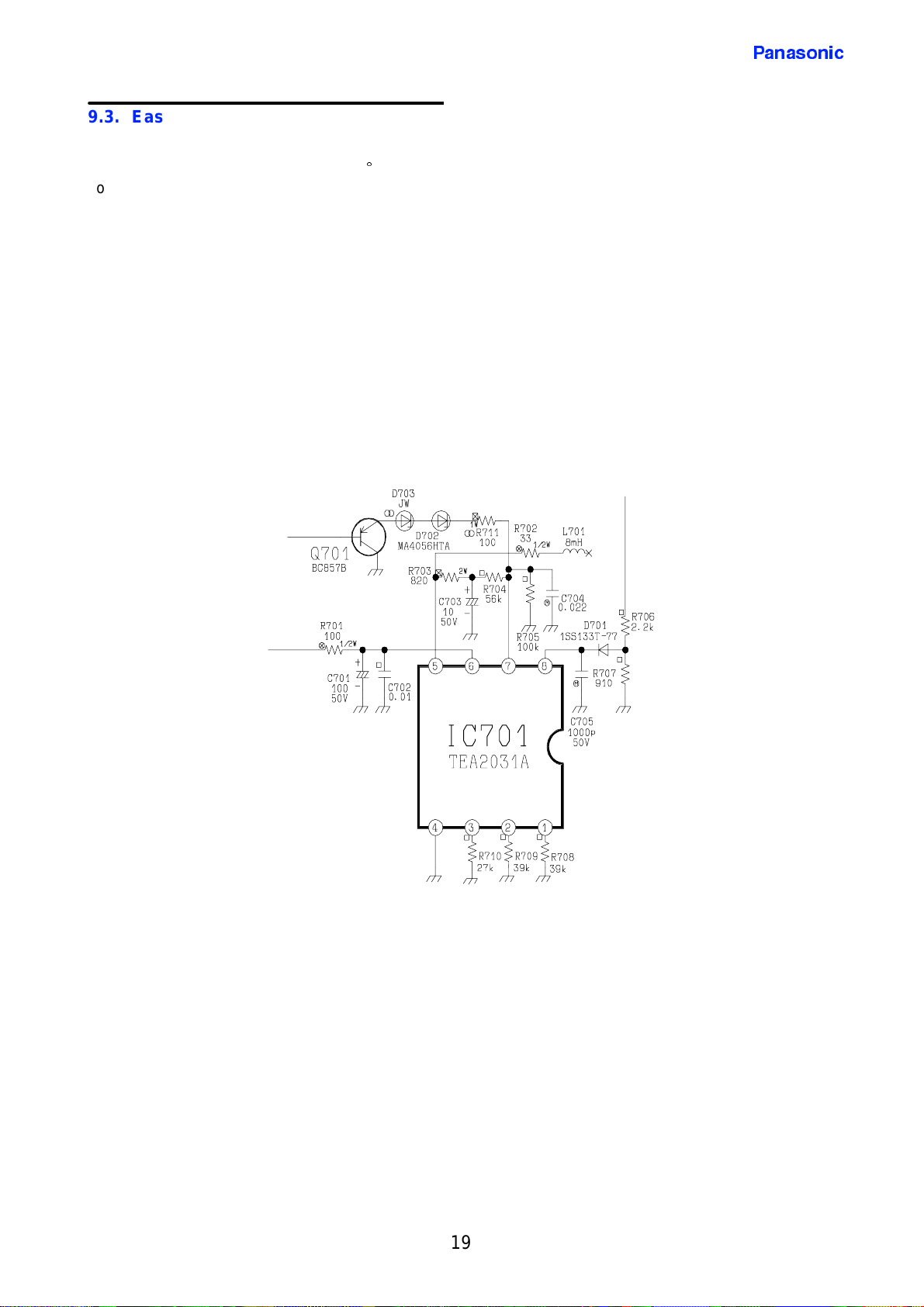
9.3. East/WestCorrection
3DQDVRQLF
To compensate for the pincushion distortion in
east/west direction in the case of 110
horizontal deflection current must be increased at
vertical centre in relation to vertical start and vertical
end.
This correction is achieved by the horizontal
deflection current being influenced with a vertical
frequency parabola in the east/west diode modulator
D551, D552.
Output from the VDP IC601, pin 32 a parabola
waveform of 1v pp occurs which is passed via R847
sets, the
to buffer transistor Q701 before being input via pin 7
of the East / West IC. IC701.
Here the parabola waveform is fed to a comparator,
where the parabola waveform is compared with the
horizontal flyback pulse, from the output of the
comparator the E/W drive signal is output via pin 5
and fed to the diode modulator via R702 and the
E/W charging coil L701.
This E/W signal is then superimposed onto the
deflection current with the aid of the diode
modulator, thus performing E/W correction.
19
3DQDVRQLF
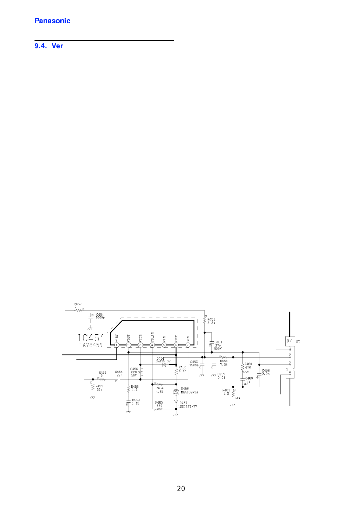
9.4. Vertical Output Stage
To drive the vertical output stage, the drive pulse is
output from the VDP IC601 pin 31 and fed to the
vertical output stage IC451 pin 5.
This vertical output IC IC451 consists of an
operational amplifier to which the vertical drive pulse
in the form of a sawtooth is passed, the results of
which are output via pin 2.
The gain of the internal op-amp. is controlled by the
negative feedback pulse which is fed via R454
connected between pin 2 and pin 5.
IC451 also contains a pump-up circuit which is used
to provide a switching voltage for the vertical flyback
period. This is required as the energy requirement of
the vertical output stage is highest during flyback, as
the electron beam has to be passed rapidly from the
bottom right hand corner of the screen to the top left
corner of the screen.
This brief additional energy requirement is met by
doubling the supply voltage available to the output
stage.
During vertical sweep, the bootstrap capacitor C456
is charged up to almost supply voltage via D454.
The output of the pump-up generator pin 7, IC451 is
at this moment at ground potential.
As a result of the DC displacement at the negative
pole of capacitor C456 (rising to the supply voltage),
build up of the supply voltage for the output stage at
pin 3 rises to almost twice the supply voltage. At the
same time, D454 is reverse biased and thus
prevents discharge of C456 into the supply line.
9.4.1.Vertical Protection
The output pin, pin 2 of IC451 which is directly
connected to the deflection coil is monitored by the
protection input of the VDP IC601.
Here a vertical flyback pulse is fed to pin 11 of the
VDP IC601, which is used to signal a fault (as
described in section 17.10.3. ).
When a fault is detected the RGB signals are
blanked preventing any damage of the CRT.
20
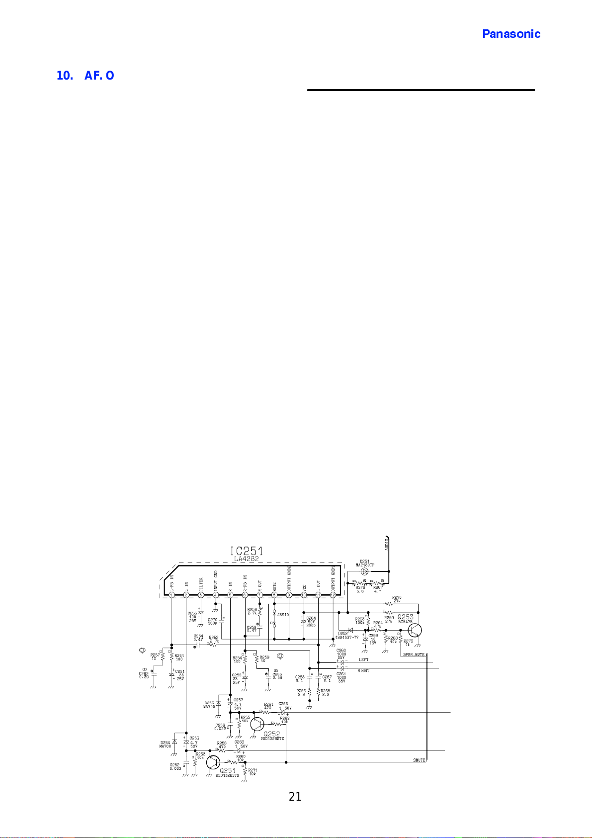
10. AF. OUTPUT STAGE
3DQDVRQLF
Both amplitude controlled AF signals are output from
pins 24 and 25 of IC2101 of the MSP.
The signals are fed to the base of transistors Q2102
and Q2103. The transistors are used for impedance
matching in order that the interference on the audio
lines between the MSP IC2101 and the audio output
I.C. IC251 is kept at a minimum.
The AF signals are fed to the audio output stage via
C266, R261 and C257 for the right hand signal and
C263, R256, C253 for the left. These capacitors may
be charged up very quickly as all control processes
(volume, balance) together with the base band
switch over are processed in the MSP IC2101.
Both AF signals are fed to pins 2 and 5 of the output
I.C. IC251. From here they are amplified and output
via pins 7 and 11. From here they are fed via the
headphone terminal to connectors E6 and E7 to the
internal speakers.
The usual negative feedback occurs from pin 11 to
pin 1 and from pin 7 to pin 6 of the I.C. via the R/C
network R252, C254 and R258 and C259. The
diodes at pins 2 and 5 D254 and D253 provide
protection for the output I.C. against any voltage
spikes by clamping the input pins. The output I.C. is
fed with a voltage of +29V to pin 10 of IC251.
10.1. Active Mute
The active mute circuit is used in parallel to the
inputs of the audio output IC IC251. This active mute
circuit consists of two transistors Q251 and Q252
which is controlled by transistor Q2101. Transistor
Q2101 is used to prevent POP during switch ON
and OFF times.
The POP mute circuit is fed a 5V supply and a12V
supply. The 5V supply which is fed via diode D2102
charges up capacitor C2129, while the 12V supply is
fed via R2113, charging up C2130. This 12V supply
is also fed to the emitter of transistor Q2101 via
D2103 this positive supply to the emitter causes
Q2101 to conduct, as its emitter is more positive
with respect to its base, as a results Q2101 feeds a
HIGH level to the base of transistors Q251 / Q252
forcing them into conduction and grounding the
audio lines preventing POP.
This mute line is held HIGH until C2130 has charged
up to a level where the base of Q2101 is no longer
negative with respect to its emitter and so Q2101
switches OFF, enabling the audio lines.
At switch OFF the 5V and 12V supply lines Fall
rapidly, resulting in C2130 discharging via D2104
into the falling 12V supply line. This causes Q2101
to conduct allowing the charge of C2129 to
discharge via the Emitter / collector junction of
Q2101 forcing the muting transistors Q251, Q252 to
conduct grounding the audio lines.
This POP mute control is also fed to transistors
Q2301, Q2303 whichare used to mute the audio fed
via the RCA monitor out terminal.
21

3DQDVRQLF
11. COLOUR OUTPUT STAGE
The Y-Board, contains not only the colour output
stage, but also scan velocity modulation (except
model TX-21MD4 which has no SVM stage).
The RGB signals fed to the colour output stage are
fed from the VDP IC601 pins 37 (R out),
38 (G out), 39 (B out), where these signals are fed
via the common base configured transistors Q301,
Q303 and Q305, which provided good high
frequency response, these signals are then buffered
and amplified by transistors Q302, Q304, Q306
before finally being fed via connectors E8 and Y2 of
the Y-Board. The RGB signals at this point being
approximately 5Vpp.
The velocity modulated (VM) signal which is a
combined RGB signal, is output from the VDP IC601
via pin 34 is also fed via a common base configured
transistor in the form of Q950, and from here via
Q951 where the signal again is amplified and
buffered before being fed to the Y-Board via
connectors E8, Y2 pin 7.
Transistors Q908 and Q909 then outputs the signal
at approximately 35Vpp, via connector Y6 pins 1
and 3 to the SVM coils, the scan coils being
controlled directly from the collector terminals of
transistors Q908 and Q909 via resistor R929 which
is coupled in parallel to the deflection winding.
11.2.CRT AMPLIFIER STAGE
11.2.1.Outline
In order to avoid damage caused by long cathode
lines and there by trim the frequency response, the
RGB output stage is mounted onto the CRT board.
Each of the 3 colour channels are fed to IC351
(TDA6103Q) which has a bandwidth of 7.5MHz
guaranteeing good resolution even with rapid signal
transitions in both directions.
The use of IC351 means that the number of
components in the colour output stage are reduced
to a minimum, the colour output stage being driven
directly by the VDP IC601.
11.1.Velocity Modulation circuit
The SVM signal which is fed via connector Y2 is
then fed to the base of transistor Q905 where with
capacitor C906 and R914 shape the signal.
The signal is then fed from here to two mirror image
push pull output stages which are used to supply the
required current to the velocity modulation coils.
Transistors Q906 and Q907 are connected as
impedance converters which control the output
stage at low impedance without distortion.
The RGB signals input to IC351 are amplified to
approximately 90Vpp before being output from
IC351 via their respective outputs with Red output
via pin 9, Green output via pin 8 and Blue output via
pin 7.
A reference voltage for the internal amplifiers is also
fed to IC351 pin 5, while negative feedback to
determine the amplification factor is provided by the
resistance between the input and output pins of the
RGB signals, this resistance being provided by
resistors R357, R358 and R359.
22
3DQDVRQLF
11.3.Tubeand PictureMeasurement
Tube and Picture measurements are carried out by
gating relevant information back via transistors
Q351, Q352 and Q353 to the sense input, pin 28 of
the VDP IC601. These Tube and Picture
measurements being discussed in detail in
section 17.9. of the VDP. However below is a brief
overview of Tube and Picture measurements.
11.3.1.Tube Measurement
%DVLFDOO\ WKH 7XEH PHDVXUHPHQW UHSUHVHQWV D
VDPSOLQJ FRQWURO FLUFXLW %\ HOHFWURQLF PHDQV LW
G\QDPLFDOO\ FRUUHFWV FRPSRQHQW WROHUDQFHV DQG DQ\
DJLQJ RI WKH &57 HWF
,Q DGGLWLRQ WKH IROORZLQJ DGYDQWDJHV DUH SURYLGHG
$XWRPDWLF EODFN OHYHO DQG ZKLWH OHYHO WUDFNLQJ
3UHYHQWLRQ RI FRORXU IDOVLILFDWLRQ GXULQJ WKH
SLFWXUH WXEH KHDWLQJ XS WLPH
,W KDV WKXV EHHQ SRVVLEOH WR GLVSHQVH ZLWK WKH
SUHYLRXVO\ FXVWRPDU\ EODFN OHYHO DQG ZKLWH OHYHO
FRQWUROV DQG WKH DGMXVWPHQWV LQYROYHG
11.3.2.Picture Measurement
'XULQJ 3LFWXUH 0HDVXUHPHQW ZKLFK LV FDUULHG RXW
GXULQJ DFWLYH SLFWXUH VFDQ PHDVXUHPHQW RI WKH
DFWLYH SLFWXUH PD[LPXP DQG PLQLPXP FXUUHQWV LV
FDUULHG RXW 7KLV LQIRUPDWLRQ EHLQJ XVHG WR SURYLGH
Beam Current protection
:
:
Artificial Intelligence (AI) function
This data then being input via the sense terminal
pin 28 of the VDP IC601.
11.4. ABL Regulation
This circuit which consists of Q552 and R564 is used
to keep the beam current at a constant level
avoiding degradation in Focus and at the same time
reducing blooming effects normally associated with
increases in beam current.
This circuit is arranged so that as the beam current
increases transistor Q552 switches OFF, this means
that resistor R564 is no longer in parallel with R262 /
R263 thus reducing the above mentioned artifacts.
%($0 &855(17 /,0,7$7,21
7KH PHDVXUHPHQW RI WKH EHDP FXUUHQW DV
PHQWLRQHG LQ WKH SUHYLRXV VHFWLRQ LV IHG YLD WKH
6HQVH LQSXW RI WKH 9'3 ,& SLQ WKH UHVXOW RI
WKH PHDVXUHPHQW EHLQJ FRPSDUHG WR WKH YDOXH
VWRUHG LQ PHPRU\ 7KH UHVXOW RI ZKLFK LV XVHG WR
UHGXFH WKH GULYH RI WKH EULJKWQHVV $' FRQYHUWHUV
DQG LI QHFHVVDU\ WKH FRQWUDVW $' FRQYHUWHUV
+RZHYHU LI WKH EHDP FXUUHQW IDLOV WR EH UHGXFHG WKH
WKH EHDP FXUUHQW VDIHW\ FLUFXLW LV XVHG WR VZLWFK RII
WKH 79
7KLV LV DFKLHYHG E\ WKH IO\EDFN WUDQVIRUPHU ZKLFK
ZRUNV ZLWK YLUWXDO HDUWKLQJ WKLV EDVLFDOO\ PHDQV WKDW
DV WKH EHDP FXUUHQW LQFUHDVHV WKH EDVH RI WKH
IO\EDFN WUDQVIRUPHU 7 EHFRPHV QHJDWLYH ,I WKH
EHDP FXUUHQW UHDFKHV WKH PD[LPXP FRQWURO UDQJH RI
WKH )%7 WKH ]HQHU GLRGH ' FRQGXFWV WKLV FDXVHV
SLQ RI WKH PLFURSURFHVVRU ,& WR JR /2:
UHVXOWLQJ LQ WKH 79 EHLQJ VZLWFKHG LQ WR VWDQGE\
UHIHU WR SDJH RI WKH PLFURSURFHVVRU VWDJH
11.6. S witch Off Spot Suppression
The switch-off afterglow flecks which would occur if
the CRTcharge was not reduced quickly enough are
suppressed by transistor Q354.
At switch-on and during operation Q354 has no
effect, since the base and emitter of Q354 are at the
same level and so non-conducting.
At switch-off Q354 isswitched ON bya rapidlyfalling
supply line. Diode D361 becomes reversed biased
preventing C363 from discharging into the supply
line. The capacitor C363 discharges via the
emitter/collector junction of Q354. This discharging
capacitor C363 is fed via diodes D362 / D363 / D364
which forces the colour output amplifiers of IC351
into saturation, discharging the CRT quickly and
preventing afterglow.
23
24
3DQDVRQLF

12. RF / IF SECTION
The EURO 4 chassis includes an RF/IF combi tuner
which is located on the E PCB. The RF stage of the
combi tuner being characterised by:-
(1) A high input impedance.
(2) Low radiation from tuner.
(3) Low oscillator interference.
The tuner is designed for reception not only of the
conventional frequencies to date, bands I, III, IV and
V and the intermediate special channel frequencies,
but also for the ’hyper’ band. This designation refers
to the frequency range from 300MHz to 470 MHz.
This frequency band is also of interest in view of the
growing number of cable networks and the
programmes which they offer.
A three band tuner is used for processing the large
frequency band from 47MHz to 681 MHz.
The extremely large tuning range in the bands
prohibits a band switch over with switching diodes
within the resonant circuits. Their switching capacity
in the VHF. band would:-
1. Excessively limit the tuning range.
2. Excessively limit the efficiency of the circuit
operation.
3DQDVRQLF
The IF stage of the combi tuner contains the video
and audio demodulators which are designed for the
most widely used TV standards. For this reason the
stage is referred to as the multi-standard IF stage.
The IF stage for the EURO 4 chassis comes in 2
versions as follows:
1. LA7577
This IC201 contained in the IF stage is used to
process both video and sound IF frequencies.
This IC IC201 LA7577 is used on models which
are not required to process the SECAM L
standard.
2. TDA9814
This IC201 contained inthe IFstage isalsoused
to process bothvideo andsound IF frequencies.
This IC IC201 TDA9814 being used on models
which are required to process the SECAM L
standards.
Once the video and sound IF signals have been
processed, the video signal is fed to the VDP IC601
and the audio signals to the MSP IC2101, all for
further processing.
Because of the above drawbacks each band has its
own bias stage, correction circuits and band filter
with optimised tuning diodes. Each "part tuner" can
thus be biased and set for its frequency range.
25
26
3DQDVRQLF
TV STANDARDS
13. MICROPROCESSOR AND TELETEXT PROCESSING
3DQDVRQLF
The microprocessor SDA5450 IC1 101 used on
EURO4, not only performs the required control
processing but also teletext processing which is
incorporated within the microprocessor, the
processing of which will be looked at later. First the
controlprocessing stage of the microprocessor willbe
looked at.
The elements that the microprocessor requires to
perform the aforementioned functions are:
:
8 bit C500-CPU
:
18MHz internal clock
:
Parallel 8-bit data and 16....19 bit address
bus
:
Eight 16 bit data pointer registers
:
Two 16 bit timers
:
Watch-dog timer
:
Capturecomparetimer forIRremote control
decoding
:
Serial Interface
6
%
9
&
)
(
/
/
/
,
,
,
5
)
)
)
,
:
256 bytes on-chip RAM
:
10kbytes on-chip display RAM
:
1 kbyte on-chip ACQ-buffer-RAM
:
1 kbyte on-chip extended-RAM
:
6 channel 8 bit pulse Width Modulator
:
2 channel 14 bit Pulse Width Modulator
:
4 multiplexed ADC inputs with 8 bit
resolution
:
One 8 bit In/Out port with open drain and
operational I
:
Two 8 bit multifunctional In/Out ports
:
One 4 bit port works as either digital or
2
C bus emulation
analogue input
:
One 2 bit In/Out port with optional functions
:
One 3 bit In/Out port with optional
RAM/ROM address expansion up to
512Kbyte
7
8
1
,
2
&
&
/
/
&
6
6
6
9
+
&DSWXUH
&RPSDUH
7LPHU
:DWFKGRJ
7LPHU
$'&
3:0
&38
3333
;
7
$
/
0DQDJHPHQW
;
5
7
'
$
/
:
5
77; 936
6OLFHU
0HPRU\
8QLW
008
3
$
3
'
6
(
1
$
/
(
$
3
$
77&
77'
([WHQGHG
'DWD
5$0
. %\WH
$FTXLVLWLRQ
'LVSOD\
&KDUDFWHU
520
7LPLQJ
'XDO3RUW
,QWHUIDFH
%XIIHU
'LVSOD\
*HQHUDWRU
'XDO3RUW
,QWHUIDFH
'LVSOD\
5$0
5
*
%
%ODQ
&RU
27
3DQDVRQLF
13.1. Microprocessor Stage
13.1.1.Input Control
:
Pins 3/4 - XIN / XOUT
Theinternaloscillator of theCPUissynchronisedwith
an external 6MHz quartz crystal X1101 which is
connected to pins 3 and 4.
TheClockfrequencies for theI
obtained from this frequency by internal dividing.
:
Pin 5 - Reset
During power On/Off operation, or during a fall in
voltage to the microprocessor IC1101, incorrect
operation may occur. To prevent this incorrect
operation the microprocessor IC1101 has a reset
signal input via pin 5. This reset signal is provided by
the reset IC IC1104 pin 1, which keeps the
microprocessor IC1101 in a stable condition until the
voltage level has risen and become stabilised.
ThisresetICIC1104whichisfed a 5Vstandbysupply
is input via pin 2.
At switch On this supply is less than 4.3V which
results in the reset IC IC1104 pulling pin 5 of the
microprocessor IC1101 Low, providing a stable
condition until the supply voltage becomes greater
than 4.3V. At this point the reset line goes High and
the microprocessor IC1101 begins to operate.
:
Pin 46 - HS
This input is used by the microprocessor for
synchronisation of the CVBS signal used for teletext
processing and display
:
Pin 47 - VS
This input is used by the microprocessor for
synchronisation of the CVBS signal used for teletext
processing and display.
:
Pin 54 - Reset In
This input terminal is used as a power OFF reset by
the microprocessor IC1101asthe TVis switchedinto
standby. Without this power OFF reset the
microprocessor IC1101 has no way of knowing the
operational condition of the TV.
When the TV is switched OFF the operational data
from the VDP IC601 and MSP IC2101 is lost, this
means that at switch ON the data has to bereloaded
back into the VDP IC601 and MSP IC2101.
Tobe able to do this the microprocessor IC1101,has
to be reset so that at switch ON from standby the
required operationaldata isreload back into the VDP
IC601 and MSP IC2101. This is achieved with reset
IC IC1105 which monitors the 5V supply line via pin
2.When the5V supply fallsto approximately4.3V the
2
Cbussystemarealso
reset IC IC1 105inputs a reset pulse via pin 54 of the
microprocessor IC1101.
:
Pin 58 - Slow1 / Pin 59 Slow2
The circuit is designed so that it is possible to switch
over to AV operation from all programme locations to
the desired AV interface. The AV inputs being:
1. AV1 21 pin scart socket allowing composite
video and RGB signal input . Slow switching
beingprovide via pin8for composite videoinput.
2. AV2 21 pin scart socket also allows composite
video input providing slow switching control via
pin 8. AV2 also allows the input for S-VHS input
as does AV3 (
The internal TV switching is performed by the VDP
IC601 is controlled by the microprocessor via I
Bus 1. By placing an AV turn on voltage at pin 8 of
the 21 pin AV sockets, the relevant A Vsocket will be
automatically selected. This turn on voltage fed from
AV1 and AV2 pin 8 is fed to IC1101 and the pins 58
(AV1) and 59 (AV2) microprocessor.
Pin 8 of AV1 and AV2 scart sockets are also used to
allow IC1101 of the microprocessor to perform
automatic picture ratio selection between 4:3 and
16:9 formats during AV operation.
However, a pre-requirement for this would be for
example, the provision of a video recorder able to
process both picture formats. It has been
established that during play-back recorders with a
picture format of 4:3 supply an AV turn on voltage of
12V, and those with an aspect ratio of 16:9 show a
turn on voltage of 6V. These switching voltages fed
from pin 8 of the 21 pin AV sockets and fed to the
microprocessor pins 58 (AV1) and 59 (AV2) are fed
via the potential divider resistors R1131, R1128, and
final R1 127 to pin 59 for AV2 selection. AV1
selection is fed via resistors R1130, R1129 and
R1 126 to pin 58 of the microprocessor IC1101.
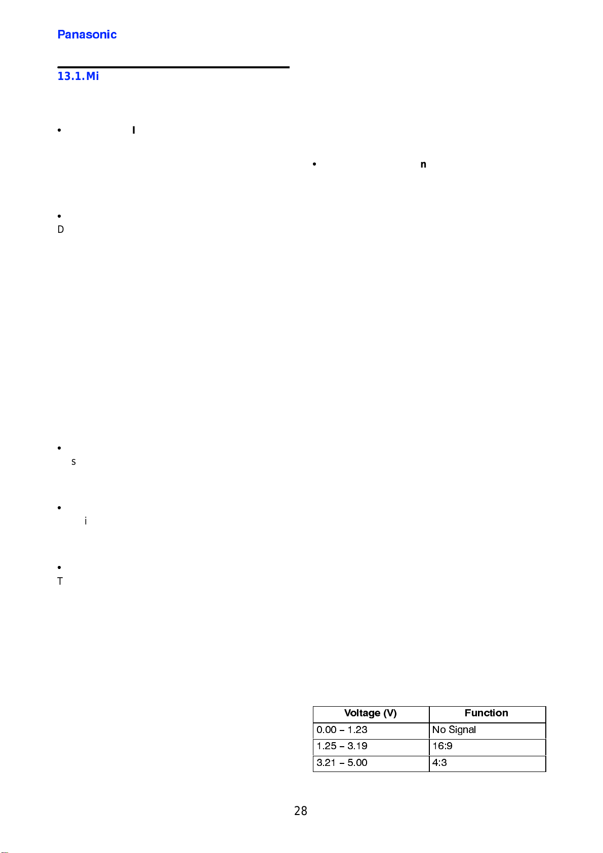
The table shown below shows the required voltages
for aspect ratio selection.
9ROWDJH 9 )XQFWLRQ
1R 6LJQDO
wide screen models only
)
2
C
28

:
Pin 60 - Keyscan
The local control commands are fed to the
microprocessor IC1101 as serial data. This data is
input via pin 60. This pin is held at 5V due to the
pull-up resistor R1161 which is connected to the 5V
standbysupply.Thismeans that thisHighlevelisalso
maintained during standby condition. Operating
commands fed from the local keys results in varying
voltages beingapplied to pin 60 which inturn initiates
the varies controls.
Operating commands issued from the local and
remote control are treated with equal status,
:
Pin 61 - AFC
During search mode the microprocessor IC1 101
detects the AFC voltageinput via pin 61, whichis fed
from the tuner/I.F. stage.
WhentheAFCvoltagereaches midlevelbetweenthe
highest and lowest points of its swing, the
microprocessor stopsthesearch operation and holds
the data.
3DQDVRQLF
:
Pin 68 - CVBS In
This composite video signal which is input via
pin 68 is used for teletext processing which is carried
out within the microprocessor IC1101.
:
Pin 71 - VProt
This input is used to detect a fault in the deflection
circuit. Where there are no errors a HIGH level is
applied to the base of Q451 which results in this
transistor beingin theOFF state. When Q451 isOFF
a HIGH level is applied to pin 71 of the
microprocessor IC1101 which is fed via resistor
R457, this HIGH level ensuring the microprocessor
IC1101 is inoperative.
Where an error occurs a LOW level is applied to the
base of transistor Q451 causing the transistor to
conduct. When transistorQ451 conducts pin71ofthe
microprocessor IC1101 is pulled LOW, this results in
theTVbeingswitchedinto standby after a short delay.
:
Pin 63 - 65 - FLT1-3
FLT3pin 63 is used for the phase shifting of the VPS
or teletext data.
FLT2 pin 64 PLL filter for VPS slicing.
FLT1 pin 65 PLL filter is used by the teletext slicer.
:
Pin 67 - IRef
This is a reference current for internal PLL.
:
Pin 74 - RC
The users commands for control of the TV receiver
are applied via the remote control.
Thesecommands from theremotecontrol transmitter
are applied via RPM-637CBRL IC1061 (
remote controlreceiver andQ1051 (
of IC1101, this command data being in serial format.
IC1071
Q1061
)the
) to pin74
29
3DQDVRQLF
:
Pin 75 - Prot1
The microprocessor IC1101 pin 75 which is normally
heldHighvia R1149providesa protection input which
is used to switch the TV into standby mode. The
protection input has two hard wired protection
circuits, these being:
:
ABL protection
During normal operation the beam current is
measured, with the result being input via the sense
input of VDP IC601, pin 28.
As already mentioned the beam current limitation is
carried out via software control, the results of this
being used to back off the RGB output amplifiers in
this I.C. to a greater or lesser extent, thereby limiting
the beam current.
Where the control limit is exceeded, although the
amplifiers have been completely reversed (which
may leadto an error in the RGB finaloutputs or there
voltage supply), defects in the CRT may result if no
protective measures are taken.
,Q RUGHU WR DYRLG WKLV ]HQHU GLRGH ' LV
LQFRUSRUDWHG LQWR WKH FLUFXLW
'XULQJ QRUPDO RSHUDWLRQ WKH ]HQHU GLRGH ' LV
QRQFRQGXFWLQJ DQG 3LQ RI WKH PLFURSURFHVVRU
,& LV KHOG +LJK YLD UHVLVWRU 5 ,Q WKLV VWDWH
WKH SURWHFWLRQ FLUFXLW GRHV QRW RSHUDWH
:KHUH DQ HUURU GHVFULEHG DULVHV DQG WKH EHDP
FXUUHQW FRQWLQXHV WR ULVH WKHQ WKH ]HQHU GLRGH '
FRQGXFWV GXH WR WKH QHJDWLYH YROWDJH IHG EDFN IURP
7 )O\EDFN WUDQVIRUPHU ZKLFK FDXVHV GLRGH
' WR FRQGXFW SXOOLQJ WKH DQRGH RI WKH ]HQHU GLRGH
' ORZHU WKDQ LWV FDWKRGH $V LWV DQRGH LV SXOOHG
ORZHU LWV FDWKRGH EHFRPHV PRUH SRVLWLYH 2QFH WKH
]HQHU GLRGHV EUHDNRYHU YROWDJH LV UHDFKHG SLQ RI
PLFURSURFHVVRU
:KHUH XSRQ DIWHU D VKRUW GHOD\ WKH PLFURSURFHVVRU
IC1101
The Voltage supply lines are monitored for short
circuit faults,the supply lines monitored are:
If a fault occurs resulting in one of the
aforementioned supplies failing then the safety
diode connected to that supply will conduct. This will
result in the base of Q851 (which is switched OFF
during no fault conditions) going low with respect to
its emitter. In this condition Q851 would conduct
biasing ON Q856, this would cause pin 75 of the
microprocessor IC1101 to go LOW and the TV
would shut down into standby.
VZLWFKHV WKH 79 LQWR VWDQGE\
:
Voltage supply lines protection
:
12V supply monitored via D863
9V supply monitored via D864
(
8V supply monitored via D865
5V supply monitored via D866
IC1101
wide screen only
LV SXOOHG /2:
)
30
 Loading...