

Panasonic PAN1322-SPP, ENW89841A3KF User Manual

August 2013
ENW89841A3KF
Bluetooth QD ID:B021246 (End Product Listing)
FCC ID: T7VEBMU
IC ID: 216QEBMU
PAN1322-SPP
Intel’s
BlueMoonUniversal Platform
Wireless Modules
User’s Manual
Hardware Description
Revision 1.3

Edition 2013-08-14
Published by
Panasonic Industrial Devices Europe GmbH
Zeppelinstrasse 19
D-21337 Lüneburg, Germany
© 2013 Panasonic Industrial Devices Europe GmbH
All Rights Reserved.
Legal Disclaimer
The information given in this document shall in no event be regarded as a guarantee of conditions or
characteristics. With respect to any examples or hints given herein, any typical values stated herein and/or any
information regarding the application of the device, Panasonic Industrial Devices Europe GmbH hereby disclaims
any and all warranties and liabilities of any kind, including without limitation, warranties of non-infringement of
intellectual property rights of any third party.
Information
For further information on technology, delivery terms and conditions and prices please contact your nearest
Panasonic Office in Germany or one of our Distributor or write an e-mail to wireless@eu.panasonic.com.
Warnings
Due to technical requirements components may contain dangerous substances. For information on the types in
question please contact your nearest Panasonic Office.
Panasonic Electronic Devices may only be used in life-support devices or systems with the express written
approval of Panasonic Devices, if a failure of such components can reasonably be expected to cause the failure
of that life-support device or system, or to affect the safety or effectiveness of that device or system. Life support
devices or systems are intended to be implanted in the human body, or to support and/or maintain and sustain
and/or protect human life. If they fail, it is reasonable to assume that the health of the user or other persons may
be endangered.

ENW89841A3KF - Intel’s BlueMoonTM Universal Platform
Revision History: 2013-08-14, Revision 1.3
Previous Version: 1.2
Revision Subjects (major changes since last revision)
Rev1.0
Rev1.1
Rev1.2
Rev1.3
Trademark Information:
BlueMoon® is a trademark of Intel Mobile Communications GmbH.
IPhone®, iPad®, iPad® and Apple® are trademarks of Apple Inc.
Initial Version from 2013-02-01
Delete chapter 4.3, Update module picture on page 8, delete antenna reference list in chapter 9.1,
update chapter 9.8
Refer in chapter 1.7 FW Version to Appendix [2]
Update QD ID
PAN1322-SPP
ENW89841A3KF
User’s Manual 3 Revision 1.3, 2013-08-14
Hardware Description

PAN1322-SPP
ENW89841A3KF
Table of Contents
Table of Contents
Table of Contents . . . . . . . . . . . . . . . . . . . . . . . . . . . . . . . . . . . . . . . . . . . . . . . . . . . . . . . . . . . . . . . . 4
List of Figures . . . . . . . . . . . . . . . . . . . . . . . . . . . . . . . . . . . . . . . . . . . . . . . . . . . . . . . . . . . . . . . . . . . 6
List of Tables . . . . . . . . . . . . . . . . . . . . . . . . . . . . . . . . . . . . . . . . . . . . . . . . . . . . . . . . . . . . . . . . . . . . 7
1 General Device Overview . . . . . . . . . . . . . . . . . . . . . . . . . . . . . . . . . . . . . . . . . . . . . . . . . . . . . . . . . . 8
1.1 Features . . . . . . . . . . . . . . . . . . . . . . . . . . . . . . . . . . . . . . . . . . . . . . . . . . . . . . . . . . . . . . . . . . . . . . . . 8
1.2 Block Diagram . . . . . . . . . . . . . . . . . . . . . . . . . . . . . . . . . . . . . . . . . . . . . . . . . . . . . . . . . . . . . . . . . . . 9
1.3 Pin Configuration LGA . . . . . . . . . . . . . . . . . . . . . . . . . . . . . . . . . . . . . . . . . . . . . . . . . . . . . . . . . . . . . 9
1.4 Pin Description . . . . . . . . . . . . . . . . . . . . . . . . . . . . . . . . . . . . . . . . . . . . . . . . . . . . . . . . . . . . . . . . . . 10
1.5 System Integration . . . . . . . . . . . . . . . . . . . . . . . . . . . . . . . . . . . . . . . . . . . . . . . . . . . . . . . . . . . . . . . 13
1.6 SW Patch in EEPROM . . . . . . . . . . . . . . . . . . . . . . . . . . . . . . . . . . . . . . . . . . . . . . . . . . . . . . . . . . . . 14
1.7 FW Version . . . . . . . . . . . . . . . . . . . . . . . . . . . . . . . . . . . . . . . . . . . . . . . . . . . . . . . . . . . . . . . . . . . . . 14
2 Basic Operating Information . . . . . . . . . . . . . . . . . . . . . . . . . . . . . . . . . . . . . . . . . . . . . . . . . . . . . . 15
2.1 Power Supply . . . . . . . . . . . . . . . . . . . . . . . . . . . . . . . . . . . . . . . . . . . . . . . . . . . . . . . . . . . . . . . . . . . 15
2.2 Clocking . . . . . . . . . . . . . . . . . . . . . . . . . . . . . . . . . . . . . . . . . . . . . . . . . . . . . . . . . . . . . . . . . . . . . . . 15
2.3 Low Power Modes . . . . . . . . . . . . . . . . . . . . . . . . . . . . . . . . . . . . . . . . . . . . . . . . . . . . . . . . . . . . . . . 15
2.3.1 Low Power Mode . . . . . . . . . . . . . . . . . . . . . . . . . . . . . . . . . . . . . . . . . . . . . . . . . . . . . . . . . . . . . . . 15
2.3.2 Complete Power Down . . . . . . . . . . . . . . . . . . . . . . . . . . . . . . . . . . . . . . . . . . . . . . . . . . . . . . . . . . 15
2.3.3 ON/OFF . . . . . . . . . . . . . . . . . . . . . . . . . . . . . . . . . . . . . . . . . . . . . . . . . . . . . . . . . . . . . . . . . . . . . . 15
3 PAN1322-SPP Interfaces . . . . . . . . . . . . . . . . . . . . . . . . . . . . . . . . . . . . . . . . . . . . . . . . . . . . . . . . . 16
3.1 UART Interface . . . . . . . . . . . . . . . . . . . . . . . . . . . . . . . . . . . . . . . . . . . . . . . . . . . . . . . . . . . . . . . . . . 16
3.1.1 UART . . . . . . . . . . . . . . . . . . . . . . . . . . . . . . . . . . . . . . . . . . . . . . . . . . . . . . . . . . . . . . . . . . . . . . . . 16
3.1.1.1 Baud Rates . . . . . . . . . . . . . . . . . . . . . . . . . . . . . . . . . . . . . . . . . . . . . . . . . . . . . . . . . . . . . . . . . 16
3.1.1.2 Detailed UART Behavior . . . . . . . . . . . . . . . . . . . . . . . . . . . . . . . . . . . . . . . . . . . . . . . . . . . . . . . 17
3.1.1.3 UARTCTS Response Time . . . . . . . . . . . . . . . . . . . . . . . . . . . . . . . . . . . . . . . . . . . . . . . . . . . . . 17
3.2 Low Power Control . . . . . . . . . . . . . . . . . . . . . . . . . . . . . . . . . . . . . . . . . . . . . . . . . . . . . . . . . . . . . . . 17
4 General Device Capabilities . . . . . . . . . . . . . . . . . . . . . . . . . . . . . . . . . . . . . . . . . . . . . . . . . . . . . . . 18
4.1 RF Test Application . . . . . . . . . . . . . . . . . . . . . . . . . . . . . . . . . . . . . . . . . . . . . . . . . . . . . . . . . . . . . . 18
4.2 Firmware ROM Patching . . . . . . . . . . . . . . . . . . . . . . . . . . . . . . . . . . . . . . . . . . . . . . . . . . . . . . . . . . 18
4.2.1 Patch Support . . . . . . . . . . . . . . . . . . . . . . . . . . . . . . . . . . . . . . . . . . . . . . . . . . . . . . . . . . . . . . . . . 18
5 Ordering Information . . . . . . . . . . . . . . . . . . . . . . . . . . . . . . . . . . . . . . . . . . . . . . . . . . . . . . . . . . . . 18
6 Bluetooth Capabilities . . . . . . . . . . . . . . . . . . . . . . . . . . . . . . . . . . . . . . . . . . . . . . . . . . . . . . . . . . . 19
6.1 Supported Features . . . . . . . . . . . . . . . . . . . . . . . . . . . . . . . . . . . . . . . . . . . . . . . . . . . . . . . . . . . . . . 19
6.2 PAN1322-SPP Bluetooth Features . . . . . . . . . . . . . . . . . . . . . . . . . . . . . . . . . . . . . . . . . . . . . . . . . . . 19
6.2.1 Secure Simple Pairing . . . . . . . . . . . . . . . . . . . . . . . . . . . . . . . . . . . . . . . . . . . . . . . . . . . . . . . . . . . 19
6.2.2 Role Switch . . . . . . . . . . . . . . . . . . . . . . . . . . . . . . . . . . . . . . . . . . . . . . . . . . . . . . . . . . . . . . . . . . . 19
6.2.3 Sniff Mode . . . . . . . . . . . . . . . . . . . . . . . . . . . . . . . . . . . . . . . . . . . . . . . . . . . . . . . . . . . . . . . . . . . . 19
6.2.4 Sniff Subrating . . . . . . . . . . . . . . . . . . . . . . . . . . . . . . . . . . . . . . . . . . . . . . . . . . . . . . . . . . . . . . . . . 19
6.2.5 Enhanced Power Control . . . . . . . . . . . . . . . . . . . . . . . . . . . . . . . . . . . . . . . . . . . . . . . . . . . . . . . . . 19
6.2.6 Encryption Pause and Resume . . . . . . . . . . . . . . . . . . . . . . . . . . . . . . . . . . . . . . . . . . . . . . . . . . . . 20
7 Electrical Characteristics . . . . . . . . . . . . . . . . . . . . . . . . . . . . . . . . . . . . . . . . . . . . . . . . . . . . . . . . . 21
7.1 Absolute Maximum Ratings . . . . . . . . . . . . . . . . . . . . . . . . . . . . . . . . . . . . . . . . . . . . . . . . . . . . . . . . 21
7.2 Operating Conditions . . . . . . . . . . . . . . . . . . . . . . . . . . . . . . . . . . . . . . . . . . . . . . . . . . . . . . . . . . . . . 21
7.3 DC Characteristics . . . . . . . . . . . . . . . . . . . . . . . . . . . . . . . . . . . . . . . . . . . . . . . . . . . . . . . . . . . . . . . 22
7.3.1 Pad Driver and Input Stages . . . . . . . . . . . . . . . . . . . . . . . . . . . . . . . . . . . . . . . . . . . . . . . . . . . . . . 22
7.3.2 Pull-ups and Pull-downs . . . . . . . . . . . . . . . . . . . . . . . . . . . . . . . . . . . . . . . . . . . . . . . . . . . . . . . . . 24
User’s Manual 4 Revision 1.3, 2013-08-14
Hardware Description

PAN1322-SPP
7.3.3 Protection Circuits . . . . . . . . . . . . . . . . . . . . . . . . . . . . . . . . . . . . . . . . . . . . . . . . . . . . . . . . . . . . . . 24
7.3.4 System Power Consumption . . . . . . . . . . . . . . . . . . . . . . . . . . . . . . . . . . . . . . . . . . . . . . . . . . . . . . 25
7.4 RF Part . . . . . . . . . . . . . . . . . . . . . . . . . . . . . . . . . . . . . . . . . . . . . . . . . . . . . . . . . . . . . . . . . . . . . . . . 25
7.4.1 Characteristics RF Part . . . . . . . . . . . . . . . . . . . . . . . . . . . . . . . . . . . . . . . . . . . . . . . . . . . . . . . . . . 25
7.4.1.1 Bluetooth Related Specifications . . . . . . . . . . . . . . . . . . . . . . . . . . . . . . . . . . . . . . . . . . . . . . . . . 25
8 Package Information . . . . . . . . . . . . . . . . . . . . . . . . . . . . . . . . . . . . . . . . . . . . . . . . . . . . . . . . . . . . 29
8.1 Package Marking . . . . . . . . . . . . . . . . . . . . . . . . . . . . . . . . . . . . . . . . . . . . . . . . . . . . . . . . . . . . . . . . 29
8.2 Production Package . . . . . . . . . . . . . . . . . . . . . . . . . . . . . . . . . . . . . . . . . . . . . . . . . . . . . . . . . . . . . . 29
8.2.1 Pin Mark . . . . . . . . . . . . . . . . . . . . . . . . . . . . . . . . . . . . . . . . . . . . . . . . . . . . . . . . . . . . . . . . . . . . . . 30
9 Bluetooth Qualification and Regulatory Certification . . . . . . . . . . . . . . . . . . . . . . . . . . . . . . . . . . 31
9.1 Reference Design . . . . . . . . . . . . . . . . . . . . . . . . . . . . . . . . . . . . . . . . . . . . . . . . . . . . . . . . . . . . . . . . 31
9.2 FCC Class B Digital Devices Regulatory Notice . . . . . . . . . . . . . . . . . . . . . . . . . . . . . . . . . . . . . . . . . 32
9.3 FCC Wireless Notice . . . . . . . . . . . . . . . . . . . . . . . . . . . . . . . . . . . . . . . . . . . . . . . . . . . . . . . . . . . . . 32
9.4 FCC Interference Statement . . . . . . . . . . . . . . . . . . . . . . . . . . . . . . . . . . . . . . . . . . . . . . . . . . . . . . . . 33
9.5 FCC Identifier . . . . . . . . . . . . . . . . . . . . . . . . . . . . . . . . . . . . . . . . . . . . . . . . . . . . . . . . . . . . . . . . . . . 34
9.6 European R&TTE Declaration of Conformity . . . . . . . . . . . . . . . . . . . . . . . . . . . . . . . . . . . . . . . . . . . 34
9.7 Bluetooth Qualified Design ID . . . . . . . . . . . . . . . . . . . . . . . . . . . . . . . . . . . . . . . . . . . . . . . . . . . . . . . 36
9.8 Industry Canada Certification . . . . . . . . . . . . . . . . . . . . . . . . . . . . . . . . . . . . . . . . . . . . . . . . . . . . . . . 36
9.9 Label Design of the Host Product . . . . . . . . . . . . . . . . . . . . . . . . . . . . . . . . . . . . . . . . . . . . . . . . . . . . 36
9.10 Regulatory Test House . . . . . . . . . . . . . . . . . . . . . . . . . . . . . . . . . . . . . . . . . . . . . . . . . . . . . . . . . . . . 36
ENW89841A3KF
Table of Contents
10 Assembly Guidelines . . . . . . . . . . . . . . . . . . . . . . . . . . . . . . . . . . . . . . . . . . . . . . . . . . . . . . . . . . . . 37
10.1 General Description of the Module . . . . . . . . . . . . . . . . . . . . . . . . . . . . . . . . . . . . . . . . . . . . . . . . . . . 37
10.2 Printed Circuit Board Design . . . . . . . . . . . . . . . . . . . . . . . . . . . . . . . . . . . . . . . . . . . . . . . . . . . . . . . 37
10.3 Solder Paste Printing . . . . . . . . . . . . . . . . . . . . . . . . . . . . . . . . . . . . . . . . . . . . . . . . . . . . . . . . . . . . . 39
10.4 Assembly . . . . . . . . . . . . . . . . . . . . . . . . . . . . . . . . . . . . . . . . . . . . . . . . . . . . . . . . . . . . . . . . . . . . . . 39
10.4.1 Component Placement . . . . . . . . . . . . . . . . . . . . . . . . . . . . . . . . . . . . . . . . . . . . . . . . . . . . . . . . . . 39
10.4.2 Pin Mark . . . . . . . . . . . . . . . . . . . . . . . . . . . . . . . . . . . . . . . . . . . . . . . . . . . . . . . . . . . . . . . . . . . . . . 39
10.4.3 Package . . . . . . . . . . . . . . . . . . . . . . . . . . . . . . . . . . . . . . . . . . . . . . . . . . . . . . . . . . . . . . . . . . . . . . 40
10.5 Soldering Profile . . . . . . . . . . . . . . . . . . . . . . . . . . . . . . . . . . . . . . . . . . . . . . . . . . . . . . . . . . . . . . . . . 41
10.6 Rework . . . . . . . . . . . . . . . . . . . . . . . . . . . . . . . . . . . . . . . . . . . . . . . . . . . . . . . . . . . . . . . . . . . . . . . . 42
10.6.1 Removal Procedure . . . . . . . . . . . . . . . . . . . . . . . . . . . . . . . . . . . . . . . . . . . . . . . . . . . . . . . . . . . . . 42
10.6.2 Replacement Procedure . . . . . . . . . . . . . . . . . . . . . . . . . . . . . . . . . . . . . . . . . . . . . . . . . . . . . . . . . 42
10.6.2.1 Alternative 1: Dispensing Solder . . . . . . . . . . . . . . . . . . . . . . . . . . . . . . . . . . . . . . . . . . . . . . . . . 42
10.6.2.2 Alternative 2: Printing Solder . . . . . . . . . . . . . . . . . . . . . . . . . . . . . . . . . . . . . . . . . . . . . . . . . . . . 43
10.7 Inspection . . . . . . . . . . . . . . . . . . . . . . . . . . . . . . . . . . . . . . . . . . . . . . . . . . . . . . . . . . . . . . . . . . . . . . 43
10.8 Component Salvage . . . . . . . . . . . . . . . . . . . . . . . . . . . . . . . . . . . . . . . . . . . . . . . . . . . . . . . . . . . . . . 43
10.9 Voids in the Solder Joints . . . . . . . . . . . . . . . . . . . . . . . . . . . . . . . . . . . . . . . . . . . . . . . . . . . . . . . . . . 44
10.9.1 Expected Void Content and Reliability . . . . . . . . . . . . . . . . . . . . . . . . . . . . . . . . . . . . . . . . . . . . . . . 44
10.9.2 Parameters with an Impact on Voiding . . . . . . . . . . . . . . . . . . . . . . . . . . . . . . . . . . . . . . . . . . . . . . 44
11 Terminology . . . . . . . . . . . . . . . . . . . . . . . . . . . . . . . . . . . . . . . . . . . . . . . . . . . . . . . . . . . . . . . . . . . 46
12 References . . . . . . . . . . . . . . . . . . . . . . . . . . . . . . . . . . . . . . . . . . . . . . . . . . . . . . . . . . . . . . . . . . . . 50
User’s Manual 5 Revision 1.3, 2013-08-14
Hardware Description

PAN1322-SPP
ENW89841A3KF
List of Figures
List of Figures
Figure 1 Simplified Block Diagram of PAN1322-SPP . . . . . . . . . . . . . . . . . . . . . . . . . . . . . . . . . . . . . . . . . . . 9
Figure 2 Pin Configuration for PAN1322-SPP in Top View (footprint) . . . . . . . . . . . . . . . . . . . . . . . . . . . . . . 9
Figure 3 System Architecture Example of a Bluetooth System using eUniStone. . . . . . . . . . . . . . . . . . . . . 13
Figure 4 UART Interface . . . . . . . . . . . . . . . . . . . . . . . . . . . . . . . . . . . . . . . . . . . . . . . . . . . . . . . . . . . . . . . . 16
Figure 5 UARTCTS Response Time. . . . . . . . . . . . . . . . . . . . . . . . . . . . . . . . . . . . . . . . . . . . . . . . . . . . . . . 17
Figure 6 Package Marking . . . . . . . . . . . . . . . . . . . . . . . . . . . . . . . . . . . . . . . . . . . . . . . . . . . . . . . . . . . . . . 29
Figure 7 Production Package . . . . . . . . . . . . . . . . . . . . . . . . . . . . . . . . . . . . . . . . . . . . . . . . . . . . . . . . . . . . 29
Figure 8 Top View and Bottom View. . . . . . . . . . . . . . . . . . . . . . . . . . . . . . . . . . . . . . . . . . . . . . . . . . . . . . . 30
Figure 9 Reference Design Schematics . . . . . . . . . . . . . . . . . . . . . . . . . . . . . . . . . . . . . . . . . . . . . . . . . . . . 31
Figure 10 Cutout Drawing . . . . . . . . . . . . . . . . . . . . . . . . . . . . . . . . . . . . . . . . . . . . . . . . . . . . . . . . . . . . . . . . 33
Figure 11 Equipment Label. . . . . . . . . . . . . . . . . . . . . . . . . . . . . . . . . . . . . . . . . . . . . . . . . . . . . . . . . . . . . . . 34
Figure 12 Declaration of Conformity . . . . . . . . . . . . . . . . . . . . . . . . . . . . . . . . . . . . . . . . . . . . . . . . . . . . . . . . 35
Figure 13 Pad Layout on the Module (top view) . . . . . . . . . . . . . . . . . . . . . . . . . . . . . . . . . . . . . . . . . . . . . . . 37
Figure 14 Cutout Drawing . . . . . . . . . . . . . . . . . . . . . . . . . . . . . . . . . . . . . . . . . . . . . . . . . . . . . . . . . . . . . . . . 38
Figure 15 Pin Marking. . . . . . . . . . . . . . . . . . . . . . . . . . . . . . . . . . . . . . . . . . . . . . . . . . . . . . . . . . . . . . . . . . . 39
Figure 16 Tape on Reel . . . . . . . . . . . . . . . . . . . . . . . . . . . . . . . . . . . . . . . . . . . . . . . . . . . . . . . . . . . . . . . . . 40
Figure 17 Eutectic Lead-Solder Profile . . . . . . . . . . . . . . . . . . . . . . . . . . . . . . . . . . . . . . . . . . . . . . . . . . . . . . 41
Figure 18 Eutectic Leadfree-Solder Profile . . . . . . . . . . . . . . . . . . . . . . . . . . . . . . . . . . . . . . . . . . . . . . . . . . . 41
Figure 19 Solder Printing . . . . . . . . . . . . . . . . . . . . . . . . . . . . . . . . . . . . . . . . . . . . . . . . . . . . . . . . . . . . . . . . 43
Figure 20 X-ray Picture Showing Voids Conforming to IPC-A-610D . . . . . . . . . . . . . . . . . . . . . . . . . . . . . . . 44
User’s Manual 6 Revision 1.3, 2013-08-14
Hardware Description

PAN1322-SPP
ENW89841A3KF
List of Tables
List of Tables
Table 1 Pin Description . . . . . . . . . . . . . . . . . . . . . . . . . . . . . . . . . . . . . . . . . . . . . . . . . . . . . . . . . . . . . . . . 10
Table 2 UART Baud Rates . . . . . . . . . . . . . . . . . . . . . . . . . . . . . . . . . . . . . . . . . . . . . . . . . . . . . . . . . . . . . 16
Table 3 Default (non-inverted) behavior of UART signals . . . . . . . . . . . . . . . . . . . . . . . . . . . . . . . . . . . . . 17
Table 4 Order Code as of 2013-05-14. . . . . . . . . . . . . . . . . . . . . . . . . . . . . . . . . . . . . . . . . . . . . . . . . . . . . 18
Table 5 Absolute Maximum Ratings . . . . . . . . . . . . . . . . . . . . . . . . . . . . . . . . . . . . . . . . . . . . . . . . . . . . . . 21
Table 6 Operating Conditions . . . . . . . . . . . . . . . . . . . . . . . . . . . . . . . . . . . . . . . . . . . . . . . . . . . . . . . . . . . 21
Table 7 Internal1 (1.5 V) Supplied Pins . . . . . . . . . . . . . . . . . . . . . . . . . . . . . . . . . . . . . . . . . . . . . . . . . . . 22
Table 8 Internal2 (2.5 V) Supplied Pins . . . . . . . . . . . . . . . . . . . . . . . . . . . . . . . . . . . . . . . . . . . . . . . . . . . 22
Table 9 VDDUART Supplied Pins . . . . . . . . . . . . . . . . . . . . . . . . . . . . . . . . . . . . . . . . . . . . . . . . . . . . . . . 22
Table 10 VDD1 Supplied Pins . . . . . . . . . . . . . . . . . . . . . . . . . . . . . . . . . . . . . . . . . . . . . . . . . . . . . . . . . . . 23
Table 11 ONOFF PIN . . . . . . . . . . . . . . . . . . . . . . . . . . . . . . . . . . . . . . . . . . . . . . . . . . . . . . . . . . . . . . . . . . 23
Table 12 Pull-up and Pull-down Currents . . . . . . . . . . . . . . . . . . . . . . . . . . . . . . . . . . . . . . . . . . . . . . . . . . . 24
Table 13 Max. Load at the Different Supply Voltages . . . . . . . . . . . . . . . . . . . . . . . . . . . . . . . . . . . . . . . . . 25
Table 14 BDR - Transmitter Part . . . . . . . . . . . . . . . . . . . . . . . . . . . . . . . . . . . . . . . . . . . . . . . . . . . . . . . . . 25
Table 15 BDR - Receiver Part . . . . . . . . . . . . . . . . . . . . . . . . . . . . . . . . . . . . . . . . . . . . . . . . . . . . . . . . . . . 26
Table 16 EDR - Transmitter Part . . . . . . . . . . . . . . . . . . . . . . . . . . . . . . . . . . . . . . . . . . . . . . . . . . . . . . . . . 27
Table 17 EDR -Receiver Part . . . . . . . . . . . . . . . . . . . . . . . . . . . . . . . . . . . . . . . . . . . . . . . . . . . . . . . . . . . . 27
User’s Manual 7 Revision 1.3, 2013-08-14
Hardware Description
1 General Device Overview
1.1 Features
General
• Complete Bluetooth 2.1 + EDR solution
• Implements a single point-to-point data link to other
SPP capable Bluetooth devices
• Ultra low power design in 0.13 μm CMOS
• Temperature range from -40°C to 85°C
• Integrates ARM7TDMI, RAM and patchable ROM
• On-module voltage regulators. External supply 2.9 - 4.1 V
• On-module EEPROM with configuration data
• On-module tuned reference clock
• Module can enter low power mode in idle state and during sniff intervals
PAN1322-SPP
ENW89841A3KF
General Device Overview
Interfaces
• AT command interface over UART with HW flow control
• Default UART baudrate 115200 bit/s
• Module configuration reprogrammable for 9600 bit/s up to 3.25 Mbit/s UART baudrate
• JTAG for boundary scan in production test
RF
• Class 2 device up to +4 dBm
• Receiver sensitivity typ. -86 dBm
• Integrated antenna, balun and ISM band filter
• Integrated LNA with excellent blocking and intermodulation performance
• Digital demodulation for optimum sensitivity and co-/adjacent channel performance
Bluetooth
• Bluetooth V2.1 + EDR compliant
• Secure Simple Pairing
• Device A (initiating link) or Device B (accepting link) role supported
• Single point-to-point data link, role switch supported
• Packet data mode and stream data mode supported
• Sniff mode and Sniff Subrating is supported with above capabilities
• 5 trusted devices stored in EEPROM
• SW version available to configure specific RF certification tests
User’s Manual 8 Revision 1.3, 2013-08-14
Hardware Description
1.2 Block Diagram
PAN1322-SPP
PAN1322-SPP
ENW89841A3KF
General Device Overview
EEPROM
VDD1
VDD_UART
UART
GPIO
V
supply
PMB8754
BlueMoon
UniCellular
Voltage
I2C
Regulator
Crystal
26 MHz
Figure 1 Simplified Block Diagram of PAN1322-SPP
1.3 Pin Configuration LGA
F1
VSS
F2
P1.2
TDI
F3
P0.11
F4
LPMin
P0.14
F5
UARTCTSF6VDDUARTF7UARTTXDF8UARTRTSF9VSS
Balun
Filter /
Matching
Ceramic
Antenna
F11
VSS
F12
VSS
E1
P0.12
SDA0
D1
P0.10
C1
VREG
B1
P1.7
A1
VSS
E2
P0.13
SCL0
D2
P0.8
C2
P0.9C3JTAG#C4TRST#C5VDD1
B2
P1.8
A2
P1.6
E3
P1.3
TDO
D3
P1.1
TCK
B3
P1.0
TMS
A3
RESET#A4VSUPPLY
E4
LPMout
P0.0
D4
P0.3
B4
P1.4
RTCK
E5
P0.1
D5
P0.2
B5
ONOFFB6(NC)
A5
VSUPPLY
E6
UARTRXD
D6
(NC)
C6
(NC)
A6
VSUPPLY
E7
(NC)
D7
VSS
C7
(NC)
B7
(NC)
A7
VSS
E8
VSS
D8
VSS
C8
VSS
B8
(NC)
A8
P1.5
Figure 2 Pin Configuration for PAN1322-SPP in Top View (footprint)
E9
VSS
D9
(NC)
C9
VSS
B9
P0.15
A9
VSS
Top
View
A11
VSS
A12
VSS
User’s Manual 9 Revision 1.3, 2013-08-14
Hardware Description

PAN1322-SPP
ENW89841A3KF
General Device Overview
1.4 Pin Description
The non-shaded cells indicate pins that will be fixed for the product lifetime. Shaded cells indicate that the pin might
be removed/changed in future variants. Pins not listed below shall not be connected.
Table 1 Pin Description
Pin
No.
A2
A3 RESET# AI Internal1 Input Input Hardware Reset, active low
A8 P1.5 I/O/OD Internal1 Input Input Port 1.5
B1 P1.7 I/O/OD Internal1 PD/ Input PD/ Input Port 1.7
B2 P1.8 I/O/OD Internal1 PD PD Port 1.8
B3 P1.0 /
B4 P1.4 /
B5 ONOFF I - - Connect to VDD1 and refer to
B9 SLEEPX I/O VDDUART PD H Sleep indication signal
C2 P0.9 I/O/OD Internal2 Z Z Port 0.9
C3 JTAG# I Internal2 PU PU Mode selection Port 1:
C4 TRST# I Internal2 PD PD JTAG interface
D1 P0.10 I/O/OD Internal2 Z Z Port 0.10
D2 P0.8 I/O/OD Internal2 PD PD Port 0.8
D3 P1.1 /
D4 P0.3 I/O/OD VDD1 Conf.
D5 P0.2 I/O/OD VDD1 Z Z Port 0.2
E1 P0.12 / SDA0 I/O/OD Internal2 PU PU I2C data signal
E2 P0.13 / SCL0 I/O/OD Internal2 PU PU I2C clock signal
E3 P1.3 /
E4 P0.0 I/O/OD VDD1 PD PD Port 0.0
E5 P0.1 I/O/OD VDD1 PD PD Port 0.1
E6 P0.5 /
F2 P1.2 /
F3 P0.11 I/O/OD Internal2 Z Z Port 0.11
Symbol Input /
Output
P1.6 I/O/OD Internal1 Z Z Port 1.6
I/O/OD Internal2 PU
TMS
I/O/OD Internal2 Z Z Port 1.4 or
RTCK
I/O/OD Internal2 PU
TCK
I/O/OD Internal2 Z Z Port 1.3 or
TDO
I/O/OD VDDUART Z Z Port 0.5 or
UARTRXD
I/O/OD Internal2 PU
TDI
Supply Voltage During
Reset
1)
1)
PD def.
1)
After
Reset
1)
PU
1)
PU
Conf.
PD def.
1)
PU
Function
Port 1.0 or
JTAG interface
JTAG interface
chapter
0: JTAG
1: Port
Port 1.1 or
JTAG interface
Port 0.3
JTAG interface
LPM wakeup output
UART receive data
Port 1.2 or
JTAG interface
12 item [3].
User’s Manual 10 Revision 1.3, 2013-08-14
Hardware Description
PAN1322-SPP
Table 1 Pin Description
Pin
No.
F4 P0.14 LPmin I/O VDDUART Z Z Port 0.14
F5 P0.7 /
F7 P0.4 /
F8 P0.6 /
A4,
A5,
A6
C1 VREG SO - - Regulated Power supply
F6 VDDUART SI - - UART interface Power supply
C5 VDD1 SI - - Power supply
A1,
A7,
A9,
A11,
A12,
C8,
C9,
D7,
D8,
E8,
E9,
F1,
F9
F11,
F12
B6,
B7,
B8,
C6,
C7,
D6,
D9,
E7
1) Fixed pull-up/pull-down if JTAG interface is selected, not affected by any chip reset. If JTAG interface is not selected the
Symbol Input /
Output
I/O/OD VDDUART Z Z Port 0.7 or
UARTCTS
I/O/OD VDDUART PU PU Port 0.4 or
UARTTXD
I/O/OD VDDUART PU PU Port 0.6 or
UARTRTS
VSUPPLY SI - - Power supply
VSS - - Ground
NC - - - - No connection
port is tristate.
Supply Voltage During
Reset
After
Reset
Function
LPM wakup input
UART CTS flow control
UART transmit data
UART RTS flow control
ENW89841A3KF
General Device Overview
User’s Manual 11 Revision 1.3, 2013-08-14
Hardware Description

Descriptions of acronyms used in the pin list:
Acronym Description
I
O
OD
Z
PU
PD
A
S
Input
Output
Output with open drain capability
Tristate
Pull-up
Pull-down
Analog (e.g. AI means analog input)
Supply (e.g. SO means supply output)
PAN1322-SPP
ENW89841A3KF
General Device Overview
User’s Manual 12 Revision 1.3, 2013-08-14
Hardware Description
PAN1322-SPP
1.5 System Integration
PAN1322-SPP is optimized for a low bill of material (BOM) and a small PCB size. Figure 3 shows a typical
application example.
ENW89841A3KF
General Device Overview
Keys,
Leds
GPIO
Oscillator
HOST
UART
AT interface
Loaded from EEPROM
command
SPP(Serial Port Profile
API
RFCOMM
RESET
)
EEPROM
I2C
BT Stack
BT Baseband
Voltage
Regulator
VSUPPLY
Figure 3 System Architecture Example of a Bluetooth System using eUniStone
BT RF
Antenna
Example _Application_ PAN 1311 .vs d
BALUN
User’s Manual 13 Revision 1.3, 2013-08-14
Hardware Description

PAN1322-SPP
The UART interface is used for communication between the host and PAN1322-SPP. The lines UARTTXD and
UARTRXD are used for commands, events and data. The lines UARTRTS and UARTCTS are used for hardware
flow control.
Low power mode control of PAN1322-SPP and the host can be implemented in by using the pins P0.14 and P0.0.
P0.14 is used by the host to allow PAN1322-SPP to enter low power mode and P0.0 is used by PAN1322-SPP to
wake-up the host when attention is required. Additionally, the host could hardware reset PAN1322-SPP using the
RESET# pin.
Power is supplied to a single VSUPPLY input from which internal regulators can generate all required voltages.
The UART and the GPIO’s interfaces have separate supply voltages so that they can comply with host signaling.
ENW89841A3KF
General Device Overview
1.6 SW Patch in EEPROM
Bug fixes for the SW in ROM are downloaded from the EEPROM. Panasonic may include new bug fixes in
EEPROM during product lifetime.
1.7 FW Version
PAN1322-SPP is available in different firmware (FW) versions. Please check corresponding release documents
for latest information in item
The identifier about the software version will be visible on the module, please refer to Figure 6, here it is the
identifier SW (Software). For example SW01 match with FW3.1.
[2].
User’s Manual 14 Revision 1.3, 2013-08-14
Hardware Description

PAN1322-SPP
Basic Operating Information
ENW89841A3KF
2 Basic Operating Information
2.1 Power Supply
PAN1322-SPP is supplied from a single supply voltage VSUPPLY. This supply voltage must always be present.
The PAN1322-SPP chip is supplied from an internally generated 2.5
accessed from the VREG pin. This voltage may not be used for supplying other components in the host system
but can be used for referencing the host interfaces.
The GPIO’s and the UART interface are supplied with dedicated, independent, reference levels via the VDD1 and
VDDUART pins. All other digital I/O pins are supplied internally by either 2.5
Section 1.4 provides a mapping between pins and supply voltages.
The I/O power domains (VDD1 and VDDUART) are completely separated from the other power domains and can
stay present also in low power modes.
2.2 Clocking
PAN1322-SPP contains a crystal from which the internal 26 MHz system clock is generated. Also, the low power
mode clock of 32,768
kHz is generated internally, which means that no external clock is needed.
V supply voltage. This voltage can be
V (Internal2) or 1.5 V (Internal1).
2.3 Low Power Modes
To minimize current consumption, eUniStone automatically switches between different low power modes. The
major modes are described below.
2.3.1 Low Power Mode
In Low Power Mode (LPM) most parts of eUniStone are powered down. This is done automatically in idle mode
or if the link is in Sniff mode and the host allows LPM with the pin P0.14.
2.3.2 Complete Power Down
If Bluetooth functionality is not needed at all, VSUPPLY should be grounded to minimize power consumption. In
this state there is no activity in eUniStone and the Bluetooth state (native clock, etc.) is not updated.
2.3.3 ON/OFF
PAN1322-SPP provides an alternative way to power down using the ONOFF logic input. When the ONOFF is low,
the internal regulator on the module is turned OFF. The intention with the signal is to have the possibility to turn
off the module without having to turn off the supply voltage. In the OFF state, the module will consume less than
1mA excluding the interface currents that is mainly set by the external load.
If this signal isn’t used then it should be connected to VSUPPLY on the host PCB.
User’s Manual 15 Revision 1.3, 2013-08-14
Hardware Description
PAN1322-SPP
ENW89841A3KF
PAN1322-SPP Interfaces
3 PAN1322-SPP Interfaces
3.1 UART Interface
The UART interface is the main communication interface between the host and PAN1322-SPP. AT commands
are desribed in detail in the AT Commands specification
The interface consists of four UART signals and two LPM control signals as shown in Figure 4.
[1].
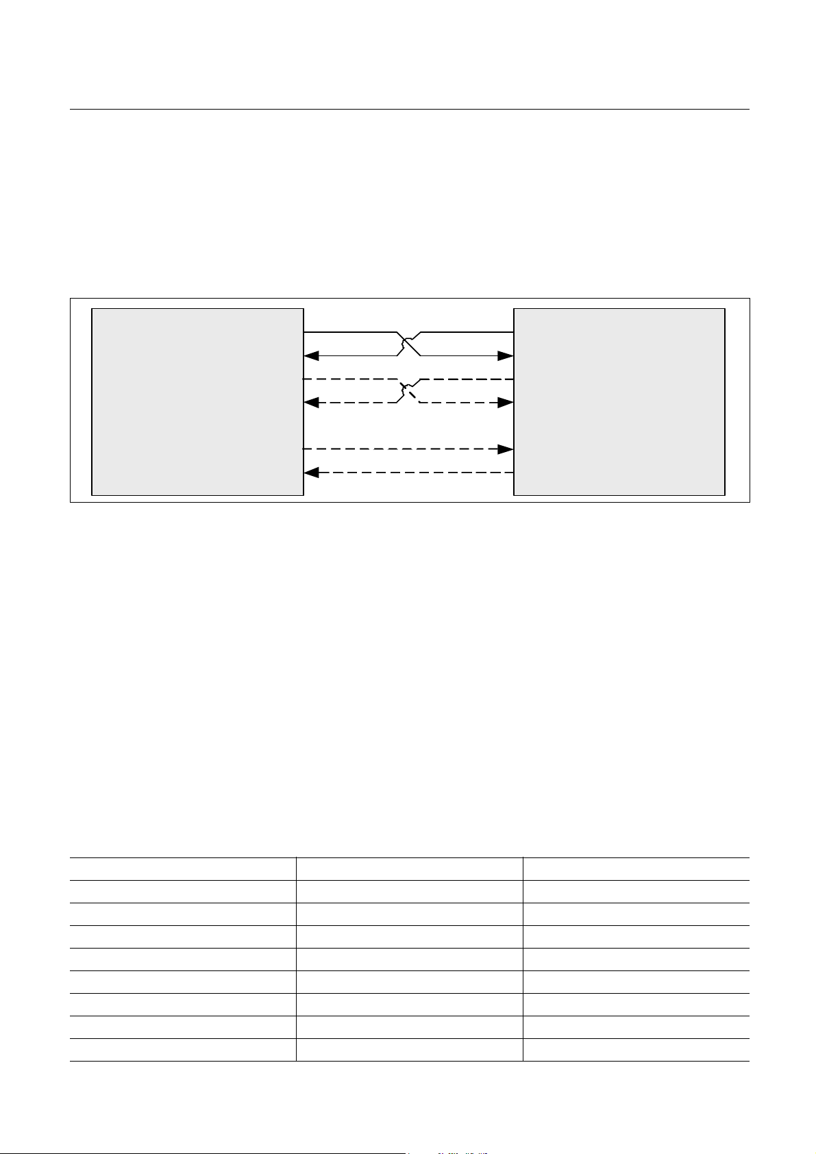
Host PAN1322
WAKEUP_HOST
Figure 4 UART Interface
UARTTXD
UARTRXD
UARTRTS
UARTCTS
WAKEUP_BT
UARTTXD
UARTRXD
UARTRTS
UARTCTS
P0.14 input
P0.0 output
3.1.1 UART
The lines UARTTXD and UARTRXD are used for commands, responses and data. The lines UARTRTS and
UARTCTS are used for hardware flow control. A separate supply voltage, VDDUART, defines the UART reference
levels to fit any system requirements.
3.1.1.1 Baud Rates
The UART baud rate can be configured with the BD_DATA parameter UART_Baudrate. The module is
programmed for a default baudrate of 115200 baud. Reprogramming of the EEPROM configuration is possible by
AT commands at manufacturing time of the end product. The baudrate written to EEPROM will be used each time
PAN1322-SPP starts or, HW or SW reset is done.
The host is also able to change the baudrate temporarily with an AT command. This baudrate is used by
PAN1322-SPP until a HW or SW reset is done, when it will change back to the baudrate stored in the EEPROM.
The supported baud rates are listed in Table 3 together with the small deviation error that results from the internal
clock generation.
Table 2 UART Baud Rates
Wanted Baud Rate Real Baud Rate Deviation Error (%)
9600
19200 19230 0.16
38400 38461 0.16
57600 57522 -0.14
115200 115044 -0.14
230400 230088 -0.14
460800 464285 0.76
921600 928571 0.76
User’s Manual 16 Revision 1.3, 2013-08-14
Hardware Description
9615 0.16
 Loading...