

Page 1
ORDER NO.CHM0602003CE
Portable DVD/CD PLAYER
DVD-LS91PP
RAE1905Z-3C Mechanism Series
Colour
(S).................Silver Type
B12
Specifications
Operating temperature
range: +5 to +35°C (+41 to +95°F)
Operating humidity range: 5-85% RH (no condensation)
Region number: Region No.1
Discs played
[8cm (3”) or 12cm (5”)]:
Signal system: NTSC
DVD (DVD-Video)
DVD-RAM [DVD-VR, JPEG(*4,6,7),
MP3(*2,6)]
DVD-R [DVD-Video, DVD-VR,
JPEG(*4,6,7), MP3(*2,6)]
DVD-R DL (DVD-Video, DVD-VR)
DVD-RW [DVD-Video, DVD-
VR,JPEG(*4,6,7), MP3(*2,6)]
+R/RW (Video)
+R DL (Video)
CD, CD-R/RW [CD-DA, Video-CD,
SVCD(*1), MP3(*2, 6), WMA(*3, 6),
JPEG (*4,6,7), HighMAT Level 2
(Audio and Image)]
*1: Conforming to IEC62107
*2: MPEG-1 Layer3, MPEG-2 Layer3
*3: Windows Media Audio Ver9.0 L3.
Not compatible with Multiple Bit Rate
(MBR)
*4: Exif Ver 2.1 JPEG Baseline files
Picture resolution: between 160×120
and 6144×4096 pixels (sub sampling
is 4:2:2, 4:2:0 or 4:4:4)
*6: The total combined maximum
number of recognizalbe audio and
picture contents and groups: 4000
audio and picture contents and 400
groups.
*7: Extremely long and slender
pictures may not be displayed.
© 2006 Matsushita Electric Industrial Co., Ltd. All
rights reserved. Unauthorized copying and
distribution is a violation of law.
Page 2

A
A
DVD-LS91PP
LCD screen: 9” -Si, TFT wide-screen LCD
Composite-video output/
input:
Output/input level: 1Vp-p (75W)
Output/input terminal: Mini-jack
Number of terminals: 1system (output/input selectable)
Audio output/input:
Output/input level: 1.5Vrms (1kHz, 0dB, 10kW)
Output/input terminal: Stereo mini-jack
Number of terminals: 1system (output/input selectable)
Audio performance:
(1) Frequency response:
lDVD (linear audio): 4Hz-22kHz (48kHz sampling)
4Hz-44kHz (96kHz sampling)
lCD audio: 4Hz-20kHz
(2) S/N ratio:
lCD audio: 115dB
(3) Dynamic range:
lDVD (linear audio): 98dB
lCD audio: 97dB
(4) Total harmonic distortion:
lCD audio: 0.008%
Digital audio output:
Optical digital output: Mini optical terminal
Number of terminals: 1system
(also used for audio output/input)
Headphone output:
Output: Stereo mini-jack
Number of terminals: 2systems
Battery duration:
*CGR-H713: Option
*Room temperature
*using headphone
When brightness is set to “-5” while
playing DVD: 6 hours (CGR-H712)
/10 hours (CGR-H713)
When brightness is set to “0” while
playing DVD: 4 hours (CGR-H712)
/7 hours (CGR-H713)
When brightness is set to “+5” while
playing DVD: 3 hours (CGR-H712)
/5 hours (CGR-H713)
When LCD panel is off while DVD
playing: 10 hours (CGR-H712)
/15 hours (CGR-H713)
Battery recharge time (at
20°C)
8 hours (CGR-H712)
/10 hours (CGR-H713)
Pickup:
Wave length: 662nm/ 785nm (DVD/CD)
Laser power: CLASS 2/ CLASS 1 (DVD/CD)
Power supply: DC 12V (DC IN terminal) /
DC 7.2V (Exclusive battery terminal)
Power consumption
13W (Unit only: 10W)
(Using included AC adaptor):
Power consumption in
0.3W
Standby mode
(Using included AC adaptor):
Power consumption in
13W
Recharge mode
(Using included AC adaptor):
AC adaptor:
Power source:
C 100-240V, 50/60Hz
Power consumption: 28W
DC output: 12V, 1.5A
Car DC adaptor:
DC output: 12V 2A (Vehicle with 12V battery
only)
Battery pack CGR-H712
(lithium ion):
Voltage: 7.2V
Capacity: 4500mAh
Dimensions (excluding
protrusions and battery):
235.4(W) x 179.2(D) x 46.0*(H) mm
9
/32”(W)x71/16”(D)x113/16”(H)]
[9
61
*24.3mm (
[D=185.0mm (7
[H=51.5mm (2
/64”) at lowest point
9
/32”) including battery]
1
/32”) including battery]
Mass (including battery): approximately 1094g (38.59 oz)
solder:
This model uses lead free solder (PbF).
Note
Specifications are subject to change without notice.
Mass and dimensions are approximate.
Manufactured under license from Dolby Laboratories.
“Dolby“ and the double-D symbol are trademarks of Dolby
Laboratories.
“DTS“ and “DTS 2.0+ Digital Out” are trademarks of Digital Theater
Systems, Inc.
pparatus Claims of U.S. Patent Nos. 4,631,603, 4,577,216, and
4,819,098, licensed for limited viewing uses only.
This product incorporates copyright protection technology that is
protected by method claims of certain U.S. patents and other
intellectual property rights owned by Macrovision Corporation and
other rights owners. Use of this copyright protection technology
must be authorized by Macrovision Corporation, and is intended for
home and other limited viewing uses only unless otherwise
authorized by Macrovision Corporation. Reverse engineering or
disassembly is prohibited.
Windows Media, and the Windows logo are trademarks, or
registered trademarks of Microsoft Corporation in the United States
and/or other countries.
WMA is a compression format developed by Microsoft Corporation.
It achieves the same sound quality as MP3 with a file size that is
smaller than that of MP3.
MPEG Layer-3 audio decoding technology licensed from
Fraunhofer llS and Thomson multimedia.
HighMAT™ and the HighMAT logo are either trademarks or
registered trademarks of Microsoft Corporation in the United States
and/or other countries.
2
Page 3
DVD-LS91PP
CONTENTS
Page Page
1 SAFETY PRECAUTIONS 5
1.1. GENERAL GUIDELINES
2 PREVENTION OF ELECTRO STATIC DISCHARGE (ESD) TO
ELECTROSTATICALLY SENSITIVE (ES) DEVICES
3 PRECAUTION OF LASER DIODE
4 HOW TO REPLACE THE LITHIUM BATTERY
5 LITHIUM ION BATTERY
6 Service caution based on legal restrictions
6.1. General description about Lead Free Solder (PbF)
7 HANDLING PRECAUTIONS FOR TRAVERSE DECK
7.1. Handling of optical pickup
7.2. Grounding for electrostatic breakdown prevention
8 DISASSEMBLY, REASSEMBLY AND SERVICE POSITION
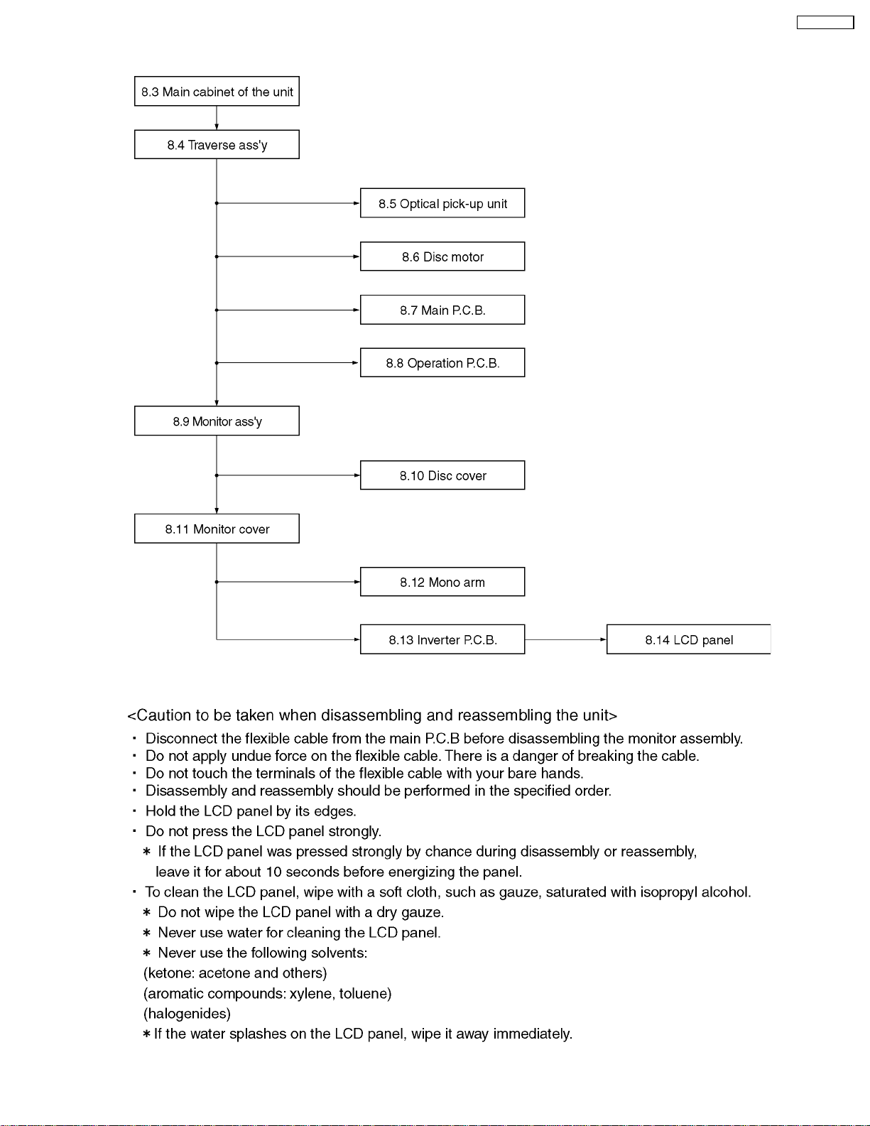
8.1. Disassembly
8.2. P.C.B. location
8.3. Main cabinet of the unit
8.4. Traverse assembly
8.5. Optical pick-up unit
8.6. Disc motor
8.7. Main P.C.B.
8.8. Operation P.C.B.
8.9. Monitor assembly
8.10. Disc cover
8.11. Monitor cover
8.12. Mono arm
8.13. Inverter P.C.B.
8.14. LCD panel
8.15. Replacing the fuse in the car dc adaptor
8.16. Service position
9 SELF-DIAGNOSIS FUNCTION AND SERVICE MODE
9.1. Optical Pickup Breakdown Diagnosis
9.2. UHF displays
9.3. Service Mode Table 1
9.4. DVD Self Diagnostic Function-Error Code
9.5. Last Error Code saved during NO PLAY
9.6. Service mode table
9.7. Lens cleaning
10 SERV ICE PREC AUTIONS
10.1. Recovery after the dvd player is repaired
10.2. Firmware version-up of the DVD player
11 ADJUSTMENT PROCEDUR ES
11.1. Service Tools and Equipment
11.2. Important points in adjustment
11.3. Storing and Handling Test Discs
11.4. Optical adjustment
11.5. Electrical adjustment (LCD)
10
11
12
12
13
14
14
15
15
15
16
16
17
18
18
18
19
20
20
21
22
22
26
26
29
30
30
30
31
31
31
31
32
34
11.6. Electrical check (Video output check)
5
12 Abbreviation s
13 VOL TAGE CHART
5
6
7
7
8
8
9
9
9
13.1. MAIN P.C.B.
13.2. INVERTER P.C.B.
14 BLOCK DIAGRAM
14.1. OVERALL BLOCK DIAGRAM
14.2. POWER SUPPLY BLOCK DIAGRAM
14.3. SERVO BLOCK DIAGRAM
14.4. AUDIO BLOCK DIAGRAM
14.5. VIDEO BLOCK DIAGRAM
15 INTERCONN ECTIO N SCHEMATIC DIAGRAM & SCHEMATIC
DIAGRAM NOTES
15.1. INTERCONNECTION SCHEMATIC DIAGRAM
15.2. SCHEMATIC DIAGRAM NOTES
16 SCHE MATIC DIAGRAM
16.1. CHARGE BATTERY SECTION (MAIN P.C.B. (1/10))
SCHEMATIC DIAGRAM
16.2. POWER SUPPLY SECTION (MAIN P.C.B. (2/10))
SCHEMATIC DIAGRAM
16.3. SERVO SECTION (MAIN P.C.B. (3/10)) SCHEMATIC
DIAGRAM
16.4. OPTICAL PICK UP SECTION (MAIN P.C.B. (4/10))
SCHEMATIC DIAGRAM
16.5. DV3 SECTION (MAIN P.C.B. (5/10)) SCHEMATIC
DIAGRAM
16.6. VIDEO OUT SECTION (MAIN P.C.B. (6/10)) SCHEMATIC
DIAGRAM
16.7. AUDIO OUT SECTION (MAIN P.C.B. (7/10)) SCHEMATIC
DIAGRAM
16.8. OPERATION SECTION (MAIN P.C.B. (8/10))
SCHEMATIC DIAGRAM
16.9. LCD IF SECTION (MAIN P.C.B. (9/10)) SCHEMATIC
DIAGRAM
16.10. XBS SECTION (MAIN P.C.B. (10/10)) SCHEMATIC
DIAGRAM
16.11. OPERATION SECTION (OPERATION P.C.B.)
SCHEMATIC DIAGRAM
16.12. INVERTER SECTION SCHEMATIC DIAGARAM
17 CIRC UIT BOARD ASSEMBLY
17.1. MAIN P.C.B. (1/2) (COMPONENT SIDE)
17.2. MAIN P.C.B. (2/2) (FOIL SIDE)
17.3. OPERATION & INVERTER P.C.B.
18 EXPL ODED VIEW S
18.1. Casing Parts & Mechanism Section Exploded View
18.2. Mechanism Section Exploded View
35
36
38
38
41
43
43
44
45
46
47
49
49
50
51
51
52
53
54
55
56
57
58
59
60
61
62
63
63
64
65
67
67
68
3
Page 4

DVD-LS91PP
18.3. Packing & Accessories Exploded View 69 19 REPLACEMENT PARTS LIST 70
4
Page 5
DVD-LS91PP
1 SAFETY PRECAUTIONS
1.1. GENERAL GUIDELINES
1. When servicing, observe the original lead dress. If a short circuit is found, replace all parts which have been overheated or
damaged by the short circuit.
2. After servicing, see to it that all the protective devices such as insulation barriers, insulation papers shields are properly
installed.
3. After servicing, make the following leakage current checks to prevent the customer from being exposed to shock hazards.
1.1.1. LEAKAGE CURRENT COLD
CHECK
1. Unplug the AC cord and connect a jumper between the two
prongs on the plug.
2. Measure the resistance value, with an ohmmeter, between
the jumpered AC plug and each exposed metallic cabinet
part on the equipment such as screwheads, connectors,
control shafts, etc. When the exposed metallic part has a
return path to the chassis, the reading should be between
1MW and 5.2MW .
When the exposed metal does not have a return path to
the chassis, the reading must be
.
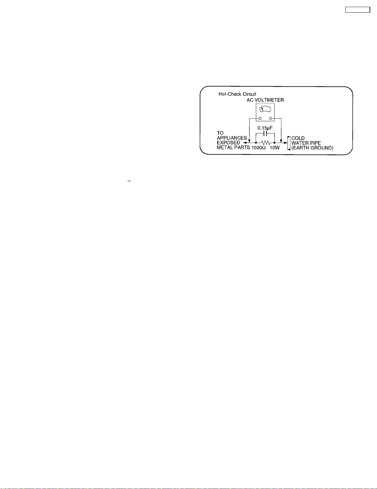
1.1.2. LEAKAGE CURRENT HOT CHECK
1. Plug the AC cord directly into the AC outlet. Do not use an
isolation transformer for this check.
2. Connect a 1.5kW, 10 watts resistor, in parallel with a 0.15µF
capacitors, between each exposed metallic part on the set
and a good earth ground such as a water pipe.
3. Use an AC voltmeter, with 1000 ohms/volt or more
sensitivity, to measure the potential across the resistor.
4. Check each exposed metallic part, and measure the
voltage at each point.
5. Reverse the ACplug in theAC outlet and repeat each of the
above measurements.
6. The potential at any point should not exceed 0.75 volts
RMS. A leakage current tester (Simpson Model 229 or
equivalent) may be used to make the hot checks, leakage
current must not exceed 1/2 milliamp. In case a
measurement is outside of the limits specified, there is a
possibility of a shock hazard, and the equipment should be
repaired and rechecked before it is returned to the
customer.
2 PREVENTION OF ELECTRO STATIC DISCHARGE (ESD)
TO ELECTROSTATICALLY SENSITIVE (ES) DEVICES
Some semiconductor (solid state) devices can be damaged easily by static electricity. Such components commonly are called
Electrostatically Sensitive (ES) Devices. Examples of typical ES devices are integrated circuits and some field-effect transistors and
semiconductor "chip" components. The following techniques should be used to help reduce the incidence of component damage
caused by electro static discharge (ESD).
1. Immediately before handling any semiconductor component or semiconductor-equipped assembly, drain off any ESD on your
body by touching a known earth ground. Alternatively, obtain and wear a commercially available discharging ESD wrist strap,
which should be removed for potential shock reasons prior to applying power to the unit under test.
2. After removing an electrical assembly equipped with ES devices, place the assembly on a conductive surface such as alminum
foil, to prevent electrostatic charge buildup or exposure of the assembly.
3. Use only a grounded-tip soldering iron to solder or unsolder ES devices.
4. Use only an anti-static solder removal device. Some solder removal devices not classified as "anti-static (ESD protected)" can
generate electrical charge sufficient to damage ES devices.
5. Do not use freon-propelled chemicals. These can generate electrical charges sufficient to damage ES devices.
6. Do not remove a replacement ES device from its protective package until immediately before you are ready to install it. (Most
replacement ES devices are packaged with leads electrically shorted together by conductive foam, alminum foil or comparable
conductive material).
7. Immediately before removing the protective material from the leads of a replacement ES device, touch the protective material
to the chassis or circuit assembly into which the device will be installed.
Caution
Be sure no power is applied to the chassis or circuit, and observe all other safety precautions.
5
Page 6
DVD-LS91PP
8. Minimize bodily motions when handling unpackaged replacement ES devices.(Otherwise hamless motion such as the brushing
together of your clothes fabric or the lifting of your foot from a carpeted floor can generate static electricity (ESD) sufficient to
damage an ES device).
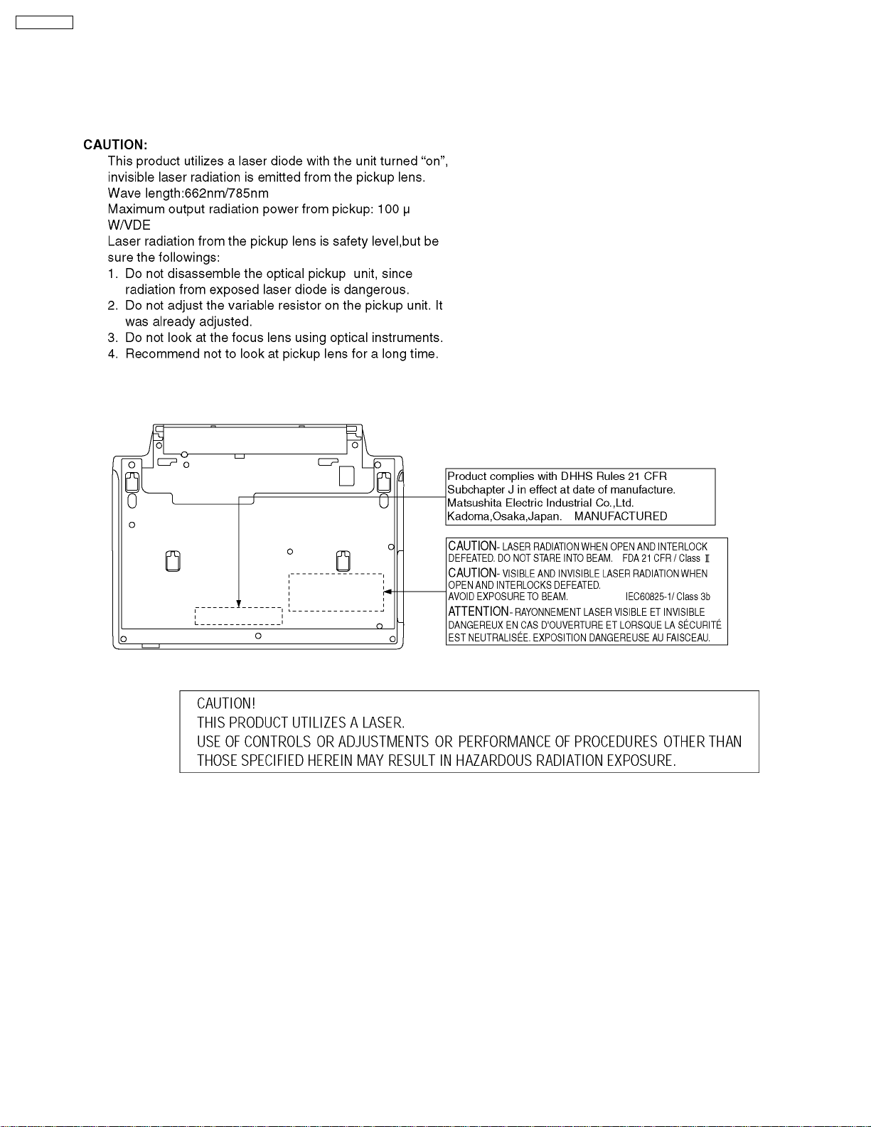
3 PRECAUTION OF LASER DIODE
6
Page 7
4 HOW TO REPLACE THE LITHIUM BATTERY
This model is using a lithium battery for the remote control ass’y.
NOTE:
The lithium battery is a critical component. ( Type No.: CR2025 Manufactured by Panasonic. )
It must never be subjected to excessive heat or discharge.
It must therefore only be fitted in equipment designed specifically for its use.
Replacement batteries must be of the same type and manufacture.
They must be fitted in the same manner and location as the original battery, with the correct polarity contacts observed.
Do not attempt to re-charge the old battery or re-use it for any other purpose.
It should be disposed of in waste products destined for burial rather than incineration.
DVD-LS91PP
5 LITHIUM ION BATTERY
7
Page 8

DVD-LS91PP
6 Service caution based on legal restrictions
6.1. General description about Lead Free Solder (PbF)
The lead free solder has been used in the mounting process of all electrical components on the printed circuit boards used for this
equipment in considering the globally environmental conservation.
The normal solder is the alloy of tin (Sn) and lead (Pb). On the other hand, the lead free solder is the alloy mainly consists of tin
(Sn), silver (Ag) and Copper (Cu), and the melting point of the lead free solder is higher approx.30 degrees C (86 F) more than that
of the normal solder.
Definition of PCB Lead Free Solder being used
The letter of “PbF” is printed either foil side or components side on the PCB
using the lead free solder. (See right figure)
Service caution for repair work using Lead Free Solder (PbF)
- The lead free solder has to be used when repairing the equipment for which the lead free solder is used.(Definition: The letter
of "PbF" is printed on the PCB using the lead free solder.)
- To put lead free solder, it should be well molten and mixed with the original lead free solder.
- Remove the remaining lead free solder on the PCB cleanly for soldering of the new IC.
- Since the melting point of the lead free solder is higher than that of the normal lead solder, it takes the longer time to melt the
lead free solder.
- Use the soldering iron (more than 70W) equipped with the temperature control after setting the temperature at 350+-30
degrees C (662+-86 F).
Recommended Lead Free Solder (Service Parts Route.)
- The following 3 types of lead free solder are available through the service parts route.
RFKZ03D01K-----------(0.3mm 100g Reel)
RFKZ06D01K-----------(0.6mm 100g Reel)
RFKZ10D01K-----------(1.0mm 100g Reel)
Note
* Ingredient: tin (Sn) 96.5%, silver (Ag) 3.0%, Copper (Cu) 0.5%, Cobalt (Co) / Germanium (Ge) 0.1 to 0.3%
8
Page 9
7 HANDLING PRECAUTIONS FOR TRAVERSE DECK
DVD-LS91PP
The laser diode in the optical pickup may break down due to
potential difference caused by static electricity of clothes or
human body.
So be careful of electrostatic break down during repair of the
optical pickup.
It has already been adjusted.
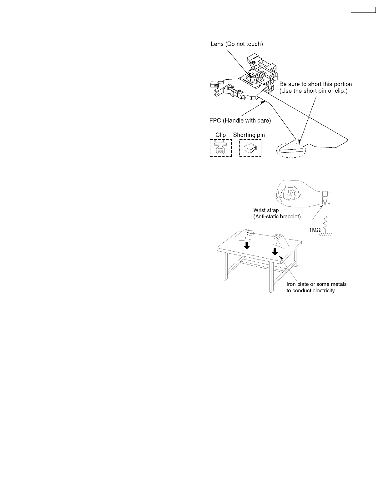
7.1. Handling of optical pickup
1. Do not subject the optical pickup to static electricity as it is
extremely sensitive to electrical shock.
2. To prevent the breakdown of the laser diode, an antistatic
shorting pin is inserted into the flexible board (FPC Board).
When removing or connecting the short pin, finish the job in
as short times as possible.
3. Be careful not toapply excessive stressto the flexible board
(FPC Board).
4. Do not turn the variable resistor (Laser power adjustment).
7.2. Grounding for electrostatic breakdown prevention
1. Human body grounding
Use the antistatic wrist strap to discharge the static
electricity from your body.
2. Work table grounding
Put a conductive material (sheet) or steel sheet on the area
where the optical pickup is placed and ground the sheet.
Caution
The static electricity of your clothes will not be grounded
through the wrist strap. So take care not to let your
clothes touch the optical pickup.
9
Page 10
DVD-LS91PP
8 DISASSEMBLY, REASSEMBLY AND SERVICE POSITION
10
Page 11
8.1. Disassembly
DVD-LS91PP
11
Page 12
DVD-LS91PP
8.2. P.C.B. location
8.3. Main cabinet of the unit
<Removing battery pack>
Release the lock lever and remove the battery pack in the
direction of the arrow.
1. Remove the 13 screws from the bottom of the unit.
2. Release the latches and remove the bottom cabinet.
12
Page 13
8.4. Traverse assembly
8.4.1. Removing traverse assembly
1. Solder the 2 laser short lands on the flexible cable.
2. Unlock the connectors and remove the flexible cables.
DVD-LS91PP
8.4.2. Reinstalling traverse assembly
1. Reinstall the traverse assembly to the specified pin of the
unit.
2. Reinstall the flexible cable of the optical pickpup unit and
lock it securely.
3. Remove the solder of each laser short land of the flexible
cable.
Caution:
Remove the solders completely: otherwise the laser
diode won’t emit light.
4. Reinstall the spindle flexible cable as shown figure.
13
Page 14
DVD-LS91PP
8.5. Optical pick-up unit
8.5.1. Removing optical pick-up unit
8.5.2. Reinstalling optical pick-up unit
The optical pick-up unit is factory adjusted. Do not touch the
adjustment screw.
1. Reassemble the disassembled parts in the reverse order of
disassembly.
2. When reinstalling the traverse assembly on the main unit
after installing the optical pick-up unit, make sure to remove
the solder from each of the two laser short lands on the
flexible cable.
Caution:
· Remove the solders completely; otherwise the laser
diode won´t emit light.
· After replacing the optical pick-up unit, check the quality
of images played back and make optical adjustment.
8.6. Disc motor
8.6.1. Removing disc motor
1. Remove the adjustment screws A, B, and C.
2. Remove the disc motor.
Make sure that the traverse assembly removed before trying to
remove the optical pick-up unit.
When removing the traverse assembly, solder the two laser
short lands on the flexible cable of the optical pick-up unit.
1. Remove the two screws securing the main shaft retainer.
2. Remove the main shaft retainer.
3. Slide the main shaft in the direction indicated by the arrow
to remove the optical pick-up unit.
8.6.2. Caution to be taken when
replacing the disc motor
1. The mounting screws of the disc motor also serve as
adjustment screws. When reinstalling the disc motor, first
turn the screws A, B, and C as far as they go by usual force
to secure them (do not overtighten).
2. Back off the adjustment screws Aand C two complete turns
and secure them.
3. Back off the adjustment screw B one and a half turns and
secure them.
· This makes it nearly possible to play back disks and
adjust the jitter.
Thereafter, adjust the adjustment screws C and A as
indicated.
14
Page 15
8.7. Main P.C.B.
1. Unlock the connector and remove the flexible cable.
2. Remove the connector.
3. Remove the 4 screws and remove the main P.C.B..
DVD-LS91PP
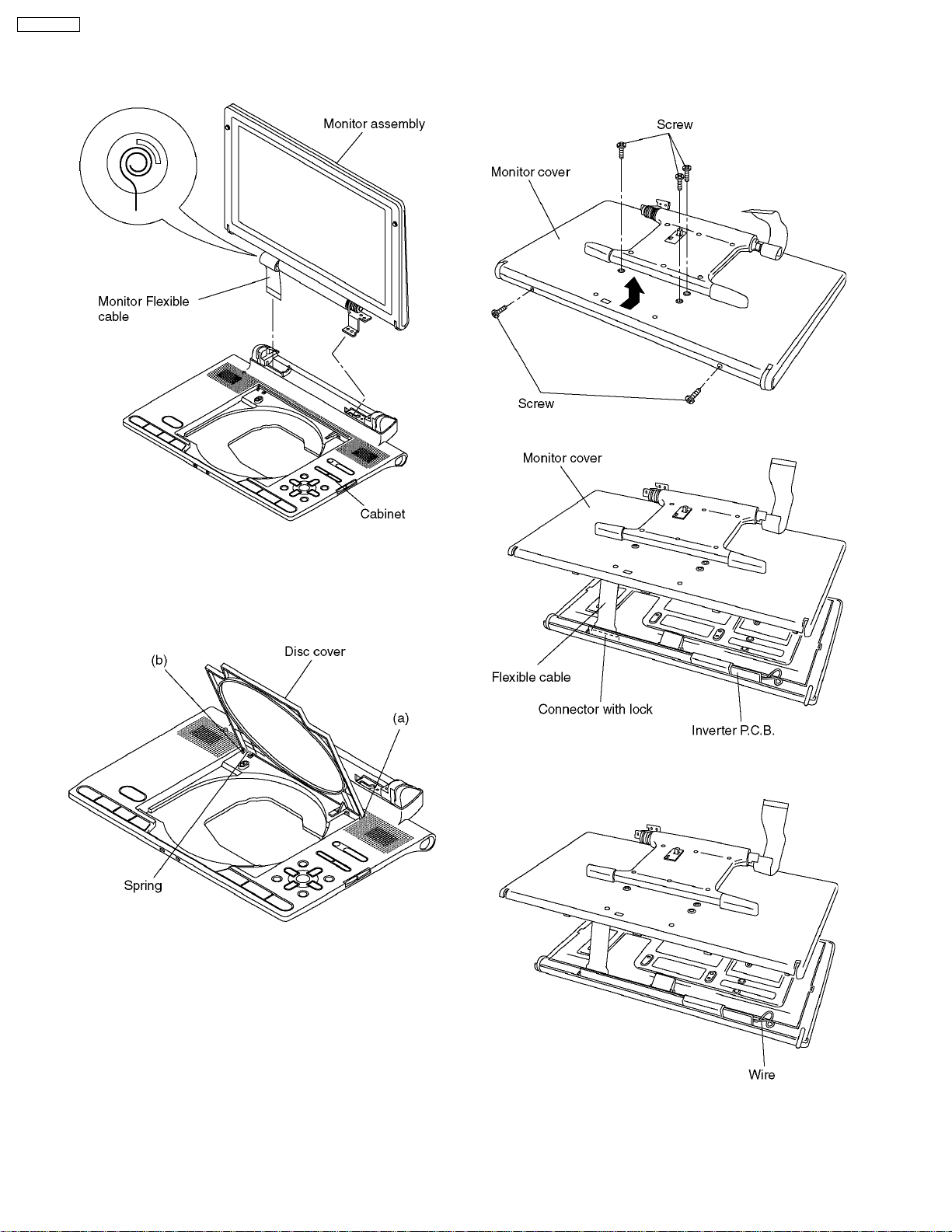
8.9. Monitor assembly
1. Unlock the connector and remove the flexible cable.
2. Remove the 3 screws.
8.8. Operation P.C.B.
1. Remove the connector.
2. Remove the 6 screws and remove the operation P.C.B.
3. Release the latches and remove the hinge cover.
4. Remove the screw and remove the monitor assembly.
15
Page 16
DVD-LS91PP
<Caution to be taken when installing monitor assembly>
1. Roll the flexible cable as shown figure.
2. Install the monitor assembly on the cabinet.
8.11. Monitor cover
1. Remove the 5 screws
2. Remove the monitor cover into the direction of the arrow.
3. Unlock the connector and remove the flexible cable.
8.10. Disc cover
1. Remove the disc cover in order of (a) and (b).
Caution:
Please don’t lose the spring
<Caution to be taken when installing monitor cover>
Please do not nip the wire.
16
Page 17
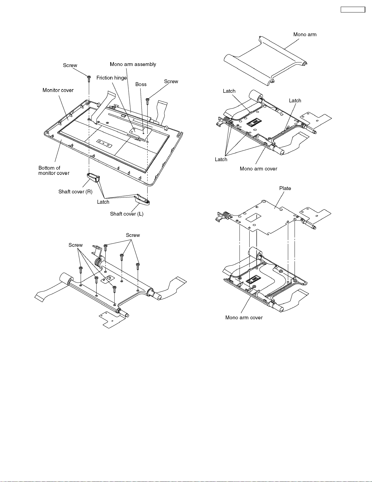
8.12. Mono arm
1. Remove the 2 screws.
2. Release the latches and remove the shaft covers.
3. Release the friction hinge from boss and remove the mono
arm assembly.
DVD-LS91PP
5. Release the latches and remove the mono arm
6. Remove the plate.
4. Remove the 6 screws.
17
Page 18
DVD-LS91PP
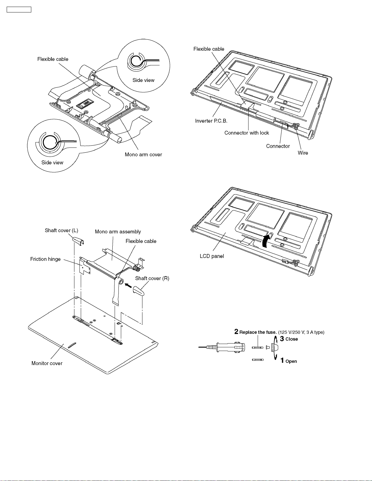
<Caution to be taken when installing mono arm>
1. Roll the flexible cables as shown figure and install it to
mono arm cover.
8.13. Inverter P.C.B.
1. Unlock the connector and remove the flexible cable.
2. Remove the connector and remove the inverter P.C.B.
8.14. LCD panel
2. Install mono arm.
3. Roll 3 turns of the flexible cable and Install the shaft
cover (R) to flexible cable.
4. Pass the flexible cable and the friction hinge into the
holes in the monitor cover.
5. Install the shaft covers to monitor cover.
1. Remove the LCD panel into the direction of the arrow.
8.15. Replacing the fuse in the car
dc adaptor
· Replace only with the specified 125V/250V, 3A fuse. Use of
any other type can cause fire.
18
Page 19
DVD-LS91PP
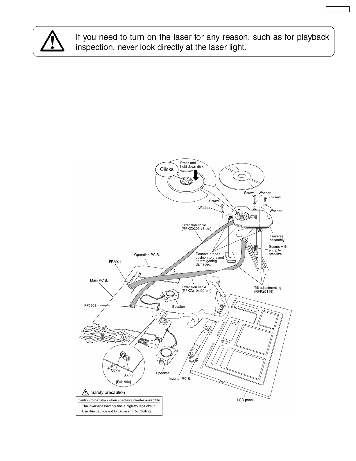
8.16. Service position
8.16.1. Board checks
1. Connect the main P.C.B and the traverse assembly with an extension cable.
2. Install the traverse assembly to the tilt adjustment jig using three screws and three washers.
Caution:
· Remove the rubber cushion from the traverse assembly to prevent it from getting damaged.
3. Install a dick on the traverse assembly.
Caution:
· Make sure the disk is securely installed on the disk motor.
4. Remove the main P.C.B., operation P.C.B., inverter P.C.B., and LCD panel as shown below.
5. The disk cannot be played back with the disk cover removed. Press and hold down the S5201 and S5202. (Secure with
cellulose tape.)
19
Page 20
DVD-LS91PP
9 SELF-DIAGNOSIS FUNCTION AND SERVICE MODE
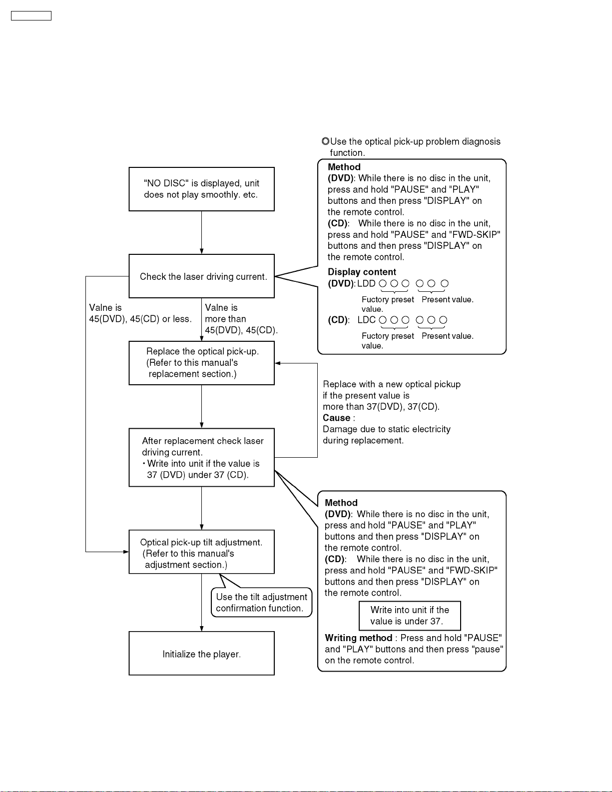
9.1. Optical Pickup Breakdown Diagnosis
As a new feature, this unit has an “optical pick-up problem diagnosis function” and “a tilt adjustment confirmation function” built
in. Use the following procedure to efficiently determine the problem and adjust tilt.If "NO DISC" is displayed, before exchanging
the optical pick-up, carry out problem diagnosis first. If the present laser driving current is over 55, the optical pick-up may need
to be exchanged.
Note:
Carry out diagnosis within 3 minutes of turning the unit on. (The player’s current can increase as it warms up, so turn the unit
off and allow it to cool down before diagnosis.)
20
Page 21
Cautions to be taken when replacing the optical pickup
The optical pickup may break down due to the static
electricity of human body. Take proper protection measures
against static electricity before repairing the parts around
the optical pickup. (See the page describing the
PREVENTION OF STATIC ELECTRICITY DISCHARGE.)
1. Do not touch the areas around the laser diode and
actuator.
2. Do not judge the laser diode with a tester. (The tester
will be damaged easily.)
3. It is recommended to use a destaticized soldering iron
DVD-LS91PP
for short-circuiting or removing the laser diode.
(Recommended soldering iron) HAKKO ESD Product
4. Solder the land of the flexible cablein theoptical pickup.
Note:
· When using a soldering iron which is not
destaticized, short-circuit the terminal face of the
flexible case with a clip. After that, short-circuit
the land.
· After the repairing work is completed, remove the
solder according to the correct procedure shown
in this Technical Guide.
9.2. UHF displays
Use the internal service mode for evaluation of malfunctions.
Display Method Display Diagnosis
Items displayed when in use CHECK THE
Press the "0" button on the remote control while holding
down the PAUSE and PLAY buttons on the player.
The last error code generated is saved in the EEPROM
DISC
H01 Inner cover trouble
H02 Spindle servo error
H03 Traverse error
H04 Tracking servo error
H05 Seek error
F0** Disc format error
F1** Disc code error
F2** Decoder LSI error
F5** DSC
F6** ECC error
F7** Microcomputer error
F8** Microcomputer error
Focus error
21
Page 22

DVD-LS91PP
9.3. Service Mode Table 1
The service modes can be activated by pressing various button combination on the player and remote control unit.
Player buttons Remote control unit buttons Application Note
PAUSE
+
PLAY
PAUSE
BWD-SKIP
PLAY
0 Displaying the UHF display F_ _ _ Refer to section 9.4. Self-
5 Jitter check, tilt adjustment
*Display shows xx_yyyzz
"xx" and "zz" shown to the right have nothing to do with the jitter
value. "xx" is the error counter, while "zz" is the focus drive value.
Refer to section 11.4. for Optical Pickup Tilt Adjustment
Procedure.
6 Checking the region numbers and broadcast system
7 Checking the program version Check the IC3001 FLASH
9 Lighting Confirmation Function of Display Tube
DISPLAY Checking the laser drive current Refer to section 8.5.
PAUSE Writing the laser drive current value after replacing the optical
pickup (do not use for anything other than optical pickup
replacement)
The user setting is returned to the state of the factory shipment. Refer to section 9.6.
—
Diagnosis Function (UHF
Display).
Refer to section 11.4.
Optical Pickup Tilt
Adjustment
ROM program.
Optical Pickup
Replacement Procedure.
Initializing the DVD
player.
9.4. DVD Self Diagnostic Function-Error Code
<Displayed during normal operations>
Error code Contents Case of Occurrence Task Remarks
U11 Focus Servo error Dirty disc
CHECK DISK Servo
U15 DVD-R not finalized Servo
U70-1 HDMI/DVI EDID reading error Occurs when connection is HDMI/DVI and EDID data for
U70-2 HDMI/DVI non-HDCP
compliance
U70-3 HDMI/DVI authentication error Occurs when connection is HDMI/DVI and authentication of
H01 Tray loading error Tray movement error. Unable to open. Unable to close. Panel When OPEN:
H02 Spindle error Spindle motor errorFG pulse abnormal. Cable cut, etc. Servo
H03 Traverse motor error Traverse abnormal Servo
H05 Seek time out error Unable to access. TOC reading error, etc.
H07 Driver IC thermal shutdown Spindle motor error (short circuit in between brushes)
Incompatible media
DVD-R and RW not finalized.
Output may result when a pickup error occurs.
the picture receiver cannot be read.
Occurs when connection is HDMI/DVI and the picture
receiver is not compliant with HDCP.
HDCP:Copyright protection technology
Digital video signal encryption method
the picture receiver (using HDCP) failed.
Pickup error, disc error, etc.
Output results when a dirty disc is used.
(Applicable to brush-type spindle motors only)
Servo U11 may also result when
DVD-R is not finalized.
AV
AV
AV
FOPEN->CLOSE->OPEN>H01
When CLOSE:
FCLOSE->OPEN->CLOSE>H01
Servo Changed to U11 from D80
series onward.
Servo
22
Page 23

<Recorded but not displayed during normal>
Error code Contents Case of Occurrence Task Remarks
F010 Set value exceeded parental
value in the designated country
F020 TT_SRPT does not
existÅiRLBN is 0
F021 TT_SRP number is 0 DVD-Video/Audio
F022 Set value exceeds TT_SRP
number
F023 SRP in conformity with VTSN
or VTS_TTN does not exist
F024 Set value exceeds
TT_SRP.PTT_Ns
F030 TTU_SRP number is 0 DVD-Video/Audio
F031 Set value exceeds TTU_SRP
number
F041 PGCI_SRP number is 0 DVD-Video/Audio
F042 Set value exceeds PGCI_SRP
number
F051 Set value exceeds TMAP_SRP
number
F052 Set TMAP_SA is 0 DVD-Video/Audio
F053 MAP_EN number is 0 DVD-Video/Audio
F060 C_POSIT exists, but PGMAP
does not exist in PGC
F061 C_POSIT exists, but PG
number in PGC is 0
F062 Set value exceeds PG number
in PGC
F063 C_POSIT exists, but C_PBIT
does not exist in PGC
F064 C_POSIT exists, but Cell
number in PGC is 0
F065 Set Cell number is 0 DVD-Video/Audio
DVD-Video
Disc management data error
(Error in management data related to viewing restrictions)
DVD-Video/Audio
Disc management data error
(Error in title-related management data)
Disc management data error
(Error in title-related management data)
DVD-Video/Audio
Disc management data error
(Error in title-related management data)
DVD-Video/Audio
Disc management data error
(Error in title-related management data)
DVD-Video/Audio
Disc management data error
(Error in chapter-related management data)
Disc management data error
(Error in title-related management data)
DVD-Video/Audio
Disc management data error
(Error in title-related management data)
Disc management data error
(Error in title-related or menu-related management data)
DVD-Video/Audio
Disc management data error
(Error is title-related management data)
DVD-Video/Audio
Disc management data error
(Error in management data for time-search)
Disc management data error
(Error in management data for time-search)
Disc management data error
(Error in management data for time-search)
DVD-Video/Audio
Disc management data error
(Error in title-related management data)
DVD-Video/AudioDisc management data error(Number of
chapter is 0 or management data is arranged in violation of
specifications.)
DVD-Video/Audio
When one of the following conditions applies
· Disc management data error
(Error in title-related or chapter-related management
data)
· Management data is arranged in violation of
specifications.
DVD-Video/Audio
Disc management data error
(Error in title-related or chapter-related management data)
DVD-Video/Audio
Disc management data error
(Chapter number is 0)
Disc management data error
(Chapter number is 0)
Disc
Disc
Disc
Disc May occur when a wrong
number is set
(when the set number
exceeds the maximum
number of titles in the disc).
Disc
Disc May occur when a wrong
chapter number is set
(when the set number
exceeds the maximum
number of chapters in the
disc).
Disc
Disc May occur when a wrong
title number is set
(when the set number
exceeds the maximum
number of titles in the disc).
Disc
Disc May occur when a wrong
title number is set
(when the set number
exceeds the maximum
number of titles in the disc).
Disc
Disc
Disc
Disc
Disc
Disc May occur when a wrong
chapter number is set
(when the set number
exceeds the maximum
number of chapters in the
title).
Disc
Disc
Disc
DVD-LS91PP
23
Page 24

DVD-LS91PP
Error code Contents Case of Occurrence Task Remarks
F066 Set value exceeds cell number
in PGC
DVD-Video/Audio
Disc management data error
(Chapter number is 0)
Disc May occur when a wrong
chapter number is set
(when the set number
exceeds the maximum
number of chapters in the
title).
F067 Must be a block cell DVD-Video/Audio
Disc
Disc management data error
(Data error related to angles in the title)
F070 Not NV_PCK data DVD-Video/Audio
Disc
Disc management data error
(Management data or its arrangement is in violation of
specifications)
F080 Searched Cell number is not
found
DVD-Video/Audio
Disc management data error
(Chapter number is 0)
Disc May occur when a wrong
chapter number is set
(when the set number
exceeds the maximum
number of chapters in the
title).
0xF0C0 Management data error, no
playback file
<No contents (management data and playback files do not
exist)>
Disc Defined in DEFMAIN.H
Set under the following conditions
· When a DVD-Video/VR/Audio management data
contains an error
· When playback contents do not exist
(Search continues to the end and no contents error
results when SD and PCF file management data error
exists)
0xF0C1 Disallowed region code DVD-Video
Disc Defined in DEFMAIN.H
Disallowed through region code
DVD-Video disc region code different from the player region
code was set at the time of playback.
0xF0C2 PAL playback disallowed DVD-Video/VR
Disc Defined in DEFMAIN.H
May be displayed when
EEPROM was falsified.
Set when a DVD-Video/VR disc containing a PAL program
is set on a model that plays no PAL contents.
0xF0C3 All titles not playable under the
parental lock
0xD0C5 VCD/CDÅFCD-ROM other
than CD-DA disallowed
DVD-VideoSet when viewing restrictions disallows
playback.
Playback disallowed for a CD not compliant with the player
May be set when disc is not CD-DA, and it contains no file
such as an MP3/WMA file compliant with the player.
Disc Defined in DEFMAIN.H
Disc Defined in DEFMAIN.H
This error is rarely recorded
even when a disc described
left is set. The error exists
for a reason unknown.
F0C6 SD card: FAT error SD card format not readable
The card might have been formatted on a Windows PC.
F0C7 SD card: physical error <Physical card error>
Disc Mounted on D86-generation
and newer models
Drive
The SD card may be destroyed physically.
Possible insertion of a card other than SD card/MMC
Only mini SD card adapter may be inserted
F0C8 SD card : master boot record
error
F0E5 Firm file reading error at the
time of downloading
F103 Illegal Highlight Position Occurs mainly in cases where the disc violates
SD card is not destroyed physically, but reading not normal.
SD card formatting may correct the error.
DFD disc reading error
(Firm rewrite data was not read correctly)
Drive Mounted on D86-generation
and newer models
Disc
AV ILL_HLPOS
specifications.
Occurs when a location set for highlighting does not exist
on a DVD-V disc.
F4FF Compulsory initialization failure
(time-out)
Compulsory initialization failed despite a wrong EEPROM
value
UI Defined in DEFMAIN.H
F500 DSC error Servo LSI error Servo
F501 DSC not ready Error Servo
F502 DSC time-out error Servo LSI error, servo adjustment error Servo
F505 DSC attention error Servo error Servo
F506 Invalid media Unsupported media, data is unreadable Servo
0x9010 DSC command escape OPEN request Servo Not an error
0x9020 Unrecorded field Entered an unrecorded field on a multi-session CD-R, RW Servo Not an error
F0BB No DVD-R playback Copyright protection (CSS) exists for DVD-R.
Drive Registration
DVD-R does not play back because it is an illegal copy.
F0BC No DVD-RAM playback Copyright protection (CSS) exists for DVD-RAM.
Drive Registration
DVD-RAM does not play back because it is an illegal copy.
24
Page 25

Error code Contents Case of Occurrence Task Remarks
F0BF No playback because physical
layer cannot be detected
F600 Management data is
inaccessible because of a
demodulation error.
F601 Unstable sector ID was
requested
F603 KEYDET acquisition
impossible due to
demodulation error.
F700 MBX Overflow Incorrect processing error within microcomputer
F701 Message command not
complete error
F702 Message command changed Incorrect processing error within microcomputer
F740 When HDMI device key writing
failed
F750 When the HDMI Device Key
was wrong
F890 Tried to send message during
transmission to AV task
F891 Message transmission to AV
task failed (Mailbox overflow,
etc.)
F893 Flash data falsification error When an error is found in Flash ROM data Sys
F894 EEPROM error When accessing EEPROM failed Sys Subsite value eutered with
F895 Firm type disagreement
(destination mismatch)
F896 Firm type disagreement (non-
existent jumper)
F897 Incomplete initialization When initialization is not performed after firm writing Sys Defined in DEFMAIN.H
F898 Disagreement between the AV
Dec hardware version and the
system controller firm type
F899 Disagreement between system
controller and panel controller
communication specifications
F8A0 Message command is
improper
0xB000 Target file was not found DVD-RAM disc management data error
0xB001 Disc is not DVD-RAM or RW DVD disc management data error Disc Set when UDF
0xA002 For hang-up prevention, no
error.
Media identification impossible
(examples)
1. Detection impossible due to inferior disc non-compliant
with specifications
2. CDV or other unsupported media
3. Disc was inserted upside down.
Data necessary for NaviPack and other navigation transfers
became impossible to acquire due to a damaged disc and
other causes, and playback transfer became impossible.
Attempt was made to access a non-existent disc location
due to authoring record and other errors.
Data for decrypting copyright protection (CSS) became
impossible to acquire due to a damaged disc or other
causes, playback is not possible.
Occurs mainly in cases where microcomputer software has
a problem.
Incorrect processing error within microcomputer
Occurs mainly in cases where microcomputer software has
a problem.
Occurs mainly in cases where microcomputer software has
a problem.
I2C error occurred while writing to Device Key in Tx. AV
Occurs when the wrong Device Key is written into Tx. AV
Player system error Disc Player control software
Player system error Disc Player control software
When the destination and type of used firm differ Sys Defined in DEFMAIN.H
When a jumper falling under no type is set Sys Defined in DEFMAIN.H
When the destination and type of used firm differ Sys
Mismatch in firm/product numbers for the system controller
and panel controller used
Player system error Disc Player control software
(recorded in the DVD-VR format)
CD mediaDisc management data error Disc Set for hang-up prevention
Drive Registration
ECC Registration
ECC Registration
ECC Registration
AV MSG_QOVR
AV MSG_NOTCOMP
AV MSG_CMDCHG
operation is abnormal
operation is abnormal
INITIALI.C immediately
Sys Panel Mounted on D9-generation
and newer models
operation is abnormal
Disc
management data error
occurs
when the ISO9660 pass
table for CD-ROM is
abnormal.
DVD-LS91PP
Note:
An error code will be canceled if a power supply is turned OFF.
*1: CPPM is the copy guard function beforehand written in the disc for protection of copyrights.
25
Page 26

DVD-LS91PP
9.5. Last Error Code saved during NO PLAY
Error code Error Content
F0BF 6) Cannot playback because physical layer is not recoginizable
F0C0 8) DVD: Cannot playback because it is not DVD Video/Adio/VR
F0C1 9) DVD: Prohibited by the restricted region code
F0C2 A) DVD: PAL restricted playback
F0C3 B) DVD: Parental lock setting prohibits the playback of the entire title
F0C4 C) VCD: Prohibited because it is in PHOTO CD fromat
F0C5 VCD/CD: Prohibited because it is CDROM without CD-DA
9.6. Service mode table
Pressing various button combinations on the player and remote control unit can activate the service modes.
26
Page 27

DVD-LS91PP
27
Page 28

DVD-LS91PP
28
Page 29

DVD-LS91PP
9.7. Lens cleaning
When cleaning the lens, use the lens cleaner which product part N o. SZZP1038C.
29
Page 30

DVD-LS91PP
10 SERVICE PREC AUTIONS
10.1. Recovery after the dvd player is repaired
· When FROM or main P.C.B. is replaced, carry out the recovery processing to optimize the drive.
Playback the recovery disk to process the recovery automatically.
· Recovery disc (Product number: RFKZD03R 005)
· Performing recovery
1. Load the recovery disc RFKZD03R005 on to the player and run it.
2. Recovery is performed automatically. When it is finished, a message appears on the screen.
3. Remove the recovery disc.
4. Turn off the power.
Note:
This unit requires no initialization process carried out after the traditional DVD players were repaired.
When the recovery measures are taken, the customer setting will return to the factory setting as same as the procedure
described in item of "Initialization" in 9.6. is carried out. Write down the contents of the setting before recovery processing, and
reset the player.
10.2. Firmware version-up of the DVD player
· The firmware of the DVD player may be renewed to improve the quality including operationability and playerbility to the
substandard discs.processing to optimize the drive.
The recovery disc has also firmware version-up.
· After version-up, recovery processing is executed automatically.
· Part number of the recovery disc for version-up will be noticed when it is supplied.
· Updating firmware
1. Load the recovery disc that is supplied to the player and run it.
2. Firmware version of the player is automatically checked. Appropriate message appears whenever necessary.
3. Using remote controller´s cursor key, select whether version updating is to be done or not. (Selection of Yes/No)
4. a. If Yes is selected, version updating is performed.
b. If No is selected, only recovery is performed.
5. a. When updating is finished, remove the disc according to the message appearing on the screen.
b. Remove the disc according to the message appearing on the screen.
6. Turn off the power.
Note:
If the AC power supply is shut out during version-up due to a power failure, the version-up is improperly carried out.
In such a case, replace the FROM and carry out the version-up again.
30
Page 31

11 ADJUSTMENT PROCEDURES
<Caution>
Be sure to take static electricity countermeasures before adjusting the optical system. Adjust the optical systems according to
the prescribed procedure.
11.1. Service Tools and Equipment
Application Name Number
Tilt adjustment DVD test disc DVDT-S15AS or DVDT-S01
Inspection Extension cable
(Traverse ass’y to main P.C.B.)
Extension cable
(Traverse ass’y to main P.C.B.)
Tilt adj. jig RFKZ0118
Others Screw lock RZZ0L01
Grease JGS0101
Lubricating oil RFKXGUD24
Confirmation CD test disc PVCD-K06
VCD test disc PVCD-K06
Recovery disc RFKZD03R005
11.2. Important points in adjustment
RFKZ0104 (30Pin)
RFKZ0303 (18Pin)
or any other commercially available disc
or any other commercially available disc
DVD-LS91PP
11.2.1. Important points in optical adjustment
· Optical pickup tilt adjustment is needed after replacement of the following components.
1. Optical pickup unit
2. Disc motor
3. Traverse motor
4. Optical pickup peripheral parts (such as rail)
Notes
Adjustment is generally unnecessary after replacing other parts of the traverse unit. However, make adjustment if there is
a noticeable degradation in picture quality.
Optical adjustments cannot be made inside the optical pickup.
11.2.2. Important points in electrical adjustment
· Follow the adjustment procedures described in this Manual.
11.3. Storing and Handling Test Discs
· Surface precision is vital for DVD test discs. Be sure to store and handle them carefully.
1. Do not place discs directly onto the workbench, etc., after use.
2. Handle discs carefully in order to maintain their flatness. Place them into their case after use and store them vertically. Store discs
in a cool place where they are not exposed to direct sunlight or air from air conditioners.
3. Accurate adjustment will not be possible if the disc is warped when placed on a surface made of glass, etc. If this happens, use a
new test disc to make optical adjustments.
4. If adjustment is done using a warped disc, the adjustment will be incorrect and some discs will not be playable.
31
Page 32

DVD-LS91PP
11.4. Optical adjustment
11.4.1. Optical pick gate adjustment
Measurement point Adjustment point Mode Disc
-----
Measuring apparatus Adjustment value
None (Use the service indication on the main unit) Adjust the jitter value to the minimum level.
Tangential adjustment screw
(Adjustment screw A)
Radial tilt adjustment screw
(Adjustment screw B)
Remove the solder shorts before trying to make the adjustment.
11.4.1.1. Preparations
1. Connect the main P.C.B. to the traverse ass’y with the extension cable.
2. Install the traverse ass’y to the tilt adjustment jig with three screws and three washers.
Caution
Remove the rubber cushion of the traverse ass’y.
3. Install the traverse ass’y to the disc.
Caution
Make sure the disc is installed on the disc motor securely.
4. Disassemble the Main P.C.B., Operation P.C.B., Inverter P.C.B. and LCD panel as shown in figure below.
5. The disc cannot be played back with the Disccoverattached. Pressand hold downthe S5201and S5202(Secure with cellulose
tape)
Tracking servo "ON"
Tracking servo "ON"
DVDT-S01/S15AS
32
Page 33

11.4.1.2. Adjustment
1. Play back the disc (DVDT-S01/S15AS) and make sure the RF signal is outputted.
2. Play back the areas within a radius of 40 ± 1 mm of the disc (middle circumference).
3. Turn the adjustment screw C to minimize the jitter value in the radial direction.
(*Once turn the screw to the full position and then back off. You should finish tightening in the tightening direction.)
4. Turn the adjustment screw A to minimize the jitter value in the tangential direction.
(*Once turn the screw to the full position and then back off. You should finish tightening in the tightening direction.)
5. DISC height measurement (Measure the middle of the deflection of the disc and motor surface.)
DVD-LS91PP
*If the measured height is out of range, adjust to the specified value using the adjustment screws A, B, and C (by the same
angle).
11.4.1.3. Checking after adjustment
Play back the test disc and ordinary discs to make sure that there is not any deterioration of image quality or missing of sound at
the inner, middle, and outer circumferences.
33
Page 34

DVD-LS91PP
11.5. Electrical adjustment (LCD)
[How to enter into the LCD panel adjustment mode]
Play back the specified video signal (10 steps, color bas
signal).
Press and hold down "Back skip" and "Pause" of the main unit
at the same time while pressing "Menu" on the remote control
unit.
[The DVD player is now in the FT02 mode]
Press the "Forward skip button twice to enter into the FT04
mode (LCD panel adjustment mode).
Press the "Playback" button to play back the signal which has
been played back before stopping and then, press the "Pause
(still) button.
[How to exit to normal mode]
(Exit the F4 mode)
1. Turn off the primary power supply (Remove the DC power
supply).
Turn on the power supply. Press the "Stop" to stop the system.
Press "Cancel" on the remote control unit (The Cancel key is
enabled only when the system is stopped.)
lWhenever the LCD panel is replaced, make the following
checks and adjustments.
lPress the "Enter" key and fix the settings.
lWhen the EEPROM" (IC3002) of the Main P.C.B. is replaced,
call up the LCD Panel adjustment mode (FT04) and execute
the AUDIO on the remove control unit and then check the
condition of the screen. Make adjustments as necessary.
11.5.1. Adjusting VCO oscillation
frequency
Adjustment is required when Check point
The synchronization of the LCD
screen is irregular after any VCO-
related circuit part is replaced
Adjustment procedure Adjustment UP Adjustment
Use “1” on remote control unit. DVD
player/remote
control unit
Details of adjustment Input video signal
Press “ “ and ” ”buttons on
remote controller, set the right
side number to “71”.
TP8201
player/remote
-----
DOWN
DVD
control
11.5.2. Adjusting DC offset of impressed
voltage
Adjustment is required when Check point
Noise such as horizontal stripes
is found on the screen.
Adjustment procedure Adjustment UP Adjustment
Use “3” on remote control unit. DVD
player/remote
control unit
Details of adjustment Input video signal
Press “ “and” ”buttons on
remote controller, set the right
side number to “AI”.
TL8401
DOWN
DVD
player/remote
control
10step monochrome
11.5.3. Adjusting white balance
red/subcontrast red
Adjustment is required when Check point
Remarkable deviation in white
balance is found
Adjustment procedure Adjustment UP Adjustment
Use “6” on remote control unit. DVD
Details of adjustment Input video signal
(White balance)
Press “
remote controller, set the number
Press “
remote controller, set the right
“and “ “ buttons on
of center to “80”.
(Sub contrast)
“ and “ “ buttons on
side number to “7E”.
player/remote
control unit
TL8602
DOWN
DVD
player/remote
control
10step monochrome
11.5.4. Adjusting whitebalance
blue/subcontrast blue
Adjustment is required when Check point
Remarkable deviation in white
balance is found
Adjustment procedure Adjustment UP Adjustment
Use “7” on remote control unit. DVD
Details of adjustment Input video signal
(White balance)
Press “
remote controller, set the number
Press “
remote controller, set the right
“and “ “ buttons on
of center to “71”.
(Sub contrast)
“and “ “ buttons on
side number to “84”.
player/remote
control unit
TL8604
DOWN
DVD
player/remote
control
10step monochrome
34
Page 35

11.5.5. Adjusting amplitude of impressed
voltage
Adjustment is required when Check point
----- TL8401
Adjustment procedure Adjustment UP Adjustment
Use “2” on remote control unit. DVD
Details of adjustment Input video signal
Press “ “ and “ “ buttons on
remote controller, set the right
side number to “15”.
player/remote
control unit
10step monochrome
DOWN
DVD
player/remote
control
11.5.6. Adjusting pedestal
Adjustment is required when Check point
----- TL8603
Adjustment procedure Adjustment UP Adjustment
Use “4” on remote control unit. DVD
Details of adjustment Input video signal
Press “ “ and “ “ buttons on
remote controller, set the number
of center to “91”.
player/remote
control unit
10step monochrome
DOWN
DVD
player/remote
control
11.5.7. Adjusting contrast
Adjustment is required when Check point
----- TL8603
Adjustment procedure Adjustment UP Adjustment
Use “4” on remote control unit. DVD
player/remote
control unit
DOWN
DVD
player/remote
control
DVD-LS91PP
11.5.9. Adjusting color
Adjustment is required when Check point
----- TL8604
Adjustment procedure Adjustment UP Adjustment
Use “5” on remote control unit. DVD
Details of adjustment Input video signal
Press “ “ and “ “ buttons on
remote controller, set the right
number to “81”.
player/remote
control unit
75% color bar
DOWN
DVD
player/remote
control
11.6. Electrical check (Video output
check)
11.6.1. Checking video output (composite
signal)
Check point Mode Disc
Video output terminal Color bar
playback (75%)
Measuring apparatus Check value
Oscilloscope Y: 1000 mV ± 100 mV
Cyan: 650 mV ± 100 mV
Purpose: Keep the interchangeability of video signal
output
1. Terminate the composite signal of the video output
terminal with 75 W and input into the oscilloscope.
2. Select color bar 75% from the titles of the DVD test disc
and play back.
3. Check that the composite signal output is the following
value:
DVDT-S15AS
Details of adjustment Input video signal
Press “ “ and “ “ buttons on
remote controller, set the right
side number to “71”.
10step monochrome
11.5.8. Adjusting TINT
Adjustment is required when Check point
----- TL8604
Adjustment procedure Adjustment UP Adjustment
Use “5” on remote control unit. DVD
Details of adjustment Input video signal
Press “ “ and “ “ buttons on
remote controller, set the number
of center to “75”.
player/remote
control unit
75% color bar
DOWN
DVD
player/remote
control
35
Page 36

DVD-LS91PP
12 Abbreviations
INITIAL/LOGO ABBREVIATIONS
A A0~UP
ACLK
AD0~UP
ADATA
ALE
AMUTE
AREQ
ARF
ASI
ASO
ASYNC
B BCK
BCKIN
BDO
BLKCK
BOTTOM
BYP
BYTCK
C CAV
CBDO
CD
CDSCK
CDSRDATA
CDRF
CDV
CHNDATA
CKSL
CLV
COFTR
CPA
CPCS
CPDT
CPH1~3
CPUADR
CPUADT
CPUIRQ
CPRD
CPV
CPWR
CS
CSYNCIN
CSYNCOUT
D DACCK
DEEMP
DEMPH
DIG0~UP
DIN
DMSRCK
DMUTE
DO
DOUT0~UP
DRF
DRPOUT
DREQ
DRESP
DSC
DSLF
DVD
ADDRESS
AUDIO CLOCK
ADDRESS BUS
AUDIO PES PACKET DATA
ADDRESS LATCH ENABLE
AUDIO MUTE
AUDIO PES PACKET REQUEST
AUDIO RF
SERVO AMP INVERTED INPUT
SERVO AMP OUTPUT
AUDIO WORD DISTINCTION SYNC
BIT CLOCK (PCM)
BIT CLOCK INPUT
BLACK DROP OUT
SUBCODEBLOCKCLOCK
CAP. FOR BOTTOM HOLD
BYPATH
BYTE CLOCK
CONSTANT ANGULAR VELOCITY
CAP. BLACK DROP OUT
COMPACT DISC
CD SERIAL DATA CLOCK
CD SERIAL DATA
CD RF (EFM) SIGNAL
COMPACT DISC-VIDEO
CHANNEL DATA
SYSTEM CLOCK SELECT
CONSTANT LINEAR VELOCITY
CAP. OFF TRACK
CPU ADDRESS
CPU CHIP SELECT
CPU DATA
CLOCK PULSE SOURCE DRIVE
CPU ADDRESS LATCH
CPU ADDRESS DATA BUS
CPU INTERRUPT REQUEST
CPU READ ENABLE
GATE DRIVER CLOCK PULSE
CPU WRITE ENABLE
CHIP SELECT
COMPOSITE SYNC IN
COMPOSITE SYNC OUT
D/A CONVERTER CLOCK
DEEMPHASIS BIT ON/OFF
DEEMPHASIS SWITCHING
FL DIGIT OUTPUT
DATA INPUT
DM SERIAL DATA READ CLOCK
DIGITAL MUTE CONTROL
DROP OUT
DATA OUTPUT
DATA SLICE RF (BIAS)
DROP OUT SIGNAL
DATA REQUEST
DATA RESPONSE
DIGITAL SERVO CONTROLLER
DATA SLICE LOOP FILTER
DIGITAL VIDEO DISC
INITIAL/LOGO ABBREVIATIONS
E EC
ECR
ENCSEL
ETMCLK
ETSCLK
F FBAL
FCLK
FE
FFI
FEO
FG
FSC
FSCK
G GND COMMON GROUNDING (EARTH)
H HA0~UP
HD0~UP
HINT
HRXW
I IECOUT
IPFRAG
IREF
ISEL
L LDON
LPC
LRCK
M MA0~UP
MCK
MCKI
MCLK
MDATA
MDQ0~UP
MDQM
MLD
MPEG
O ODC
OEH
OEV 1, 2
OFTR
OSCI
OSCO
OSD
P P1~UP
PCD
PCK
PDVD
PEAK
PLLCLK
PLLOK
PWMCTL
PWMDA
PWMOA, B
ERROR TORQUE CONTROL
ERROR TORQUE CONTROL
REFERENCE
ENCODER SELECT
EXTERNAL M CLOCK (81MHz/40.5MHz)
EXTERNAL S CLOCK (54MHz)
FOCUS BALANCE
FRAME CLOCK
FOCUS ERROR
FOCUS ERROR AMP INVERTED INPUT
FOCUS ERROR AMP OUTPUT
FREQUENCY GENERATOR
FREQUENCY SUB CARRIER
FS (384 OVER SAMPLING) CLOCK
HOST ADDRESS
HOST DATA
HOST INTERRUPT
HOST READ/WRITE
IEC958 FORMAT DATA OUTPUT
INTERPOLATION FLAG
I (CURRENT) REFERENCE
INTERFACE MODE SELECT
LASER DIODE CONTROL
LASER POWER CONTROL
L CH/R CH DISTINCTION CLOCK
MEMORY ADDRESS
MEMORY CLOCK
MEMORY CLOCK INPUT
MEMORY SERIAL COMMAND CLOCK
MEMORY SERIAL COMMAND DATA
MEMORY DATA INPUT/OUTPUT
MEMORY DATA I/O MASK
MEMORY SERIAL COMMAND LOAD
MOVING PICTURE EXPERTS GROUP
OPTICAL DISC CONTROLLER
SOURCE DRIVER OUTPUT ENABLE
GATE DRIVER OUTPUT ENABLE
OFF TRACKING
OSCILLATOR INPUT
OSCILLATOR OUTPUT
ON SCREEN DISPLAY
PORT
CD TRACKING PHASE DIFFERENCE
PLL CLOCK
DVD TRACKING PHASE DIFFERENCE
CAP. FOR PEAK HOLD
CHANNEL PLL CLOCK
PLL LOCK
PWM OUTPUT CONTROL
PULSE WAVE MOTOR DRIVE A
PULSE WAVE MOTOR OUT A, B
36
Page 37

INITIAL/LOGO ABBREVIATIONS
R RE
RFENV
RFO
RS
RSEL
RST
RSV
S SBI0, 1
SBO0
SBT0, 1
SCK
SCKR
SCL
SCLK
SDA
SEG0~UP
SELCLK
SEN
SIN1, 2
SOUT1, 2
SPDI
SPDO
SPEN
SPRCLK
SPWCLK
SQCK
SQCX
SRDATA
SRMADR
SRMDT0~7
SS
STAT
STCLK
STD0~UP
STENABLE
STH
STSEL
STV
STVALID
SUBC
SBCK
SUBQ
SYSCLK
T TE
TIBAL
TID
TIN
TIP
TIS
TPSN
TPSO
TPSP
TRCRS
TRON
TRSON
READ ENABLE
RF ENVELOPE
RF PHASE DIFFERENCE OUTPUT
(CD-ROM) REGISTER SELECT
RF POLARITY SELECT
RESET
RESERVE
SERIAL DATA INPUT
SERIAL DATA OUTPUT
SERIAL CLOCK
SERIAL DATA CLOCK
AUDIO SERIAL CLOCK RECEIVER
SERIAL CLOCK
SERIAL CLOCK
SERIAL DATA
FL SEGMENT OUTPUT
SELECT CLOCK
SERIAL PORT ENABLE
SERIAL DATA IN
SERIAL DATA OUT
SERIAL PORT DATA INPUT
SERIAL PORT DATA OUTPUT
SERIAL PORT R/W ENABLE
SERIAL PORT READ CLOCK
SERIAL PORT WRITE CLOCK
SUBCODEQCLOCK
SUB CODE Q DATA READ CLOCK
SERIAL DATA
SRAM ADDRESS BUS
SRAM DATA BUS 0~7
START/STOP
STATUS
STREAM DATA CLOCK
STREAM DATA
STREAM DATA INPUT ENABLE
SOURCE START PULSE
STREAM DATA POLARITY SELECT
GATE DRIVER SCAN START PULSE
STREAM DATA VALIDITY
SUB CODE SERIAL
SUBCODECLOCK
SUBCODEQDATA
SYSTEM CLOCK
TRACKING ERROR
BALANCE CONTROL
BALANCE OUTPUT 1
BALANCE INPUT
BALANCE INPUT
BALANCE OUTPUT 2
OP AMP INPUT
OP AMP OUTPUT
OP AMP INVERTED INPUT
TRACK CROSS SIGNAL
TRACKING ON
TRAVERSE SERVO ON
INITIAL/LOGO ABBREVIATIONS
V VBLANK
VCC
VBLANKING
COLLECTOR POWER SUPPLY
VOLTAGE
VCDCONT
VIDEO CD CONTROL (TRACKING
BALANCE)
VDD
VFB
VREF
VSS
W WAIT
WDCK
WEH
WSR
X X
XALE
XAREQ
XCDROM
XCS
XCSYNC
XDS
XHSYNCO
XHINT
XI
XINT
XMW
XO
XRE
XSRMCE
XSRMOE
XSRMWE
XVCS
XVDS
XVSYNCO
DRAIN POWER SUPPLY VOLTAGE
VIDEO FEED BACK
VOLTAGE REFERENCE
SOURCE POWER SUPPLY VOLTAGE
BUS CYCLE WAIT
WORD CLOCK
WRITE ENABLE HIGH
WORD SELECT RECEIVER
X´ TAL
X ADDRESS LATCH ENABLE
X AUDIO DATA REQUEST
X CD ROM CHIP SELECT
X CHIP SELECT
X COMPOSITE SYNC
XDATASTROBE
X HORIZONTAL SYNC OUTPUT
XH INTERRUPT REQUEST
X´ TAL OSCILLATOR INPUT
X INTERRUPT
X MEMORY WRITE ENABLE
X´ TAL OSCILLATOR OUTPUT
X READ ENABLE
X SRAM CHIP ENABLE
X SRAM OUTPUT ENABLE
X SRAM WRITE ENABLE
X V-DEC CHIP SELECT
X V-DEC CONTROL BUS STROBE
X VERTICAL SYNC OUTPUT
DVD-LS91PP
37
Page 38

DVD-LS91PP
13 VOLTAGE CHART
Note:
· Indicated voltage values are the standard values for the unit measured by the DC electronic circuit tester (high-impedance)
with the chassis taken as standard. Therefore, there may exist some errors in the voltage values, depending on the internal
impedance of the DC circuit tester.
· Circuit voltage and waveform described herein shall be regarded as reference information when probing defect point,
because it may differ from an actual measuring value due to difference of Measuring instrument and its measuring condition
and product itself.
13.1. MAIN P.C.B.
Ref No.
MODE 1 2 34567891011121314151617181920
PLAY 0.3 9.0 9 .0 8.2 0 0 6.1 9.0 3 .3 0 0 0.1 2.3 1. 8 1.1 1.3 1.0 1.0 2.1 1.1
STOP 0.8 9.0 9.0 8.2 0 0 6.2 9.0 3.4 0 0 0.1 2.3 1.8 1.1 1.3 1.0 1.0 2.1 1.1
Ref No.
MODE 21 22 23 24 25 26 27 28 29 3 0 31 32 33 34 35 36 37 38 39 40
PLAY 1.5 1.0 1 .0 1.4 1.1 1.9 1.0 1.7 0 0 0 9.0 2.5 1 .0 1.0 1.3 1.1 1.8 0.5 0
STOP 1.5 1.0 1.0 1.4 1.1 1.9 1.0 1.7 0 0 0 9.0 2.5 1.0 1.0 1.3 1.1 1.8 0.2 0
Ref No.
MODE 41 42 43 44 45 46 47 48
PLAY 0.5 1.0 0 0 3.3 3.3 3.3 0
STOP 0.2 1.0 0 0 3.3 3.3 3.3 0
Ref No.
MODE 123456 12345 12345
PLAY 3.3 0 1.3 5.0 0 5.4 5.4 0 5.4 0 5.0 5.4 0 3.3 0 5.0
STOP 3.3 0 1.3 5.0 0 5.4 5.4 0 5.4 0 5.0 5.4 0 3.3 0.6 5.0
Ref No.
MODE 1 2 345678 12345 1234
PLAY 8.9 0 0 1.2 11.7 0 8.0 11.8 11.3 0 3.3 9.9 11.0 3.3 8.9 -0.1 0
STOP 8.7 0 0 1.2 11.7 0 8.0 11.8 11.1 0 3.3 8.9 10.8 3.3 9.0 0 0
Ref No.
MODE 12345678910111213141516
PLAY 1.3 0.9 5 .0 9.3 4.5 0.3 1.0 1.0 0.5 0.9 4. 5 0.3 5.6 5.6 0 8.9
STOP 1.3 0.9 5.0 9.3 4.5 0.2 1.0 1.0 0.7 0.7 4.5 0.2 5.4 5.3 0 8.9
Ref No.
MODE 1234567891011121314151617181920
PLAY 1.6 1.6 1 .5 1.6 1.6 1.6 0 5.4 3.2 0 3.1 2.4 2.7 2.8 2.4 2.4 2 .4 2.4
STOP 1.6 1.6 1.6 1.6 1.6 1.6 0 5.4 0 0 2.7 2.7 2.7 2.7 2.4 2.4 2.4 2.4
Ref No.
MODE 21 22 23 24 25 26 27 28
PLAY 5.4 5.4 1 .6 1.6 1.6 1.6 3.2 2.8
STOP 5.4 5.4 1.6 1.6 1.6 1.6 0 2.8
Ref No.
MODE 1234567891011121314151617181920
PLAY 0 0 0 0 0 0 3.5 0 0 2.9 2.9 0 0 2.9 0.8 0 0.6 0 2. 4 0
STOP 0 0.1 0.1 0.1 0 0.1 0.1 0 5.0 5.0 5.0 5.0 5.0 5.0 5.0 0 0 0 5.0 5.0
Ref No.
MODE 21 22 23 24 25 26 27 28
PLAY 1.6 1.4 3.2 2.5 5.0 0 5.4 5.4
STOP 1.6 1.6 0 5.0 5.0 0 5.4 5.4
Ref No.
MODE 1234567891011121314151617181920
PLAY 1.2 0 3.2 0 3.2 0 0 0 0 0 3.2 3.1 3.2 3.2 0. 3 0.9 0.9 1.2 1.7 1.3
STOP 0.5 1.1 0.3 1.5 1.8 0.9 1.3 1.2 0.8 0 3.2 3.1 3.2 3.2 0.3 1.4 1.3 1.1 1.7 1.2
Ref No.
MODE 21 22 23 24 25 26 27 2 8 29 30 31 32 33 34 35 36 37 38 39 40
PLAY 1.9 1.3 1 .4 1.7 1.9 1.6 0 1.5 1.0 0 .9 0.8 0.9 1.1 1.4 1.4 1.3 3.2 1. 3 1.1 1.1
STOP 2.1 1.3 1.5 2.1 0.5 1.4 0 2.5 1.1 0.5 0.5 -1.2 0.9 -0.5 1.5 0.8 3.2 -0.1 0.9 1.3
Ref No.
MODE 41 42 43 44 45 46 47 4 8 1 2345678
PLAY 1.1 1.1 1 .2 1.3 1.3 0 3.2 1.4 00003.23.203.2
STOP 1.1 0.8 1.1 1.1 0.9 0 3.2 0.9 00003.23.203.2
Ref No.
MODE 1234567891011121314151617181920
PLAY 0 0 3.2 00003.2000000003.21.91.60
STOP 0 0 3.2 00003.2000000003.23.23.20.5
IC1001
IC1003 IC1004 IC1101
IC1401 IC1411
IC1601
IC2601
IC2651
IC3001
IC1001
IC1001
IC1412
IC2601
00
00
IC2651
IC3001
IC3001
IC3002
IC3004
38
Page 39

Ref No.
MODE 21 22 23 24 25 26 27 28 2 9 30 31 32 33 34 35 36 37 38 39 40
PLAY 0 1.1 1.1 0.9 0.8 0.8 1.1 1.4 1.4 1.2 1.3 1.2 1.2 0 3.2 1 .1 1.1 1.2 1.3 1.3
STOP 0 1.1 0.2 0.2 0.2 0.2 0.2 0.2 0.2 0.2 0.2 0.2 0.2 0 3.2 1.1 0.8 1.1 1.0 0.8
Ref No.
MODE 41 42 43 44 45 46 47 48 4 9 50 51 52 53 54 55 56 57 58 59 60
PLAY 1.3 1.2 0.9 0 1.1 0.8 1.2 1.7 1.6 1.1 1.1 0 3 .2 0.5 3.2 0.8 0.9 1.3 1.7 1.3
STOP 0.9 0.5 1.0 0 1.1 0.3 1.5 1.8 0.8 1.3 1.3 0 3.2 0.8 3.2 1.4 1.3 1.1 1.7 1.2
Ref No.
MODE 61 62 63 64 65 66 67 68 6 9 70 71 72 73 74 75 76 77 78 79 80
PLAY 1.9 1.4 1.4 1.8 0 3.2 3.2 0 3 .2 0 0 3.0 3.0 2.6 2.9 3.2 3.2 2.8 0 0
STOP 2.0 1.3 1.5 2.1 0 3.2 3.2 0 3.2 0 0 3.0 3.0 3.2 3.2 3.2 3.2 2.8 0 3.2
Ref No.
MODE 81 82 83 84 85 86 87 88 8 9 90 91 92 93 94 95 96 97 98 99 100
PLAY 0.1 0 1.1 3.1 1.9 3.2 3.2 3.2 3.2 1.4 1.6 0 3.2 3.2 3. 2 3.2 3.2 0 3.2 3.2
STOP 3.2 0 1.1 3.2 3.2 0 0 0 3.2 1.6 1.6 0 3.2 3.2 3.2 3.2 3.2 0 3.2 3.2
Ref No.
MODE 101 1 02 103 104 105 106 107 108 109 110 111 112 113 114 1 15 116 117 118 119 120
PLAY 3.2 3.2 0.9 0 2.2 1.7 0 0 1.7 3.2 0.3 0.3 1.8 1.8 1.6 1.6 1.6 1.6 3.2 1.8
STOP 3.2 3.2 0.9 0 2.2 1.7 0 0 1.7 3.2 0.2 0.2 0 1.8 1.6 1.6 1.6 1.6 3.2 3.2
Ref No.
MODE 121 1 22 123 124 125 126 127 128 129 130 131 132 133 134 1 35 136 137 138 139 140
PLAY 1.3 0 0.2 1.0 0.2 0 2. 2 1.6 2.6 2.7 2 .7 2.6 2.7 2.6 2 .4 2.5 2.4 2.5 1.8 1.6
STOP 1.3 000000.31.62.22.22.22.22.22.22.22.22.22.21.91.6
Ref No.
MODE 141 1 42 143 144 145 146 147 148 149 150 151 152 153 154 1 55 156 157 158 159 160
PLAY 1.5 1.6 0 1.6 1.4 3.2 0.8 0.8 0.5 3.2 2.1 1.0 1.0 2.1 0 0.5 0.6 3 .2 0 3. 2
STOP 1.6 1.6 0 1.6 1.6 3.2 0.8 0.8 0.4 3.2 2.1 1.0 1.0 2.1 0 0.4 0.8 3.2 0 3.2
Ref No.
MODE 161 1 62 163 164 165 166 167 168 169 170 171 172 173 174 1 75 176 177 178 179 180
PLAY 0.5 1.5 1.5 0 1.1 1.6 1.6 1.6 0.8 0 0 0.8 1.3 0 3 .2 0 0 0 0 0
STOP 0 1.5 0 0 1.1 1.4 1.6 1.6 0 0 0 0.5 1.3 0 3.2 0 0 0 0 0
Ref No.
MODE 181 1 82 183 184 185 186 187 188 189 190 191 192 193 194 1 95 196 197 198 199 200
PLAY 0 0 0 3.2 0 0 3.2 3.2 000000003.22.02.42.7
STOP 0 0 0 3.2 0 0 3.2 3.2 000000003.22.92.72.8
Ref No.
MODE 201 2 02 203 204 205 206 207 208 209 210 211 212 213 214 2 15 216 217 218 219 220
PLAY 2.5 2.6 2.5 3.2 0 2.6 2.3 2.4 2.3 2.4 2.3 2.4 2.6 3.2 0 2.4 2.4 1 .0
1.9 1.9
STOP 3.0 2.9 3.2 3.2 0 3.0 2.9 2.9 3.1 2.9 3.0 3.2 2.9 3.2 0 2.7 2.8 1.1
2.6 2.6
Ref No.
MODE 221 2 22 223 224 225 226 227 228 229 230 231 232 233 234 2 35 236 237 238 239 240
PLAY 3.1 0 1.5 3.2 1.5 0 3. 0 3.0 2.8 0 1.5 0 0 1.1 1.6 0 0 0
3.2 1.5
STOP 3.1 0 1.5 3.2 1.5 0 3.1 3.1 3.0 0 2.0 0 0 1.1 1.5 0 0 0
3.2 1.4
Ref No.
MODE 241 2 42 243 244 245 246 247 248 249 250 251 252 253 254 2 55 256 1 2 3
PLAY 0.2 1.7 0.3 1.7 0.4 1.3 1.7 0 3.2 0000000 0
3.1 3.2
STOP 0 1.5 0 1.5 0 1.2 1.3 0 3.2 0000000 0
3.1 3.1
Ref No.
MODE 1234567891011121314151617181920
PLAY 3.2 2.5 3.2 2.4 2.4 0 2.4 2.3 3.2 2.3 2.5 0 2.4 3.2 2. 0 3.1 3.0 3.0 2 .8 1.6
STOP 3.2 2.7 3.2 3.0 3.0 0 2.9 3.1 3.2 3.0 2.9 0 2.8 3.2 2.6 3.1 3.1 3.1 3.0 1.9
Ref No.
MODE 21 22 23 24 25 26 27 28 2 9 30 31 32 33 34 35 36 37 38 39 40
PLAY 1.6 0 0.3 0.4 0.4 1.8 3.2 0 1.3 1.7 1. 7 1.5 0 0 0 0 3.2 1.5 1 .9 0
STOP 1.5 0 0 0.1 0.1 1.3 3.2 0 1.5 1.5 1.5 1.4 0 0 0 0 3.2 1.5 2.6 0
Ref No.
MODE 41 42 43 44 45 46 47 48 4 9 50 51 52 53 54
PLAY 0 2.4 3.2 2.4 2.5 0 2 .5 2.7 3.2 2.7 2.8 0 2. 3 0
STOP 0 2.8 3.2 3.0 2.9 0 2.9 3.0 3.2 2.9 2.8 0 2.9 0
Ref No.
MODE 1234567891011121314151617181920
PLAY 4.9 00000.200.52.201.602.13.32.14.92.22.202.2
STOP 4.9 0 0 0 0 0.1 0 0.5 2.1 0 1.5 0 2.1 3.3 2.1 4.9 2.2 2.2 0 2.2
Ref No.
MODE 21 22 23 24 25 26 27 28 2 9 30 31 32
PLAY 2.2 0 1.6 1.6 0 4. 5 0 0 4.4 0 0 -0.2
STOP 2.2 0 1.3 1.3 0 4.4 0 0 4.4 4.4 0 -0.3
Ref No.
MODE 1 2 3 4567891011121314151617181920
PLAY 0 1.6 1.6 0 0 3.3 00000000000000
STOP 0 1.6 1.6 0 0 3.3 0000002.30000000
Ref No.
MODE 21 22 23 24
PLAY 3.3 2.9 3.3 3.3
STOP 3.3 2.9 3.2 3.3
Ref No.
MODE 1 2 3 45678910111213141516
PLAY -0.2 0.2 -0.2 -0.2 0.2 0 0 0 0.1 0 1.6 0.5 0.5 0 1.6 4.9
STOP -0.2 0.1 -0.2 0.1 0.1 0 0 0 0.1 0 1.6 0.4 0.4 0 1.6 4.9
Ref No.
MODE 12345678
PLAY 1.4 2.7 0 1.6 1.7 3.3 3.3 0
STOP 1.4 2.8 0 1.6 1.7 3.3 3.3 0
IC3007
IC3202
IC3202
IC3009
IC3201
IC3009
IC3009
IC3201
IC3004
IC3004
IC3004
IC3004
IC3004
IC3004
IC3004
IC3004
IC3004
IC3004
IC3004
IC3004
IC3203
IC3204
39
DVD-LS91PP
Page 40

DVD-LS91PP
Ref No.
MODE 1234567891011121314
PLAY 0 0 0 3.3 3.3 3.3 0 0 0 3.3 0 0 3.3 3.3
STOP 0 0 0 3.3 3.3 3.3 0 0 0 3.3 0 0 3.3 3.3
Ref No.
MODE 12345 12345
PLAY 5. 4 0 5.4 0 5.0 5 .4 0 3 .3 0 5. 0
STOP 5.4 0 5.4 0 5.0 5.4 0 3.3 0 5.0
Ref No.
MODE 12345678910111213141516
PLAY 0 3.2 2.8 3.2 1.6 0. 8 1.6 1.6 0 0 5.0 0 2.5 2.4 2.5 0
STOP 0 3.2 2.8 3.2 1.6 0 1.6 1.6 0 0 5.0 0 2.5 2.4 2.5 5.0
Ref No.
MODE 12345678910111213141516
PLAY 2. 5 2.5 2.5 2.5 0 0 0 0 0.1 0 2.5 2.4 2.4 0 2 .5 5.0
STOP 2.5 2.5 2.5 2.5 00000.102.52.42.402.55.0
Ref No.
MODE 12345678 12345678
PLAY 4. 2 4.2 4.2 0 4.2 4.2 4.2 8 .3 2.2 4.2 4.2 2.2 4.0 0 8 .3 4.1
STOP 4.2 4.2 4.2 0 4.2 4.2 4.2 8.3 1.9 4.2 4.2 1.9 4.0 0 8.3 3.9
Ref No.
MODE 1 2 3 4567891011121314151617181920
PLAY 0 0 3.2 3.2 0 3.2 0.5 0 1.6 1.6 0 1.6 1.6 0 1.6 3.2 1. 6 1.6 1.6 0
STOP 0 0 3.2 3.2 0 3.2 0.1 0 1.6 1.6 0 1.6 1.6 0 1.6 3.2 1.6 1.6 1.6 0
Ref No.
MODE 21 22 23 24 25 26 27 28 1 2 345678
PLAY 0 1.4 0 1.6 1.6 1.6 3.2 1.6 2.5 2.5 2.5 0 4.2 4.2 4.2 8.3
STOP 0 1.4 0 1.6 1.6 1.6 3.2 1.6 2.5 2.5 2.5 0 4.2 4.2 4.2 8.3
Ref No.
MODE 12345678 1234
PLAY 00003.200.23.2 3.31.800
STOP 0 0 0 0 0 0 0 3.2 3.3 1.9 0 0
Ref No.
MODE 1234567891011121314151617181920
PLAY 0 3.3 0.3 2.9 3.3 3. 3 3.3 0 3. 3 3.3 3.3 1.7 1.5 0 0 3.3 0 3.3 0 0
STOP 0 3.3 0.2 2.9 3.3 3.3 3.3 0 3.3 3.3 3.3 1.7 1.5 0 0 3.3 0 3.3 0 0
Ref No.
MODE 21 22 23 24 25 26 27 28 29 30 3 1 32 33 34 35 36 37 38 39 40
PLAY 0 0.1 0.1 0 0.3 0.7 3.3 3.3 0 0 3.2 3.3 3.3 2.9 0 0 0 0 3.0 2.6
STOP 00000.20.73.33.3003.23.33.32.900003.02.7
Ref No.
MODE 41 42 43 44 45 46 47 48 49 50 5 1 52 53 54 55 56 57 58 59 60
PLAY 2. 9 3.3 3.3 3.3 0.1 3.3 2.7 3.3 3.3 0 0 3.3 3.3 0 3.3 3.3 0.4 0 0 0
STOP 2.9 3.3 3.3 3.3 0.1 3.3 2.7 3.3 3.3 0 0 3.3 3.3 0 3.3 3.3 0.3 0 0 0
Ref No.
MODE 61 62 63 64 65 66 67 68 69 70 7 1 72 73 74 75 76 77 78 79 80
PLAY 3. 3 0 0 0 3. 3 3.3 3.3 3.3 3.3 0 3 .3 3.3 3.3 0 3.3 0 0 0 3 .3 3.3
STOP 3.3 0 0 0 3.3 3.3 3.3 3.3 3.3 0 3.3 3.3 3.3 0 3.3 0 0 0 3.3 3.3
Ref No.
MODE 12345 1234
PLAY 0. 7 0.7 0 0.6 3.2 3.3 3.3 0.2 0
STOP 0.7 0.7 0 0.6 3.2 3.3 3.3 0 0
Ref No.
MODE 1 2 3 4567891011121314151617181920
PLAY 0 0 0 2.0 5.0 3.4 3.4 3 .4 0 0 0 0 3.8 2.5 2.5 2. 5 2.5 7.5 2.5 2.5
STOP 0 0 0 2.0 5.0 3.4 3.4 3.4 00003.82.52.52.52.57.52.52.5
Ref No.
MODE 21 22 23 24 25 26 27 28 29 30 3 1 32 33 34 35 36 37 38 39 40
PLAY 2. 5 0 1.4 1.5 1.5 0 0.3 0 0.3 0.3 0.1 0 3.3 3.3 0 1.8 2.6 5.0 0 3.3
STOP 2.5 0 1.5 1.6 1.6 0 0.2 0 0.5 0.2 0.4 0 3.3 3.3 0 1.8 2.6 5.0 0 3.3
Ref No.
MODE 41 42 43 44 45 46 47 48 49 50 5 1 52 53 54 55 56 57 58 59 60
PLAY 2. 9 0.3 0 3.3 1.6 3.3 0.3 3 .7 3.3 3.2 3.2 3.0 2.3 2.7 0.1 5.0 3 .6 2.5 0.2 2.9
STOP 2.9 0.2 0 3.3 1.6 3.3 0.3 3.4 3.3 3.2 3.2 2.8 2.2 2.7 0 5.0 3.6 2.5 0.2 2.9
Ref No.
MODE 61 62 63 64 1 2345678
PLAY 0 2.5 2.0 2.0 2.9 0 0 0 3 .3 3.2 0.4 3.3
STOP 0 2.5 2.0 2.0 2.9 0 0 0 3.3 3.2 0.4 3.3
Ref No.
MODE 1 2 3 4 5 6 7 8 12345678
PLAY 0 0 0 0 3.3 3.3 0 3.3 -2.5 -2.5 -2.5 -12.4 1.6 1.6 1.4 7.5
STOP 00003.33.303.3 -2.5 -2.5 -2.5 -12.4 1.6 1.6 1.4 7.5
Ref No.
MODE 1234567891011121314
PLAY 1. 5 1.5 1.2 1.5 1.5 1.3 0 1 .2 1.5 1.5 3.3 3.3 3.3 3.3
STOP 1.6 1.6 1.4 1.6 1.6 1.3 0 1.3 1.5 1.5 3.3 3.3 3.3 3.3
Ref No.
MODE 12345 123
PLAY 5. 4 0 3.3 0 5.0 3 .3 5.0 0
STOP 5.4 0 3.3 0 5.0 3.3 5.0 0
IC4001 IC4002
IC4005
IC4008
IC5201 IC6001
IC6003 IC6007
IC8001
IC8401 IC8403
IC8801
IC3205
IC4003
IC4004
IC4006
IC4008
IC4009
IC6002
IC6002
IC6002
IC6002
IC8001
IC8001
IC8001
IC8202
IC8602
IC8802
40
Page 41

Q8201
Q8406
Q1002
IC1901
DVD-LS91PP
Ref No.
MODE 123456 123456 123456
PLAY 1.2 1.2 8 .2 9.0 1.2 1.2 2.6 2.6 6.2 9.0 2. 5 2.5 5.6 5.6 3.3 9.0 5.6
STOP 1.2 1.2 8.1 9.0 1.2 1.2 2.5 2.5 6.2 9.0 2.5 2.5 5.5 5.5 3.3 9.0 5.5
Ref No.
MODE E C B S D G S D G 1 23456
PLAY 0 10.6 0.2 1.1 1.2 3.3 3.2 3.2 0 3.7 3.7 9.9 11.0 3.7 3.7
STOP 0 11.0 0.2 1.1 1.2 3.3 3.2 3.2 0 4.0 4.0 8.9 10.8 4.0 4.0
Ref No.
MODE 1 2 3 4 5 6 7 8 E C B S D G E C B
PLAY 11.8 11.8 11.8 8.0 8.8 8.8 8.8 8.8 11.6 11.6 10.9 0 0 4.9 9.3 4.9 8.8
STOP 11.8 11.8 11.8 8.0 8.6 8.6 8.6 8.6 11.5 11.4 10.8 0 0 4.9 9.3 5.3 8.8
Ref No.
MODE E C B E C B E C B E C B E C B
PLAY 0 0.6 -0.1 1.3 4.9 1.4 1.6 0 1.0 8.3 9.0 9.0 0 3.1 0
STOP 0 0.9 0.4 1.0 4.9 1.4 1.6 0 1.0 8.3 9.0 9.0 0 3.1 0
Ref No.
MODE E C B E C B E C B E C B E C B
PLAY 0.4 3.8 1.0 0 5.0 0 4.4 2.2 3.8 5.0 0.1 5.0 0.8 0 0.1
STOP 0 5.0 0 0 5.0 0 5.0 0.7 5.0 5.0 0 5.0 0.7 0 0
Ref No.
MODE 123456 ECB 123456
PLAY 3.0 2.8 5 .0 2.5 3.1 5.0 0.8 0 0.1 0.5 0.2 0.5 0.5 1.0 3.2
STOP 2.8 2.8 5.0 2.2 2.8 5.0 0.7 0 0 0.5 0.2 0.5 0.5 1.0 3.2
Ref No.
MODE 123456 123456
PLAY 7.3 0.8 1.4 -12.3 1.9 1.4 7.5 1.4 1.9 -12.5 1.4 0.8
STOP 7.3 0.8 1.4 -12.3 1.9 1.4 7.5 1.4 1.9 -12.5 1.4 0.8
Ref No.
MODE E C B E C B E C B E C B
PLAY 0 2.9 0 0 2.9 0.4 0 0 3.3 0 0 2.7
STOP 0 2.9 0 0 2.9 0.4 0 0 3.3 0 0 2.7
Ref No.
MODE 1 2 3456 ECB ECB ECB
PLAY 5.1 0.2 0.2 2.7 0 11.6 9.0 0 9.0 0 1.3 0 0 4.9 0
STOP 5.1 0.2 0.1 2.7 0 11.5 9.0 0 9.0 0 1.3 0 0 4.9 0
Ref No.
MODE E C B E C B E C B E C B E C B
PLAY 4.9 -0.2 4.9 0 4.9 0.1 0 0 3.3 9.0 9.0 7.7 2.9 -0.1 2.8
STOP 4.9 -0.1 4.9 0 4.9 0.1 0 0 3.3 9.0 9.0 7.7 2.6 2.5 0
Ref No.
MODE E C B 123456 ECB
PLAY 2.9 -0.1 2.8 0 -1.1 0 0 -1.5 0 0 0 0.2
STOP 2.6 2.4 0.5 0 -0.8 0 0 -0.1 0 0 0 0.2
Ref No.
MODE 123456 ECB ECB ECB
PLAY 0 -1.3 0 0 -1.3 0 3.2 -0.1 3.1 0 0.1 3.1 0 0.8 0
STOP 0 0.6 0 0 0.6 0 3.2 -0.1 3.1 0 0.1 3.1 0 0 3.2
Ref No.
MODE E C B E C B E C B E C B E C B
PLAY 0 -1.0 0 0 2.8 0 0 2.8 0 0 2.2 0 0 0 2.7
STOP 0 -0.6 0 0 0 0 0 0 4.5 0 2.0 0 0 0 2.7
Ref No.
MODE 1 2 3456 123456 ECB
PLAY 0 -1.3 0 0 -5.2 0 0 -1.6 0 0 -5.2 0 3.2 3.2 0.1
STOP 0 0.7 0 0 0.7 0 0 0.7 0 0 0.7 0 3.2 -0.1 3.2
Ref No.
MODE E C B
PLAY 0 0.1 3.3
STOP 0 0.1 3.3
Q1101
Q3202 Q3203 Q3204
Q5201
QR1007
QR3201
QR4005
QR4014 QR4015 QR4016 QR4017
QR6001
Q1001
Q1201 Q1202
Q1402
Q5202
Q8002
Q8401
QR1008 QR1202
QR1411 QR1413
QR3202
QR4006 QR4008
QR4009 QR4010 QR4011 QR4013
QR4702 QR4703 QR5221
Q8003
Q1412 Q1622 Q1623
Q4001 Q4002
Q5211 Q8001
QR4001 QR4002 QR4004
Q5215
QR1402
QR1602 QR1603
Q1401
Q1003
5.6
5.5
QR4018
13.2. INVERTER P.C.B.
Ref No.
MODE 1234567891011121314151617181920
PLAY 3.3 1.5 1.2 1.7 0.1 1.6 0.1 1.1 1.3 0.5 4.9 2.3 1.6 2.8 0.1 1.6 1.7 - - 8.7
STOP 3.3 1.5 1.2 1.7 0.1 1.6 0.1 1.1 1.3 0.5 4.9 2.3 1.6 2.8 0.1 1.6 1.7 - - 8.7
Ref No.
MODE 12345678
PLAY 0.1 1.7 0.1 1.6 9.9 9.8 9.4 9.4
STOP 0.1 1.7 0.1 1.6 9.9 9.8 9.4 9.4
Q1901
41
Page 42

DVD-LS91PP
42
Page 43

14 BLOCK DIAGRAM
NOTE
Circuit voltage and waveform described herein shall be regarded as reference information when probing defect point, because it may differ from an actual measuring value due to difference of Measuring instrument and its measuring condition and product itself.
14.1. OVERALL BLOCK DIAGRAM
DVD-LS91PP
TRAVERSE
MECHANISM UNIT
PICK-UP
UNIT
SPINDLE
MOTOR
TRAVERSE
MOTOR
FOCUS
COIL
TRACKING
COIL
MAIN P.C.B.
IC2651
SPINDLE
MOTOR
DRIVE
IC2601
TRAVERSE
MOTOR
DRIVE
IC3001
IC3004
DV3.2
SERVO CONTROLLER/
OPTICAL DISC CONTROLLER/
AV DECODER/
SYSTEM CONTROLLER
IC4003
AUDIO
D/A
CONVERTER
IC4004
SELECTOR
IC4008
AUDIO POWER AMP
DC VOLUME CONTROL
SPEAKER
HEADPHONE
LED
REMOTE
CONTROL
KEY
IC6002
OPERATION
MPU
16Mbit
FLASH
ROM
IC3002
8Kbit
EEP ROM
IC3009
128Mbit
SDRAM
IC3201
VIDEO
DRIVE
IC3203
SELECTOR
IC8001
VIDEO
SIGNAL
PROCESSOR
AUDIO IN/OUT
OPT OUT
LCD
VIDEO IN/OUT
DVD-LS91PP
OVERALL BLOCK DIAGRAM
43
Page 44

DVD-LS91PP
14.2. POWER SUPPLY BLOCK DIAGRAM
JK1401
JK1421
BATTERY
QR1411
ADP ON
DC IN
L
JK1401
1
JK1421
1
IP1401
DC IN
IP1421
BAT+
IC1001
(REG CONTROLLER)
3
PVCC1
PVCC2
8
32
VCC
12
OUT5
D1411
D1401
IC1412
VOLTAGE
DET
OUT2
OUT3
Q1412
SWITCHING
4
7
9OUT4
47STB23
45STB5
46STB4
IC1401
Q1001
Q1002
Q1003
CTL
D1413
D1414
REG
REG
REG
Q1402
POWER
CTL
IC1004
IC1101
QR1402
CTL
IC1411
(REG OPR+3.3V)
5
VIN
1
ON/OFF
D1017
Q1202,QR1202
SW
REG
IC1003
REG
3
VOUT
4
EXT
QR1413
POWER
NG DET
SWITCHING
D +1.2V
DD +3.3V
D +3.3V
D +5V
A +5V
M +5.5V
D1416
Q1201
SW
QR1008
REG SWA +5V
D1404
D1405
POWER
CTL
Q1401
QR1007
POWER
NG DET
D1016
OPERATION P.C.B.
OPR +3.3V
STOP
S6803
PAUSE
S6802
RETURN
S6804
DOWN
S6805
DISPLAY
S6806
LEFT
S6809
ENTER
S6808
RIGHT
S6807
IR6801
REMOCON
TOPMENU
S6814
UP
S6813
MENU
S6815
VOL(-)
S6816
VOL(+)
S6817
AVSELECT
S6818
MONITOR
S6810
EQ MODE
S6811
PLAY
S6801
30sec. SKIP
FP6202
FP6801
2
FP6202
FP6801
5
FP6202
FP6801
6
FP6202
FP6801
3
FP6202
FP6801
1
IC6007
RESET
STAND-BY LED
D6003
CHARGE LED
D6002
R.SKIP
S6004
F.SKIP
S6003
S6002
REPEAT
S6001
5
2
1
4
6
PWR-SW
REMOIRQ
KEY3
D6004
DVDON-H
LCDON-H
PON-H
IC6002
(OPERATION MPU)
KEY2
6
KEY1
5
31
7
44 P42
18 NRST
67 P72
68 P73
66 P71
10 VREF+
11 VDD1
80 P80
79
PA4
PA3
P20
PA5
P81
12OSC2
X6001
13OSC1
OPEN/CLOSE
43P41
S6005
Q1101
T1101
5
6
7
8
PWR +9V
4
3
2
1
LCD +5V
LCD +17V
LCD +7.5V
LCD -13V
PWRON-H
PWRNG-L
OPRON-H
ADPON-L
71
P76
34 P23
65 P70
45 P43
DVD-LS91PP
POWER SUPPLY BLOCK DIAGRAM
44
Page 45

14.3. SERVO BLOCK DIAGRAM
DVD-LS91PP
RF SIGNAL MOTOR DRIVE SIGNAL TRACKING ERROR SIGNAL FOCUS ERROR SIGNAL
OPTICAL PICK UP UNIT
PHOTO DETECTOR
B2B1
A2
A1
A3
A4
B3B4
SPINDLE MOTOR UNIT
HALL1
HALL2
HALL3
HEAD
AMP
LASER DIODE
LASER DIODE
IC2651
(SPINDLE MOTOR DRIVE)
A3
2
A2
4
A1
7
HALL AMP
H1+
9
H1-
10
H2+
11 22
H2-
12
H3+
13
H3-
14
+
-
+
-
+
-
+
-
+
-
+
-
DVDLD+
CDLD+
DRIVER
GAIN
CONTROL
CURRENT
SENSE AMP
D
CKQQ
R
-+
TSDTL
PS
TORQUE
SENS AMP
+
-
VCC
RNF
PS
EC
ECR
FG
Q5201,Q5211
Q5202,Q5215
28
23
21
24
LD DRIVE
LD DRIVE
M+5.5V
IC2651-24
3.4Vp-p(5msec./div.)
VIN5
VIN6
VIN7
VIN8
VIN1
VIN2
VIN3
VIN4
VREFH
LPCO1
LPC1
LPCO2
LPC2
RFINN
RFINP
SS
SPDRV
VHALF
HFG
TRV-SW+
IC3004
131
132
133
134
138
137
135
136
127
124
123
126
125
113
114
DRV4
87
90
DRV1
128
FG
85
89
DRV2
(DV3.2)
PWM1
PWM0
DRV0
DRV3
144
145
91
88
TRDRV
FODRV
TRVDRV
ACTMUT-L
IC2601
(TRAVERSE MOTOR DRIVE)
VIN1
2
VIN2
3
VIN3
23
CH3
27
MUTE
CH1,2
9
MUTE
BIAS1
VO3+
+
LEVEL
SHIFT
+
LEVEL
-
+
-
+
SHIFT
LEVEL
SHIFT
+
+
+
+
+
VO3-
VO1+
VO1-
VO2+
VO2-
17
18
14
13
12
11
DC1
DC2
IC2601-11,12,13,14
0.4Vp-p(0.5usec./div.)
TRAVERSE MOTOR
OPTICAL PICK UP UNIT
ACTUATOR
TRACKING
TR+
TR-
FO+
FO-
COIL
FOCUS
COIL
TRAVERSE SW
DVD-LS91PP
SERVO BLOCK DIAGRAM
45
Page 46

DVD-LS91PP
14.4. AUDIO BLOCK DIAGRAM
:AUDIO SIGNAL
IC3004
(DV3.2)
ADOUT3
(DMIX OUT)
DACCK
(DACSCK)
IECOUT
IC6002
(OPERATION MPU)
SRCK
LRCK
P13
(AMUT)
P85
P65
IC3004-169
5.0Vp-p(5usec./div.)
169
168
167
166
173
80
AVIN
75
XBSON-H
62
DATA
BCK
LRCK
SCK
QR6001
INV.
IC4003
(AUDIO DAC)
6
AUDIO
SERIAL
7
PORT
8
SYSTEM
CLOCK
5
MANAGER
16
ZERR/
ZEROA
D4003
IC4003-14,15
4.0Vp-p(0.5msec./div.)
IC4004
(SELECTOR))
B
9
D/A
MODULATORCONTROLLER
D/A
LPF
LPF
QR4016
BUFFER
QR4014
MUTE
VOUTR
14
VOUTL
15
DVD-TUNER
A
10
12
1
11
15
4
2
13
X
X0
Y0
X3
X2
Y3
Y2
3
Y
QR4013
BUFFER
QR4006(1/2)
MUTE
QR4006(1/2)
MUTE
HPSENSE
S-DOWN
IC4008
(AUDIO POWER AMP/DC VOLUME CONTROL)
R-IN
L-IN
DC VOL
MUTE
10
BIAS
12
21
7
5
2
-
+
+
-
MODE
CONTROL
POWER
MANAGEMENT
VOLUME
CONTROL
24
-
+
BIAS
+
-
19 18
25
R-OUT-
26
-
+
+
-
R-OUT+
28
L-OUT+
15
L-OUT-
17
JK4703
1
2
3
4
5
-
SPEAKER
R
+
+
SPEAKER
L
-
HEAD
PHONE
P67
P10
P66
P11
P45
P44
64
26
63
27
47
46
HPSENSE-H
POWERMUT
HPMUT-L
AJIN-L
HPJOPEN-H
IC6003
1
2
QR4011
MUTE
4
IC4005(1/2)
QR4015
BUFFER
D4004
21
IC4005(1/2)
67
D4006
QR4004
MUTE
CTRL
IC4006
(SW AMP)
INA
2
INB
3
OUTA
OUTB
O CNT
8
5
4
SWITCHING
QR4008
QR4017
QR4018
D4007
D+3.3V
Q4002
JACK-IN
DET.
QR4009
(1/2)
MUTE
QR4009
(1/2)
MUTE
QR4010
SWITCHING
QR4005
BUFFER
JK4001
8
7
9
5
4
2
3
1
QR4702(1/2)
MUTE
QR4702(1/2)
MUTE
QR4703(1/2)
MUTE
QR4703(1/2)
MUTE
OPT OUT
AUDIO IN/OUT
JK4702
1
2
3
4
5
HEAD
PHONE
DVD-LS91PP
AUDIO BLOCK DIAGRAM
46
Page 47

14.5. VIDEO BLOCK DIAGRAM
IC3202
DVD-LS91PP
:VIDEO SIGNAL
(OSD)
IC3004-147
0.6Vp-p(20usec./div.)
IC3004-149
1.0Vp-p(20usec./div.)
IC3004-156
1.0Vp-p(20usec./div.)
FROM
IC6002-74pin
FROM
IC6002-73pin
IC3004
(DV3.2)
DAC5OUT
DAC4OUT
DAC1OUT
DAC2OUT
DAC3OUT
EXT-MUTE
LCD-MUTE
VCOUT
157
VYOUT
156
PYOUT
149
PBOUT
148
PROUT
147
IC3004-148
0.6Vp-p(20usec./div.)
IC3004-157
0.6Vp-p(20usec./div.)
IC3203
(SELECTOR)
12 13X
X0
11
X3
15
X2
OEH
STH1
CLK1
CLK2
CLK3
RED
GREEN
BLUE
VCOM
LCD PANEL
SOURCE
DRIVER
GATE
DRIVER
ADDRESS
CONTROL
CIRCUIT
DATA
CONTROL
CIRCUIT
TO IC6002-48pin
Q8002
AMP
Q8001
AMP
Q8003
AMP
I2CCLK
I2CDAT
FROM IC6002-75pin
H
COUNTER
H
DECODER
H
DECODER
SYNC
CUT
ACC
AMP
TINTAPC
VXO
GENE
BLINKING/REVERSE
VIDEO DISPLAY
CONTROL
V
COUNTER
R-Y B-Y
DEMOD
KILLER60
16-19
1/2 DIV
PLL
COUNTER
DISPLAY CONTROL
REGISTER
V
DECODER
GCASHARPNESSDELAY
GCAYUV SW
G-Y
GENE
MATRIX
INT/EXT
SW
CLAMP
HORIZONTAL
DISPLAY
CONTROL
TIMING GENERATOR CHARACTER OUTPUT CONTROL
IC8001
SYNCIN
48
HD
41
VD
40
STV2
43
YIN
CIN
SCLK
49
DATA
50
59
B-Y IN
64
R-Y IN
63
VERTICAL
DISPLAY
CONTROL
(LCD DRIVE SIGNAL PROCESSOR)
SYNC
SEPA
CLAMP52
BPF55
IIC BUS
VXO
VRAM WRITE
ADDRESS
DECODER
SHIFT
REGISTER
IC8001-19
4.0Vp-p
(20usec/div.)
PH-DET
VCO
DIV
LIMIT
INVERT
GAMMA
CONTRAST
BRIGHT
OSD SW
OSD
IC8001-16
4.0Vp-p
(20usec/div.)
9-12
DISPLAY RAM
DECODER
FONT ROM
IC8001-14
3.8Vp-p
(20usec/div.)
OEH
31
OEV
30
CPV
29
STH1
26
CPH1
25
CPH2
24
CPH3
23
R-OUT
19
G-OUT
16
B-OUT
14
VCOM
13
22
IC8403
IC8602
IC8602
IC8602
12
Q8406,Q8401
BUFFER
Q3202
QR3201
QR3202
CS
SCLK
SIN
VSYNC
HSYNC
1
AMP
6
7
8
21
22
32
4
Q3204
FROM IC6002-52pin
FROM IC6002-53pin
QR6001
CONVERSION
CHARACTER OUTPUT
DOT CLOCK
GENERATOR
JK3201
VIDEO
IN/OUT
57
VJIN-L
INV
SERIAL
PARALLEL
AVIN-INV
FROM IC6002-55pin
FROM IC6002-50pin
FROM IC6002-51pin
IC3201-21
1.2Vp-p(20usec./div.)
IC3201-18
1.2Vp-p(20usec./div.)
IC3201-30
2.0Vp-p(20usec./div.)
IC3201-24
2.0Vp-p(20usec./div.)
(VIDEO DRIVE)
IC3201
CIN
4
5
YIN
8
PY/GIN
11
9B
10A
PB/BIN
13
14
PR/RIN
15
BIAS
MUTE1
CLAMP
BIAS
CLAMP
BIAS
MUTE2
BIAS
6dB
6dB
6MHz
+
LPF
75Ω
H
L
12MHz
6dB
6dB
6dB
LPF
12MHz
LPF
12MHz
LPF
75Ω
75Ω
75Ω
30
29
24
23
21
20
18
17
CVOUT
PY/GOUT
PB/BOUT
PR/ROUT
O-STB
O-CLK
O-DATA
MUTE
47
DVD-LS91PP
VIDEO BLOCK DIAGRAM
Page 48

DVD-LS91PP
48
Page 49

15 INTERCONNECTION SCHEMATIC DIAGRAM & SCHE MATIC DIAGRAM NOTES
15.1. INTERCONNECTION SCHEMATIC DIAGRAM
DVD-LS91PP
D
C
B
A
F
E
OPERATION P.C.B.
NC
CDVR
DVDVR
FP5201
28
29
30
F1
IMON
26
27
TD
F2
24
25
OPR+3.3V
REMOIRQ
DGND
KEY3
KEY1
PLAY
FP6801
6
5
4
3
2
1
NC
HFM(3.3V)
GND(NC)
RF
GND(NC)
TB
TA
TC
19
20
21
22
23
PICK-UP UNIT
MM
TRAVERSE MECHANISM UNIT
FP6202
1
2
3
4
5
6
MAIN P.C.B.
SW
NC
CDLD+
LDGND
DVDLD+
11
12
13
1415161718
T1
10
T2
DC1
DC2
SW1
SW2
VCC
VH
H2H2+
H3H3+
H1H1+
A2
A2
A3
A3
A1
A1
OPR+3.3V
REMOIRQ
DGND
KEY3
KEY1
PLAY
AGND
VREF(2.2V)
A+5V
NC
FO-
TR-
TR+
1
2
3
4
5
6
7
8
9
10
11
12
13
14
15
16
17
18
FO+
123456789
FP2501
1
2
3
4
5
6
7
8
9
10
11
12
13
14
15
16
17
18
DC1
DC2
SW1
SW2
VCC
VH
H2H2+
H3H3+
H1H1+
A2
A2
A3
A3
A1
A1
CL4003
CL4001
CL4004
CL4002
VCOM
STH1
GND(STH2)
VB
RED
GREEN
BLUE
VGND
OEH
VDD
MODE
GND(UD)
CLK1
CLK2
CLK3
GND(STV1)
RL
VEE
VCOM
GND(NC)
STV2
OEV3
OEV2
OEV1
CPV
VGND
VSS
VGND
VDD
VGON
INV-GND
INV-GND
INV-GND
NC
BLON-H
DUTY
NC
PWR+9V
PWR+9V
PWR+9V
SPL+
SPL-
SPR+
SPR-
FP8005
FP1901
1
2
3
4
5
6
7
8
9
10
11
12
13
14
15
16
17
18
19
20
21
22
23
24
25
26
27
28
29
30
31
32
33
34
35
36
37
38
39
40
1
2
1
2
SPEAKER(L)
SPEAKER(R)
40
39
38
37
36
35
34
33
32
31
30
29
28
27
26
25
24
23
22
21
20
19
18
17
16
15
14
13
12
11
10
9
8
7
6
5
4
3
2
1
VCOM
STH1
GND(STH2)
VB
RED
GREEN
BLUE
GND
OEH
VDD
MODE
GND(UD)
CLK1
CLK2
CLK3
GND(STV1)
RL
VEE
VCOM
GND(NC)
STV2
OEV3
OEV2
OEV1
CPV
GND
VSS
GND
VDD
VGON
INV-GND
INV-GND
INV-GND
NC
BLON-H
DUTY
NC
PWR+9V
PWR+9V
PWR+9V
HI 1
LOW
VCOM
STH1
VB
RED
GREEN
BLUE
OEH
VDD
MODE
CLK1
CLK2
CLK3
RL
NC(STH2)
VEE
GND
VCOM
STV2
OEV3
OEV2
OEV1
CPV
GND(UD)
NC(STV1)
NC
VSS
GND
VDD
NC
VGON
P1902
FP1903
2
30
29
28
27
26
25
24
23
22
21
20
19
18
17
16
15
14
13
12
11
10
9
8
7
6
5
4
3
2
1
LCD PANEL
BACK LIGHT PANEL UNIT
INVERTER P.C.B.
49
DVD-LS91PP
INTERCONNECTION
SCHEMATIC DIAGRAM
987654321
Page 50

DVD-LS91PP
15.2. SCHEMATIC DIAGRAM NOTES
This schematic diagram may be modified at any time with the development of new technology.
Important safety notice:
Components identified by
Furthermore, special parts which have purpose of fire-retardant (resistors), high-quality sound (capacitors), low-noise
(resistors), etc. are used. When replacing any of components, be sure to use only manufacture´s specified parts shown in
theparts list.
Important safety notice:
There are special components used in this equipment which are important for safety.
These parts are marked by
manufacturer’s specified parts to prevent shock, fire, or other hazards. Do not modify the original design without permission of
manufacturer.
Caution!
IC and LSI are sensitive to static electricity.
Secondary trouble can be prevented by taking care during repair.
Cover the parts boxes made of plastics with aluminum foil.
Ground the soldering iron.
Put a conductive mat on the work table.
Do not touch the legs of IC or LSI with the fingers directly.
mark have special characteristics important for safety.
in the schematic diagrams. It is essential that these critical parts should be replaced with
50
Page 51

16 SCHEMATIC DIAGRAM
16.1. CHARGE BATTERY SECTION (MAIN P.C.B. (1/10)) SCHEMATIC DIAGRAM
G
DC-IN
DVD-LS91PP
A
A
TO BATTERY
F
(POWER CTL)
(ADAPTOR)
(SWITCHING)
E
(SWITCHING)
A
B1BBCF000031
(SWITCHING)
L
D
(ADP ON )
(VOLTAGE DET)
(SWITCHING)
:CHG SECTION
B
:PWR SECTION
C
:SRV SECTION
D
:OPU SECTION
E
:DV3 SECTION
F
:VOUT SECTION
G
:AOUT SECTION
H
:OPR SECTION
I
:LCD SECTION
J
:XBS SECTION
C
(CHARGE CTL)
(REG OPR+3.3V)
B
(ADAPTOR)
47K100K
(SWITCHING)
12K
(SWITCHING)
56K
(SWITCHING)
A
DVD-LS91PP
CHARGE BATTERY SECTION
(MAIN P.C.B.(1/10))
SCHEMATIC DIAGRAM
1110987654321
51
Page 52

DVD-LS91PP
16.2. POWER SUPPLY SECTION (MAIN P.C.B. (2/10)) SCHEMATIC DIAGRAM
G
R-NG DET)
(PW
B
(REG+1.2V)
F
R-NG DET)
(PW
(REG+3.3V)
UNR521300L
ITCHING)
(SW
10V1
E
A+5V)
(REG SW
D
0
(REG CONTROL)
(REG+5.5V)
47K
B1CFNC000004
(SW
(REG A+5V)
ITCHING)
000039
ITCHING)
(SW
B1DHCC
C
A
:CHG SECTION
B
A
B
:PWR SECTION
C
:SRV SECTION
D
:OPU SECTION
E
:DV3 SECTION
F
:VOUT SECTION
G
:AOUT SECTION
H
:OPR SECTION
I
:LCD SECTION
J
:XBS SECTION
ITCHING)
(SW
(REG LCD+5V)
DVD-LS91PP
POWER SUPPLY SECTION
(MAIN P.C.B.(2/10))
SCHEMATIC DIAGRAM
1110987654321
52
Page 53

16.3. SERVO SECTION (MAIN P.C.B. (3/10)) SCHEMATIC DIAGRAM
G
F
DVD-LS91PP
C
(TRAVERSE MOTOR DRIVE)
(SPINDLE MOTOR DRIVE)
E
D
TO TRAVERSE
MECHANISM UNIT
C
A
:CHG SECTION
B
:PWR SECTION
C
:SRV SECTION
B
D
:OPU SECTION
E
:DV3 SECTION
F
:VOUT SECTION
G
:AOUT SECTION
H
:OPR SECTION
I
:LCD SECTION
J
:XBS SECTION
A
DVD-LS91PP
SERVO SECTION
(MAIN P.C.B.(3/10))
SCHEMATIC DIAGRAM
1110987654321
53
Page 54

DVD-LS91PP
16.4. OPTICAL PICK UP SECTION (MAIN P.C.B. (4/10)) SCHEMATIC DIAGRAM
G
TO PICK-UP UNIT
F
J0JCC0000307
C0000307
J0JC
J0JCC0000307
C0000307
J0JC
J0JCC0000307
C0000307
J0JC
C0000307
J0JC
E
ITCHING)
(SW
RF SIGNAL
AUDIO SIGNAL
TO FP6801
OPERATION P.C.B.
D
ITCHING)
(SW
0000307
J0JCC
0000307
J0JCC
C0000307
D
J0JC
ER
J3G
ERJ3G
ER
J3G
ER
J3G
EY0R00V
EY0R00V
EY0R00V
EY0R
00V
V9T
ESE11M
C
(DVD LD SW
ITCHING)
(DVD LD SW
ITCHING)
B
A
:CHG SECTION
B
:PWR SECTION
C
:SRV SECTION
D
:OPU SECTION
E
:DV3 SECTION
F
:VOUT SECTION
G
:AOUT SECTION
H
:OPR SECTION
I
:LCD SECTION
J
:XBS SECTION
ITCHING)
(CD LD SW
A
ITCHING)
(CD LD SW
DVD-LS91PP
OPTICAL PICK UP SECTION
(MAIN P.C.B.(4/10))
SCHEMATIC DIAGRAM
1110987654321
54
Page 55

16.5. DV3 SECTION (MAIN P.C.B. (5/10)) SCHEMATIC DIAGRAM
G
DVD-LS91PP
E
F
160
RFKW
PSA0W
(16M
Flash ROM)
N2DS0009VP
M
E
a
b
c
d
e
C3ABPG000145
f
g
(SDRAM)
a
b
c
d
e
f
g
D
RFKW
DBA002PA
(EEPROM
)
C
(RESET)
A
:CHG SECTION
B
B
:PWR SECTION
C
:SRV SECTION
D
:OPU SECTION
E
:DV3 SECTION
F
:VOUT SECTION
G
:AOUT SECTION
H
:OPR SECTION
I
:LCD SECTION
J
:XBS SECTION
VIDEO SIGNAL
AUDIO SIGNAL
RF SIGNAL
A
DVD-LS91PP
DV3 SECTION (MAIN P.C.B.(5/10)) SCHEMATIC DIAGRAM
1110987654321
55
Page 56

DVD-LS91PP
16.6. VIDEO OUT SECTION (MAIN P.C.B. (6/10)) SCHEMATIC DIAGRAM
(VIDEO DRIVE)
F
VIDEO SIGNAL
G
VIDEO IN/OUT
B1GDCFJN0011
2SD132800L
(MUTE)
F
(MUTE)
820
(MUTE)
UNR521300L
E
ERJ8GEY0R00V
100
D
C
0.1
100
100
100
1
(OSD)
C1AB00002450
G1C330J00003
22P
22P
3300
3300
3300
0.1
C0JBAR000367
(AV SELECT)
1M
1M
100
100K
1
0.1
C1AB00001379
1
3900
2200
2SD1819A0L
2SB1218ARL
100K
B
A
:CHG SECTION
B
:PWR SECTION
C
:SRV SECTION
D
:OPU SECTION
E
0.1
C0JBAA000175
A
(OSD CTL)
:DV3 SECTION
F
:VOUT SECTION
G
:AOUT SECTION
H
:OPR SECTION
I
:LCD SECTION
J
:XBS SECTION
18K
1
220K
0.1
100K
DVD-LS91PP
VIDEO OUT SECTION
(MAIN P.C.B.(6/10))
SCHEMATIC DIAGRAM
56
1110987654321
Page 57

16.7. AUDIO OUT SECTION (MAIN P.C.B. (7/10)) SCHEMATIC DIAGRAM
DVD-LS91PP
47K
G
1500
B1GDCFJN0011
(MUTE CTL)
B1GFGCAA0001
(MUTE)
2200
F
(DC VOL CTL)
(MUTE CTL)
(REG+5V)
E
D
C0CBCDC00050
(REG+5V)
(MUTE CTL)
(MUTE CTL)
(MUTE CTL)
2200
1
330K
330K
1
0
5600
5600
0.1
(AV SELECT)
C0JBAR000367
TO SPEAKER L
TO SPEAKER R
ER AM
(AUDIO POW
1
P)
MA3S132E0L
47K
UNR521300L
(DRIVE CTL)
(DRIVE CTL)
47K
AUDIO SIGNAL
A
:CHG SECTION
B
:PWR SECTION
C
:SRV SECTION
D
:OPU SECTION
E
:DV3 SECTION
F
:VOUT SECTION
G
:AOUT SECTION
H
:OPR SECTION
I
:LCD SECTION
J
:XBS SECTION
G
1
47K
47K
C
(AUDIO DAC)
(AMP)
C0ABBA000150
(AUDIO DRIVE)
C4045
0.1
6800
1
6800
1
47K
(DRIVE CTL)
(MUTE)
(MUTE)
(MUTE)
(JACK-IN DET)
OPT OUT
AUDIO IN/OUT
B
47K
ITCHING)
(SW
ITCHING)
A
(SW
ITCHING)
(SW
ECJ3YB1E105K
F3F0J476A047
P)
(AM
C0ABBA000077
DVD-LS91PP
AUDIO OUT SECTION
(MAIN P.C.B.(7/10))
SCHEMATIC DIAGRAM
1110987654321
57
Page 58

DVD-LS91PP
16.8. OPERATION SECTION (MAIN P.C.B. (8/10)) SCHEMATIC DIAGRAM
A
:CHG SECTION
B
:PWR SECTION
C
G
:SRV SECTION
D
:OPU SECTION
E
:DV3 SECTION
F
:VOUT SECTION
G
:AOUT SECTION
H
:OPR SECTION
I
:LCD SECTION
J
:XBS SECTION
150
H
47K
47K
47K
F
UNR521300L
(INV)
1500
E
0
MN101C62DAA
(OPERATION M
PU)
10K
D
C
10K
B
(VOL AM
P)
(RESET IC)
A
DVD-LS91PP
OPERATION SECTION
(MAIN P.C.B.(8/10))
SCHEMATIC DIAGRAM
1110987654321
58
Page 59

16.9. LCD IF SECTION (MAIN P.C.B. (9/10)) SCHEMATIC DIAGRAM
G
(REG
LCD3.3V)
F
DVD-LS91PP
I
.)
V
(IN
V.)
(IN
TO FP1901
INVERTER P.C.B.
E
G1C560JA0041
18P
(REG 5V)
18P
(LCD DRIVE SIGNAL PROCESSOR)
H0J357400059
39P
D
)
)
C
(EEPROM)
B
1000
2200
82P
1000
68P
2200
A
0.1
2SB1218ARL
(BUFFER
(BUFFER
VIDEO SIGNAL
A
:CHG SECTION
B
:PWR SECTION
C
:SRV SECTION
D
:OPU SECTION
E
:DV3 SECTION
F
:VOUT SECTION
G
:AOUT SECTION
H
:OPR SECTION
I
:LCD SECTION
J
:XBS SECTION
DVD-LS91PP
LCD IF SECTION
(MAIN P.C.B.(9/10))
SCHEMATIC DIAGRAM
59
1110987654321
Page 60

DVD-LS91PP
16.10. XBS SECTION (MAIN P.C.B. (10/10)) SCHEMATIC DIAGRAM
G
0
0
J
AUDIO SIGNAL
F
27
(MUTE)
HEADPHONE
E
27
D
27
(MUTE)
HEADPHONE
C
27
B
A
:CHG SECTION
B
:PWR SECTION
C
:SRV SECTION
D
:OPU SECTION
E
:DV3 SECTION
F
:VOUT SECTION
G
A
:AOUT SECTION
H
:OPR SECTION
I
:LCD SECTION
J
:XBS SECTION
DVD-LS91PP
XBS SECTION
(MAIN P.C.B.(10/10))
SCHEMATIC DIAGRAM
1110987654321
60
Page 61

16.11. OPERATION SECTION (OPERATION P.C.B.) SCHEMATIC DIAGRAM
G
F
DVD-LS91PP
E
TO FP6202
MAIN P.C.B.
D
C
B
A
DVD-LS91PP
OPERATION P.C.B.
SCHEMATIC DIAGRAM
1110987654321
61
Page 62

DVD-LS91PP
16.12. INVERTER SECTION SCHEMATIC DIAGARAM
G
F
TO LCD PANEL
E
TO FP8005
MAIN P.C.B.
(INV. CTL)
(INV. )
VIDEO SIGNAL
TO BACK LIGHT
D
C
B
A
DVD-LS91PP
INVERTER P.C.B.
SCHEMATIC DIAGRAM
1110987654321
62
Page 63

17 CIRCUIT BOARD ASSEMBLY
17.1. MAIN P.C.B. (1/2) (COMPONENT SIDE)
MAIN P.C.B. (1/2)
F
E
DVD-LS91PP
D
C
B
A
(COMPONENT SIDE)
1
23456789
63
DVD-LS91PP
MAIN P.C.B. (1/2)
(REP4000F-C)
Page 64

DVD-LS91PP
17.2. MAIN P.C.B. (2/2) (FOIL SIDE)
MAIN P.C.B. (2/2)
F
E
D
C
B
Transistors
Q1001 E-6 C IC3007 C-5 C CL3016 B-2 F CL6210 A-2 C
Q1002 D-6 C IC3009 C-2 F CL3017 B-5 C CL6211 A-2 C
Q1003 D-6 C IC3201 B-4 C CL3018 B-5 C CL6212 A-1 C
Q1101 D-2 F IC3202 A-4 F CL3201 A-4 F CL6213 A-1 C
Q1201 D-6 C IC3203 A-4 F CL3202 B-4 C CL6214 A-2 C
Q1202 D-6 C IC3204 A-4 F CL3203 B-4 C CL6215 A-2 C
Q1401 F-6 C IC3205 A-4 C CL3204 B-3 F CL6216 A-2 C
Q1402 E-2 F IC4001 B-5 C CL3205 A-4 C CL6217 A-2 C
Q1412 F-6 C IC4002 B-5 C CL3206 A-5 C CL6218 A-2 C
Q1622 E-6 C IC4003 B-5 C CL3207 C-6 C CL6219 A-6 F
Q1623 E-3 F IC4004 A-6 C CL3208 C-7 C CL6222 A-2 C
Q3202 B-3 F IC4005 B-6 C CL3209 C-6 C CL6224 A-2 C
Q3203 B-4 F IC4006 B-6 C CL3210 C-6 C CL6225 A-6 F
Q3204 B-4 F IC4008 B-3 F CL3211 C-7 C CL6226 A-2 C
Q4001 B-2 F IC4009 B-6 C CL3212 A-4 C CL6231 A-2 C
Q4002 C-2 F IC5201 A-6 F CL3213 A-4 C CL8001 F-3 F
Q5201 A-5 F IC6001 D-5 C CL4001 F-6 C CL8002 F-3 F
Q5202 B-5 F IC6002 D-5 C CL4002 E-4 C CL8003 F-4 F
Q5211 A-5 F IC6003 D-4 C CL4003 F-6 C CL8004 F-4 F
Q5215 B-5 F IC6007 E-5 C CL4004 E-4 C CL8201 D-4 C
Q8001 D-4 C IC8001 E-5 C CL4005 C-6 C CL8202 E-3 F
Q8002 E-4 C IC8202 E-3 F CL4006 C-6 C CL8203 D-5 C
Q8003 D-4 C IC8401 E-4 F CL4007 C-6 C CP3001 A-1 C
Q8201 E-3 F IC8403 E-4 C CL4008 C-6 C CP3002 A-1 C
Q8401 E-4 C IC8602 E-3 F CL4009 C-6 C CP3003 A-7 F
Q8406 E-4 C IC8801 D-3 F CL4010 C-7 C CP3004 A-1 C
Transistors-resistors
QR1007 D-6 C
QR1008 D-6 C CL1001 E-6 C CL4013 C-7 C CP3007 A-1 C
QR1202 C-6 C CL1002 D-2 F CL4014 C-7 C CP3008 A-7 F
QR1402 D-2 F CL1003 D-6 C CL4015 B-3 F CP3009 A-6 F
QR1411 F-6 C CL1004 D-6 C CL4702 B-6 C CP3010 A-1 C
QR1413 E-6 C CL1005 D-2 F CL4703 B-6 C CP3011 A-1 C
QR1602 E-6 C CL1006 C-6 C CL4704 B-7 C CP3012 A-2 C
QR1603 E-6 C CL1007 D-6 C CL4705 B-6 C CP3013 A-2 C
QR3201 B-3 F CL1008 D-6 C CL4706 B-7 C CP3014 A-1 C
QR3202 A-3 F CL1009 D-6 C CL4707 B-7 C CP3015 B-7 F
QR4001 C-2 F CL1010 D-6 C CL4708 B-7 C CP3016 B-7 F
QR4002 C-2 F CL1012 D-6 C CL4709 B-6 C CP3017 A-1 C
QR4004 A-5 C CL1013 D-3 F CL4710 B-7 C CP3018 A-1 C
QR4005 B-5 C CL1014 D-3 F CL4711 B-6 C CP3019 A-1 C
QR4006 B-3 F CL1015 D-3 F CL5224 B-5 C CP3020 A-1 C
QR4008 B-6 C CL1401 F-6 C CL5225 B-5 C CP3021 B-1 C
QR4009 B-6 C CL1402 F-7 C CL5226 E-3 F CP3022 B-1 C
QR4010 C-2 F CL1403 F-6 C CL5255 A-5 F CP3023 B-1 C
QR4011 C-2 F CL1404 F-6 C CL5256 A-6 F CP3024 B-1 C
QR4013 B-3 F CL1405 F-6 C CL6001 D-4 C CP3025 B-1 C
QR4014 A-3 F CL1406 F-6 C CL6002 D-5 C CP3026 B-1 C
QR4015 A-5 C CL1601 E-5 C CL6003 E-6 C CP3027 A-7 F
QR4016 A-5 C CL1602 E-5 C CL6004 E-6 C TL3001 A-4 F
QR4017 B-6 C CL2651 B-3 C CL6005 E-5 C TL3002 B-4 F
QR4018 B-6 C CL2652 B-3 C CL6006 D-6 C TL8201 E-4 C
QR4702 A-6 C CL2653 B-4 C CL6007 D-6 C TL8202 E-5 C
QR4703 A-6 C CL2654 B-3 C CL6008 A-4 C TL8401 E-4 C
QR5221 A-6 F CL2655 B-3 C CL6009 A-3 C TL8602 E-5 C
QR6001 D-6 C CL3001 C-5 C CL6010 A-3 C TL8603 E-5 C
Integrated Circuits
IC1001 E-6 C CL3003 C-5 C CL6012 D-5 C
IC1003 D-6 C CL3004 C-5 C CL6013 D-5 C FP5201 B-2 C
IC1004 D-6 C CL3005 C-5 C CL6014 D-5 C FP6202 A-7 F
IC1101 D-6 C CL3006 C-5 C CL6020 D-5 C FP8005 F-4 C
IC1401 E-2 F CL3007 C-5 C CL6022 D-6 C JK1401 F-1 F
IC1411 F-6 C CL3008 C-5 C CL6023 D-6 C JK1421 F-2 F
IC1412 E-6 C CL3009 C-4 C CL6201 A-6 F JK3201 C-1 F
IC1601 E-6 C CL3010 C-4 C CL6202 A-2 C JK4001 C-1 F
IC2601 B-3 C CL3011 C-5 C CL6204 A-2 C JK4702 B-1 F
IC2651 B-4 C CL3012 C-4 C CL6205 A-2 C JK4703 B-1 F
IC3001 C-3 F CL3013 B-6 C CL6206 A-2 C
IC3002 C-4 C CL3014 B-5 C CL6208 A-2 C
ADDRESS INFORMATION
C...COMPONENET SIDE
F...FOIL SIDE
IC3004 C-5 C CL3015 B-5 C CL6209 A-2 C
IC8802 E-4 F CL4011 C-7 C CP3005 A-7 F
Test Points
CL3002 C-5 C CL6011 D-5 C TL8604 E-5 C
MAIN P.C.B.
CL4012 C-6 C CP3006 A-7 F
Connectors
A
(FOIL SIDE)
1
DVD-LS91PP
MAIN P.C.B. (2/2)
(REP4000F-C)
23456789
64
Page 65

17.3. OPERATION & INVERTER P.C.B.
OPERATION P.C.B. INVERTER P.C.B. (1/2) INVERTER P.C.B. (2/2)
F
E
DVD-LS91PP
D
OPERATION P.C.B.
Test Points
TL6801 C-3
TL6802 A-1
TL6803 A-3
TL6804 E-4
TL6805 C-3
TL6806 E-3
TL6807 B-3
C
TL6808 A-4
TL6809 A-1
Connector
FP6801 B-2
INVERTER P.C.B.
Transistor
Q1901 C-7 F
Integrated Circuit
IC1901 D-5 C
Test Points
TL1901 F-5 C
TL1902 E-5 C
TL1903 E-5 C
TL1904 F-5 C
TL1905 A-7 F
Connectors
FP1901 F-7 F
FP1903 D-7 F
P1902 A-7 F
ADDRESS INFORMATION
C…COMPONENT SIDE
F…FOIL SIDE
B
A
(COMPONENT SIDE) (FOIL SIDE)
DVD-LS91PP
OPERATION P.C.B. (REP3999A-C)
& INVERTER P.C.B. (REP3894A-S)
1
23456789
65
Page 66

DVD-LS91PP
66
Page 67

18 EXPLODED VIEW S
18.1. Casing Parts & Mechanism Section Exploded View
DVD-LS91PP
67
Page 68

DVD-LS91PP
18.2. Mechanism Section Exploded View
68
Page 69

18.3. Packing & Accessories Exploded View
DVD-LS91PP
69
Page 70

DVD-LS91PP
19 REPLACEMENT PARTS LIST
Notes:
*Important safety notice:
Components identified by
mark have special
characteristics important for safety.
Furthermore, special parts which have purposes of fire-
retardant (resistors), high-quality sound (capacitors), lownoise (resistors), etc. are used.
When replacing any of components, be sure to use only
manufacture’s specified parts shown in the parts list.
*Warning: This product uses a laser diode. Refer to caution
statements.
*Capacity values are in microfarads (µF) unless specified
otherwise, P=Pico-farads (pF), F=Farads (F).
*Resistance values are in ohms, unless specified otherwise,
1K=1,000 (OHM), 1M=1,000k (OHM).
*The marking (RTL) indicates the retention time is limited
for this item. After the discontinuation of this assembly in
production, it will no longer be available.
*"<IA>" mark in Remarks indicate languages of instruction
manual. [<IA>: English/Canadian French]
*Parts indicated with (SPG) in the Remarks column are
supplied by PAVC (SPG).
All other parts are supplied by PAVCSG (ASPC).
Ref.
No.
1 REP3999A-C SW P.C.B. 1 (RTL)
2 REP4000F-C MAIN P.C.B. 1 (RTL)
4 REZ1698-1 FFC(6P) 1
5 L5EDD2H00005 LCD PANEL 1
6 REP3894A-S INVERTER P.C.B. 1
7 RGP1319-1K MONITOR CABINET
9 RGQ0425-1S SHAFT HOLDER(L) 1
10 RGQ0426-1S SHAFT HOLDER(R) 1
11 RGQ0427-1S MONO ARM 1
12 RGQ0428-1S MONO ARM COVER 1
13 RGQ0429-1H MONITOR CUSHION 1
14 RGQ0431-K CUSHION 2
15 RJB3046A-1 MONO ARM FPC 1
16 RKC0023-1 FRICTION HINGE(A) 1
17 RKC0024 FRICTION HINGE(B) 1
18 RMA1928 HINGE PLATE 1
19 RMB0835 LOCK LEVER SPRING 1
20 RFKKPDLS91AS MONITOR COVER
21 RML0700-1 LOCK LEVER 1
22 RMR1705-H ROLLER 2
23 RMZ0780 INSULATION SHEET 1
24 XQN17+B4FN SCREW 3
25 XQN17+BG4FNJ SCREW 17
26 XQN17+BG6FN SCREW 15
27 XQN2+B3FN SCREW 4
28 XTN17+6GFJK SCREW 6
29 EAS2D01T SPEAKER 2
30 REZ1786 SPEAKER(L) WIRE 1
31 REZ1787 SPEAKER(R) WIRE 1
33 RGQ0430-1S HINGE COVER 1
34 RGU2455-K MAIN BUTTON(L) 1
35 RGU2456-K MAIN BUTTON(R) 1
36 RGU2457-S OPERATION BUTTON 1
37 RGU2458-S OPEN BUTTON 1
38 RKF0732-1S1 DISC COVER ASS’Y 1
39 RKM0553-S MAIN CABINET 1
40 RMB0833 OPEN SPRING 1
Part No. Part Name &
Description
ASS’Y
ASS’Y
Pcs Remarks
1
1
Ref.
No.
41 RMB0834 OPEN BUTTON SPRING 1
42 RMG0569-K1 SPEAKER RUBBER 2
43 RML0699 LOCK LEVER 1
44 RMR1703-H STOPPER 1
45 RMR1704-H LCD OFF BUTTON 1
46 RGL0685-W LIGHTING PIECE 1
47 RKS0424-S BOTTOM CABINET 1
48 RKW0803-W REMOTE SENSOR
49 RMY0354 HEAT SINK 1
50 RMX0324 REMOTE SENSOR
51 REZ1697 WIRE 1
101 RMK0503-C COVER 1
102 BKL2E08KA DISC MOTOR 1
103 RDG0514-C INTERFACE GEAR 1
104 REZ1740 SPINDLE FFC 1
105 RHD17037-1 SCREW 3
106 RMB0681-J TILT SPRING 3
107 RMC0448-C SPRING 1
108 RMC0592-C SPRING 1
109 RMC0455-3C SPRING 1
110 RMG0562-K DAMPER 3
111 RMK0502-5C TRAVERSE BASE 1
112 RMR1393-WC MOTOR COVER 1
113 RMS0751-J INTERFACE GEAR
114 RXJ0031 DRIVE SHAFT ASS’Y 1
115 RXQ0786-1 TRAVERSE MOTOR
116 RAF3134A-2 OPTICAL PICK-UP 1
118 XQN17+BG4FN SCREW 2
119 RHD17043-1 SCREW 1
120 RMC0593-C SUPPORT PLATE 1
A1 RPF0046-1 POLYETHYLENE
A2 K2CB2CB00018 AC CORD 1
A3 K2KA6CB00003 AV CORD 1
A4 RQT8245-Y OPERATING
A5 RFEA213W-5W AC ADAPTOR 1
A6 RFEC202M-M CAR DC CABLE 1
A6-1 K5D252APA008 FUSE 1
PC1 RPK2427 G-BOX 1
PC3 RPQ1955 PAD 1
PC4 RPFC0031-B POLYETHYLENE
PC5 RPQF0277 ACCESSORY BOX 1
C1001 ECJ1VB1C105K 16V 1U 1
C1002 ECJ1VB1C105K 16V 1U 1
C1003 ECJ0EB1E102K 25V 1000P 1
C1004 ECJ0EB1E102K 25V 1000P 1
C1005 ECJ1VB1C105K 16V 1U 1
C1006 ECJ0EB1E102K 25V 1000P 1
C1007 ECJ0EC1H101J 50V 100P 1
C1015 ECJ1VB0J474K 6.3V 0.47U 1
C1016 ECJ1VB1C105K 16V 1U 1
C1017 F3F1A106A047 10V 10U 1
C1018 ECJ0EC1H151J 50V 150P 1
C1019 F3F1A106A047 10V 10U 1
C1021 ECJ0EC1H151J 50V 150P 1
C1022 ECJ0EB1E271K 25V 270P 1
C1023 ECJ1VB0J474K 6.3V 0.47U 1
C1025 ECJ0EB1C682K 16V 6800P 1
C1026 ECJ0EB1E182K 25V 1800P 1
C1027 ECJ0EB1E332K 25V 3300P 1
C1031 ECJ1VB1C105K 16V 1U 1
C1038 ECJ1VB1C105K 16V 1U 1
C1044 ECJ1VB1C105K 16V 1U 1
Part No. Part Name &
Description
WINDOW
SPACER
SHAFT
ASS’Y
BAG(F.B.)
INSTRUCTIONS
BAG(UNIT)
Pcs Remarks
1
1
1
1
1
1 (IA)
1
70
Page 71

Ref.
No.
C1047 F3G1A476A037 10V 47U 1
C1051 F3G1A476A037 10V 47U 1
C1052 F3G1A476A037 10V 47U 1
C1053 F3G1A476A037 10V 47U 1
C1063 F1K1C106A062 16V 10U 1
C1066 ECJ0EB1C103K 16V 0.01U 1
C1067 ECJ0EF1C104Z 16V 0.1U 1
C1068 ECJ0EF1C104Z 16V 0.1U 1
C1069 ECJ1VB1C105K 16V 1U 1
C1070 ECJ0EB1E102K 25V 1000P 1
C1071 ECJ0EC1H101J 50V 100P 1
C1072 ECJ0EB1E182K 25V 1800P 1
C1073 F1H1A224A025 10V 0.224U 1 ECUV1A224KBV
C1074 ECJ1VB1C105K 16V 1U 1
C1101 F1K1A1060017 10V 10U 1
C1102 ECJ3YB1E105K 25V 1U 1
C1103 ECJ1VB1C105K 16V 1U 1
C1104 F3G1A476A037 10V 47U 1
C1106 F2H1E680A003 25V 68U 1
C1109 F1J0J1060010 6.3V 10U 1
C1205 ECJ1VB1A105K 10V 1U 1
C1401 ECJ0EB1C103K 16V 0.01U 1
C1402 ECJ0EC1H101J 50V 100P 1
C1403 ECJ3YB1E105K 25V 1U 1
C1404 F2H1E680A003 25V 68U 1
C1405 ECJ0EF1C104Z 16V 0.1U 1
C1406 ECJ0EC1H101J 50V 100P 1
C1407 F2G1C101A038 16V 100U 1
C1409 F3F0J226A057 6.3V 22U 1
C1410 ECJ0EC1H101J 50V 100P 1
C1411 ECJ3YB1E105K 25V 1U 1
C1412 F3F1C106A042 16V 10U 1
C1413 ECJ3YB1E475K 25V 4.7U 1
C1414 ECJ0EB1E103K 25V 0.01U 1
C1415 ECJ1VB1A105K 10V 1U 1
C1417 ECJ0EB1A104K 10V 0.1U 1
C1421 ECJ0EF1C104Z 16V 0.1U 1
C1422 ECJ0EF1C104Z 16V 0.1U 1
C1601 ECJ0EC1H101J 50V 100P 1
C1606 F1K1C106A062 16V 10U 1
C1623 F1J0J1060010 6.3V 10U 1
C1624 F1J1A335A005 10V 3.3U 1
C1625 ECJ0EF1C104Z 16V 0.1U 1
C1651 F1J1A335A005 10V 3.3U 1
C1652 F2G1C101A038 16V 100U 1
C1902 ECJ1VB1C683K 16V 0.068U 1
C1903 F1L3F2200004 3KV 22U 1
C1904 ECJ1VB1H103K 50V 0.01U 1
C1905 ECJ1VB1C683K 16V 0.068U 1
C1906 F1H1H101A799 50V 100P 1
C1907 ECJ1VB0J684K 6.3V 0.68U 1
C1908 F1H1H222A798 50V 2200P 1 ECUV1H222KBV
C1909 F1H1H332A798 50V 3300P 1 ECUV1H332KBV
C1910 ECJ1VB1C105K 16V 1U 1
C1911 F1H1H222A798 50V 2200P 1 ECUV1H222KBV
C1912 F1H1C104A065 16V 0.1U 1 ECUV1C104KBV
C1913 F1H1C104A065 16V 0.1U 1 ECUV1C104KBV
C1914 F1H1H222A798 50V 2200P 1 ECUV1H222KBV
C1915 F1J1C4750003 16V 4.7U 1
C1917 F1J1C4750003 16V 4.7U 1
C2501 ECJ0EC1H101J 50V 100P 1
C2602 ECJ0EF1C104Z 16V 0.1U 1
C2604 ECJ0EF1C104Z 16V 0.1U 1
C2605 F3G1A476A037 10V 47U 1
C2606 ECJ0EF1C104Z 16V 0.1U 1
C2607 ECJ0EF1C104Z 16V 0.1U 1
C2651 F3G1A476A037 10V 47U 1
C2652 F3F0J4760004 6.3V 47U 1
C2653 ECJ0EF1C104Z 16V 0.1U 1
C2654 ECJ0EF1C104Z 16V 0.1U 1
C2655 ECJ0EF1C104Z 16V 0.1U 1
C2656 ECJ0EF1C104Z 16V 0.1U 1
C2657 ECJ0EB1A104K 10V 0.1U 1
Part No. Part Name &
Description
Pcs Remarks
Ref.
No.
C2658 ECJ0EB1C103K 16V 0.01U 1
C2659 ECJ0EB1C103K 16V 0.01U 1
C2660 ECJ0EB1C103K 16V 0.01U 1
C2661 ECJ0EF1C104Z 16V 0.1U 1
C2662 ECJ0EB1C103K 16V 0.01U 1
C2663 ECJ0EB1C103K 16V 0.01U 1
C2664 ECJ0EB1C103K 16V 0.01U 1
C3001 ECJ0EF1C104Z 16V 0.1U 1
C3002 ECJ0EF1C104Z 16V 0.1U 1
C3004 ECJ0EF1C104Z 16V 0.1U 1
C3006 ECJ0EF1C104Z 16V 0.1U 1
C3007 ECJ0EF1C104Z 16V 0.1U 1
C3008 ECJ0EF1C104Z 16V 0.1U 1
C3009 ECJ0EF1C104Z 16V 0.1U 1
C3010 ECJ0EF1C104Z 16V 0.1U 1
C3011 ECJ0EF1C104Z 16V 0.1U 1
C3012 ECJ0EF1C104Z 16V 0.1U 1
C3015 ECJ0EF1C104Z 16V 0.1U 1
C3016 ECJ0EF1C104Z 16V 0.1U 1
C3018 ECJ1VB0J105K 6.3V 1U 1
C3019 ECJ0EF1C104Z 16V 0.1U 1
C3020 ECJ0EF1C104Z 16V 0.1U 1
C3021 ECJ0EF1C104Z 16V 0.1U 1
C3022 ECJ0EB1C153K 16V 0.015U 1
C3024 ECJ0EF1C104Z 16V 0.1U 1
C3025 ECJ0EF1C104Z 16V 0.1U 1
C3026 ECJ0EF1C104Z 16V 0.1U 1
C3027 ECJ0EF1C104Z 16V 0.1U 1
C3028 ECJ0EB1A333K 10V 0.033U 1
C3029 ECJ0EC1H221J 50V 220P 1
C3030 ECJ0EF1C104Z 16V 0.1U 1
C3031 ECJ0EF1C104Z 16V 0.1U 1
C3032 ECJ0EF1C104Z 16V 0.1U 1
C3033 ECJ0EB1C562K 16V 5600P 1
C3034 ECJ0EB1E222K 25V 8200P 1
C3035 ECJ0EB1C183K 16V 0.018U 1
C3036 ECJ0EF1C104Z 16V 0.1U 1
C3037 ECJ1VB0J105K 6.3V 1U 1
C3038 ECJ0EF1C104Z 16V 0.1U 1
C3039 ECJ1VB0J105K 6.3V 1U 1
C3040 ECJ0EB1A104K 10V 0.1U 1
C3041 ECJ0EB1A104K 10V 0.1U 1
C3042 ECJ0EF1C104Z 16V 0.1U 1
C3043 ECJ0EB1A104K 10V 0.1U 1
C3044 ECJ0EB1A104K 10V 0.1U 1
C3045 ECJ0EF1C104Z 16V 0.1U 1
C3046 ECJ1VB0J105K 6.3V 1U 1
C3047 ECJ0EB1A104K 10V 0.1U 1
C3048 ECJ0EB1A104K 10V 0.1U 1
C3049 ECJ0EB1A104K 10V 0.1U 1
C3050 ECJ0EF1C104Z 16V 0.1U 1
C3051 ECJ0EB1A104K 10V 0.1U 1
C3052 ECJ1VB0J105K 6.3V 1U 1
C3053 ECJ1VB0J105K 6.3V 1U 1
C3054 ECJ1VB0J105K 6.3V 1U 1
C3055 ECJ1VB0J105K 6.3V 1U 1
C3056 ECJ1VB0J105K 6.3V 1U 1
C3057 ECJ0EB1A104K 10V 0.1U 1
C3058 ECJ0EF1C104Z 16V 0.1U 1
C3059 ECJ0EF1C104Z 16V 0.1U 1
C3060 ECJ1VB0J105K 6.3V 1U 1
C3061 F3F0J476A047 6.3V 47U 1
C3062 ECJ1VB0J105K 6.3V 1U 1
C3063 F3F0J476A047 6.3V 47U 1
C3064 F3F0J476A047 6.3V 47U 1
C3065 ECJ0EB1A104K 10V 0.1U 1
C3066 F3F0J476A047 6.3V 47U 1
C3067 ECJ1VB0J105K 6.3V 1U 1
C3069 ECJ1VB0J105K 6.3V 1U 1
C3070 ECJ1VB0J105K 6.3V 1U 1
C3071 ECJ0EC1H120J 50V 12P 1
C3072 ECJ0EC1H270J 50V 27P 1
C3073 F3F0J476A047 6.3V 47U 1
Part No. Part Name &
Description
Pcs Remarks
DVD-LS91PP
71
Page 72

DVD-LS91PP
Ref.
No.
C3074 F3F0J476A047 6.3V 47U 1
C3075 ECJ0EB1E102K 25V 1000P 1
C3076 ECJ0EB1E102K 25V 1000P 1
C3077 ECJ0EB1E821K 25V 820P 1
C3078 ECJ0EB1E102K 25V 1000P 1
C3079 ERJ2GE0R00X 1/16W 0 1
C3080 ERJ2GE0R00X 1/16W 0 1
C3081 ERJ2GE0R00X 1/16W 0 1
C3082 ECJ0EB1E102K 25V 1000P 1
C3090 ERJ2GE0R00X 1/16W 0 1
C3091 ECJ0EB1E102K 25V 1000P 1
C3092 ECJ0EB1E102K 25V 1000P 1
C3093 ECJ0EB1E102K 25V 1000P 1
C3094 ECJ0EB1E102K 25V 1000P 1
C3095 ERJ2GE0R00X 1/16W 0 1
C3201 ECJ0EB1C103K 16V 0.01U 1
C3202 ECJ1VB0J105K 6.3V 1U 1
C3203 F3F0J4760004 6.3V 47U 1
C3204 ECJ0EF1C104Z 16V 0.1U 1
C3205 ECJ0EF1C104Z 16V 0.1U 1
C3206 ECJ0EF1C104Z 16V 0.1U 1
C3207 F3F0J226A057 6.3V 22U 1
C3208 ECJ1VB0J105K 6.3V 1U 1
C3209 ECJ0EC1H220J 50V 22P 1
C3210 ECJ0EC1H220J 50V 22P 1
C3212 F2G0G331A012 4V 330U 1
C3213 F3F0J226A057 6.3V 22U 1
C3214 F2H0G221A001 25V 220U 1
C3216 ECJ1VB0J105K 6.3V 1U 1
C3217 ECJ0EF1C104Z 16V 0.1U 1
C3218 ECJ1VB0J105K 6.3V 1U 1
C3219 ECJ1VB0J105K 6.3V 1U 1
C3220 ECJ1VB0J105K 6.3V 1U 1
C3221 ECJ0EB1A104K 10V 0.1U 1
C3223 ECJ0EC1H101J 50V 100P 1
C3224 ECJ0EF1C104Z 16V 0.1U 1
C3225 ECJ0EC1H101J 50V 100P 1
C3226 ECJ1VB0J105K 6.3V 1U 1
C3227 ECJ1VB0J105K 6.3V 1U 1
C3228 ECJ0EC1H470J 50V 47P 1
C3229 ECJ0EC1H470J 50V 47P 1
C3230 ECJ0EC1H470J 50V 47P 1
C3231 ECJ0EC1H470J 50V 47P 1
C3232 ECJ0EC1H470J 50V 47P 1
C3233 ECJ0EC1H470J 50V 47P 1
C3234 ECJ0EC1H470J 50V 47P 1
C3235 ECJ0EC1H470J 50V 47P 1
C3236 ECJ0EC1H470J 50V 47P 1
C3237 ECJ0EC1H470J 50V 47P 1
C3238 ECJ0EC1H470J 50V 47P 1
C3239 ECJ0EC1H470J 50V 47P 1
C3240 ECJ0EC1H470J 50V 47P 1
C3241 ECJ0EC1H470J 50V 47P 1
C3242 ECJ0EC1H470J 50V 47P 1
C3243 ECJ0EC1H470J 50V 47P 1
C3244 ECJ0EF1C104Z 16V 0.1U 1
C4001 F1J0J1060010 6.3V 10U 1
C4002 F1J0J1060010 6.3V 10U 1
C4003 ECJ0EC1H390J 50V 39U 1
C4004 ECJ0EC1H390J 50V 39U 1
C4005 F1J0J1060010 6.3V 10U 1
C4006 F1J0J1060010 6.3V 10U 1
C4007 ECJ0EB1E102K 25V 1000P 1
C4008 ECJ0EB1E102K 25V 1000P 1
C4015 ECJ1VB0J105K 6.3V 1U 1
C4016 ECJ1VB0J105K 6.3V 1U 1
C4017 ECJ0EB1A104K 10V 0.1U 1
C4018 ECJ0EB1A104K 10V 0.1U 1
C4019 F3F1A106A047 10V 10U 1
C4020 F3F1A106A047 10V 10U 1
C4022 ECJ0EF1C104Z 16V 0.1U 1
C4023 F3F1A226A047 10V 22U 1
C4024 F1J0J1060010 6.3V 10U 1
Part No. Part Name &
Description
Pcs Remarks
Ref.
No.
C4026 F3F0J476A047 6.3V 47U 1
C4027 F3F0J476A047 6.3V 47U 1
C4028 F2G1C101A038 16V 100U 1
C4029 ECJ0EF1C104Z 16V 0.1U 1
C4030 F3F1A226A047 10V 22U 1
C4031 ECJ0EF1C104Z 16V 0.1U 1
C4032 F3F0J4760004 6.3V 47U 1
C4033 ECJ0EF1C104Z 16V 0.1U 1
C4034 F1K1C106A062 16V 10U 1
C4035 F3F0J476A047 6.3V 47U 1
C4036 F1J0J1060010 6.3V 10U 1
C4038 ECJ1VB0J105K 6.3V 1U 1
C4039 ECJ1VB0J105K 6.3V 1U 1
C4040 F3F0J476A047 6.3V 47U 1
C4041 ECJ0EF1C104Z 16V 0.1U 1
C4042 ECJ0EF1C104Z 16V 0.1U 1
C4044 F3F1A106A047 10V 10U 1
C4045 ECJ0EF1C104Z 16V 0.1U 1
C4046 ECJ1VB0J105K 6.3V 1U 1
C4047 ECJ0EF1C104Z 16V 0.1U 1
C4048 ECJ0EF1C104Z 16V 0.1U 1
C4051 ECJ1VB0J105K 6.3V 1U 1
C4052 ECJ1VB0J105K 6.3V 1U 1
C4060 ERJ2GE0R00X 1/16W 0 1
C4061 ERJ2GE0R00X 1/16W 0 1
C4062 ERJ2GE0R00X 1/16W 0 1
C4063 ERJ2GE0R00X 1/16W 0 1
C4064 ECJ0EB1E102K 25V 1000P 1
C4065 ECJ0EB1E102K 25V 1000P 1
C4066 ECJ0EB1E102K 25V 1000P 1
C4067 ECJ0EB1E102K 25V 1000P 1
C4725 ECJ0EB1C103K 16V 0.01U 1
C4726 ECJ0EB1C103K 16V 0.01U 1
C4727 ECJ0EB1C103K 16V 0.01U 1
C4728 ECJ0EB1C103K 16V 0.01U 1
C4732 ECJ0EB1A104K 10V 0.1U 1
C4737 F2G0G331A012 4V 330U 1
C4738 F2G0G331A012 4V 330U 1
C4743 ECJ0EC1H101J 50V 100P 1
C4744 ECJ0EC1H101J 50V 100P 1
C5201 ECJ0EB1E102K 25V 1000P 1
C5202 ECJ0EF1C104Z 16V 0.1U 1
C5203 ECJ0EF1C104Z 16V 0.1U 1
C5204 F1J0J1060010 6.3V 10U 1
C5205 F1J0J1060010 6.3V 10U 1
C5206 ECJ0EF1C104Z 16V 0.1U 1
C5209 F1J0J1060010 6.3V 10U 1
C5210 F1J0J1060010 6.3V 10U 1
C5211 F3F0J476A047 6.3V 47U 1
C5215 F3F0J476A047 6.3V 47U 1
C5217 ECJ0EC1H101J 50V 100P 1
C5218 ECJ0EF1C104Z 16V 0.1U 1
C5219 ECJ0EB1E102K 25V 1000P 1
C5220 ECJ0EB1E102K 25V 1000P 1
C5222 ECJ0EC1H470J 50V 47P 1
C5224 ECJ0EC1H470J 50V 47P 1
C5225 ECJ0EC1H470J 50V 47P 1
C5232 ECJ0EF1C104Z 16V 0.1U 1
C6001 ECJ0EB1C103K 16V 0.01U 1
C6002 ECJ0EB1A104K 10V 0.1U 1
C6003 ECJ0EB1A104K 10V 0.1U 1
C6004 ECJ1VB0J105K 6.3V 1U 1
C6005 ECJ0EB1A104K 10V 0.1U 1
C6006 ECJ0EB1A104K 10V 0.1U 1
C6007 ECJ0EF1C104Z 16V 0.1U 1
C6008 ECJ0EF1C104Z 16V 0.1U 1
C6009 ECJ0EB1A104K 10V 0.1U 1
C6010 ECJ0EF1C104Z 16V 0.1U 1
C6011 ECJ1VB0J105K 6.3V 1U 1
C6012 ECJ0EF1C104Z 16V 0.1U 1
C6801 F3F0J476A047 6.3V 47U 1
C6802 ECJ0EF1C104Z 16V 0.1U 1
C8001 ECJ0EC1H180J 50V 18P 1
Part No. Part Name &
Description
Pcs Remarks
72
Page 73

Ref.
No.
C8002 ECJ0EC1H180J 50V 18P 1
C8006 ECJ0EB1E102K 25V 1000P 1
C8008 F1H1H390A799 50V 39P 1 ECUV1H390JCV
C8010 ECJ1VB0J105K 6.3V 1U 1
C8011 ECJ1VB0J105K 6.3V 1U 1
C8012 F3F1A226A047 10V 22U 1
C8013 ECJ1VB0J105K 6.3V 1U 1
C8016 ECJ1VB0J105K 6.3V 1U 1
C8017 ECJ0EF1C104Z 16V 0.1U 1
C8020 F1J1A225A003 10V 2.2U 1
C8021 F1J1A225A003 10V 2.2U 1
C8022 F1J1A225A003 10V 2.2U 1
C8023 ECJ0EB1C103K 16V 0.01U 1
C8024 ECJ0EB1C822K 16V 8200P 1
C8025 F3F1A226A047 10V 22U 1
C8026 ECJ0EB1E331K 25V 330P 1
C8027 ECJ0EB1E331K 25V 330P 1
C8028 ECJ0EB1E331K 25V 330P 1
C8029 F3F1A106A047 10V 10U 1
C8030 F1J1A335A005 10V 3.3U 1
C8031 ECJ0EB1E561K 25V 560P 1
C8032 F1J0J4750002 6.3V 4.7U 1
C8041 ECJ0EC1H820J 50V 82P 1
C8042 ECJ0EC1H680J 50V 68P 1
C8045 ECJ1VB0J105K 6.3V 1U 1
C8046 ECJ0EB1A104K 10V 0.1U 1
C8050 ECJ0EB1A104K 10V 0.1U 1
C8201 ECJ1VB0J105K 6.3V 1U 1
C8204 ECJ0EC1H470J 50V 47P 1
C8205 ECJ0EC1H470J 50V 47P 1
C8207 ECJ0EC1H470J 50V 47P 1
C8208 ECJ0EC1H470J 50V 47P 1
C8212 ECJ0EB1E102K 25V 1000P 1
C8213 ECJ0EB1C103K 16V 0.01U 1
C8214 ECJ0EB1E102K 25V 1000P 1
C8215 ECJ0EB1E102K 25V 1000P 1
C8216 ECJ0EB1E102K 25V 1000P 1
C8217 ECJ3YB1E105K 25V 1U 1
C8218 F3F1A106A047 10V 10U 1
C8219 ECJ0EB1E102K 25V 1000P 1
C8220 F3F1A106A047 10V 10U 1
C8221 ECJ0EF1C104Z 16V 0.1U 1
C8223 ECJ0EB1C223K 16V 0.022U 1
C8224 ECJ0EF1C104Z 16V 0.1U 1
C8225 ECJ0EF1C104Z 16V 0.1U 1
C8237 ECJ0EB1E102K 25V 1000P 1
C8250 ECJ0EB1E821K 25V 820P 1
C8251 ECJ0EC1H221J 50V 220P 1
C8252 ECJ0EC1H221J 50V 220P 1
C8255 ECJ0EB1E102K 25V 1000P 1
C8256 ECJ0EF1C104Z 16V 0.1U 1
C8401 ECJ0EF1C104Z 16V 0.1U 1
C8402 ECJ1VB0J105K 6.3V 1U 1
C8403 ECJ0EB1C103K 16V 0.01U 1
C8404 F3F1C106A042 16V 10U 1
C8407 F1J0J4750002 6.3V 4.7U 1
C8409 ECJ0EB1E102K 25V 1000P 1
C8410 ECJ0EB1E102K 25V 1000P 1
C8602 ECJ0EB1E122K 25V 1200P 1
C8801 ECJ0EF1C104Z 16V 0.1U 1
C8802 ECJ1VB0J105K 6.3V 1U 1
C8803 F3F1A226A047 10V 22U 1
C8804 ECJ0EB1E102K 25V 1000P 1
C8805 ECJ1VB0J105K 6.3V 1U 1
C8806 F3F0J476A047 6.3V 47U 1
C8807 ECJ0EB1C103K 16V 0.01U 1
C8808 F3F1A226A047 10V 22U 1
C8809 ECJ2YB1C105K 16V 1U 1
C8810 ECJ2YB1C105K 16V 1U 1
C8811 ECJ2YB1C105K 16V 1U 1
C8812 ECJ0EF1C104Z 16V 0.1U 1
C8813 F3F1A226A047 10V 22U 1
C8841 ERJ2GE0R00X 1/16W 0 1
Part No. Part Name &
Description
Pcs Remarks
Ref.
No.
C8843 ECJ1VB0J105K 6.3V 1U 1
C8845 ECJ1VB0J105K 6.3V 1U 1
C8846 ECJ0EB1A104K 10V 0.1U 1
C8847 ECJ0EB1A104K 10V 0.1U 1
C8848 ECJ0EB1A104K 10V 0.1U 1
C8860 ECJ0EB1E102K 25V 1000P 1
C8861 ECJ0EB1E102K 25V 1000P 1
C8862 ERJ2GE0R00X 1/16W 0 1
C8863 ERJ2GE0R00X 1/16W 0 1
D1011 B0JCPD000032 DIODE 1
D1013 B0JCPD000032 DIODE 1
D1016 MAZ81000ML DIODE 1
D1017 MAZ80390LL DIODE 1
D1021 B0JCPD000032 DIODE 1
D1101 B0JCMD000022 DIODE 1
D1102 MA2J11100L DIODE 1 MA111-TX
D1103 MA2J11100L DIODE 1 MA111-TX
D1401 B0JCPE000004 DIODE 1
D1402 B0JCPD000032 DIODE 1
D1404 B0JCPD000032 DIODE 1
D1405 B0JCPD000032 DIODE 1
D1406 B0JCMD000022 DIODE 1
D1411 MA2J11100L DIODE 1 MA111-TX
D1412 MAZ80510ML DIODE 1
D1413 MA3J142E0L DIODE 1
D1414 MA3J142E0L DIODE 1
D1415 MAZ80510ML DIODE 1
D1416 MA2J11100L DIODE 1 MA111-TX
D1417 MA2J11100L DIODE 1 MA111-TX
D1601 B0JCPD000032 DIODE 1
D1621 B0JCPE000004 DIODE 1
D1901 MA3S13300L DIODE 1
D1902 MA3S13300L DIODE 1
D1903 MA3S132D0L DIODE 1
D3001 MA2J11100L DIODE 1 MA111-TX
D4001 MA3S132D0L DIODE 1
D4002 MA2SD2400L DIODE 1
D4003 MA3S132E0L DIODE 1
D4004 MA3S132D0L DIODE 1
D4006 MA3S132E0L DIODE 1
D4007 MA3S132D0L DIODE 1
D4008 MA2J11100L DIODE 1 MA111-TX
D4010 MA2J11100L DIODE 1 MA111-TX
D5221 MA2J11100L DIODE 1 MA111-TX
D6002 LNJ414K82RA1 DIODE 1
D6003 LNJ826W83RA DIODE 1
D6004 MA2J11100L DIODE 1 MA111-TX
D8201 MA2SD2400L DIODE 1
D8202 MA2SD2400L DIODE 1
D8401 MA2J11100L DIODE 1 MA111-TX
FL8201 J0HAAB000037 FILTER 1
FL8202 J0HAAB000037 FILTER 1
FL8203 J0HAAB000037 FILTER 1
FP1901 K1MN40BA0059 CONNECTOR(40P) 1
FP1903 K1MN30BA0059 CONNECTOR(30P) 1
FP2501 K1MN18BA0113 CONNECTOR(18P) 1
FP5201 K1MN30BA0079 CONNECTOR(30P) 1
FP6202 K1MY06BA0041 CONNECTOR(6P) 1
FP6801 K1MN06AA0003 CONNECTOR(6P) 1
FP8005 K1MN40BA0059 CONNECTOR(40P) 1
IC1001 C1ZBZ0002345 IC 1
IC1003 C0DBZHD00013 IC 1
IC1004 C0CBCDC00050 IC 1
IC1101 C0CBCDC00050 IC 1
IC1401 C0DBCMD00005 IC 1
IC1411 C0DBAGZ00029 IC 1
IC1412 C0EBL0000178 IC 1
IC1601 C0DBDZZ00008 IC 1
IC1901 C0DBZKA00003 IC 1
Part No. Part Name &
Description
Pcs Remarks
DVD-LS91PP
73
Page 74

DVD-LS91PP
Ref.
No.
IC2601 C0GBG0000048 IC 1
IC2651 C0GBF0000004 IC 1
IC3001 RFKWPSA0W160 IC 1 (SPG)
IC3002 RFKWDBA002PA IC 1
IC3004 MN2DS0009VP IC 1
IC3007 C0EBE0000384 IC 1
IC3009 C3ABPG000145 IC 1
IC3201 C9ZB00000461 IC 1
IC3202 C1AB00002450 IC 1
IC3203 C0JBAR000367 IC 1
IC3204 C1AB00001379 IC 1
IC3205 C0JBAA000175 IC 1
IC4001 C0CBCDC00050 IC 1
IC4002 C0CBCDC00050 IC 1
IC4003 C0FBBK000049 IC 1
IC4004 C0JBAR000367 IC 1
IC4005 C0ABBB000105 IC 1
IC4006 C0ABBA000150 IC 1
IC4008 C0ZBZ0001010 IC 1
IC4009 C0ABBA000077 IC 1
IC5201 C0JBAS000265 IC 1
IC6001 C0EBB0000036 IC 1
IC6002 MN101C62DAA IC 1
IC6003 C0JBAA000344 IC 1
IC6007 C0EBE0000124 IC 1
IC8001 AN12577A-VT IC 1
IC8202 C0JBAZ002192 IC 1
IC8401 C3EBDC000063 IC 1
IC8403 C0ABBB000271 IC 1
IC8602 C0JBAA000140 IC 1
IC8801 C0CBCDC00050 IC 1
IC8802 C0CBABC00147 IC 1
IP1401 K5H3121A0004 IC PROTECTOR 1
IP1402 K5H3121A0004 IC PROTECTOR 1
IP1421 K5H3121A0004 IC PROTECTOR 1
IP1901 K5H2021A0003 IC PROTECTOR 1
IR6801 B3RAD0000075 IC 1
JK1401 K2ED2B000002 JACK,DC IN 1
JK1421 K4ZZ04000033 BATTERY TERMINAL 1
JK3201 K2HC104B0027 JACK 1
JK4001 K2HC108B0002 JACK 1
JK4702 K2HC104B0039 JACK 1
JK4703 K2HC104B0039 JACK 1
K1001 ERJ2GE0R00X 1/16W 0 1
K1003 ERJ2GE0R00X 1/16W 0 1
K1005 ERJ2GE0R00X 1/16W 0 1
K1007 ERJ2GE0R00X 1/16W 0 1
K1008 ERJ2GE0R00X 1/16W 0 1
K1009 ERJ2GE0R00X 1/16W 0 1
K1010 ERJ2GE0R00X 1/16W 0 1
K1011 ERJ2GE0R00X 1/16W 0 1
K1012 ERJ2GE0R00X 1/16W 0 1
K1013 ERJ2GE0R00X 1/16W 0 1
K1014 ERJ2GE0R00X 1/16W 0 1
K1016 ERJ2GE0R00X 1/16W 0 1
K1017 ERJ2GE0R00X 1/16W 0 1
K1018 ERJ2GE0R00X 1/16W 0 1
K1019 ERJ2GE0R00X 1/16W 0 1
K1108 ERJ2GE0R00X 1/16W 0 1
K1201 ERJ2GE0R00X 1/16W 0 1
K1202 ERJ2GE0R00X 1/16W 0 1
K3001 ERJ2GE0R00X 1/16W 0 1
K3002 ERJ2GE0R00X 1/16W 0 1
K3003 ERJ2GE0R00X 1/16W 0 1
K3004 ERJ2GE0R00X 1/16W 0 1
K5206 ERJ2GE0R00X 1/16W 0 1
K5207 ERJ2GE0R00X 1/16W 0 1
L1002 G1C150MA0182 COIL 15UH 1
Part No. Part Name &
Description
Pcs Remarks
Ref.
No.
L1006 G1C150MA0218 COIL 15UH 1
L1007 G1C150MA0182 COIL 15UH 1
L1009 G1C150MA0182 COIL 15UH 1
L1010 G1C150Z00004 COIL 15UH 1
L1101 G1C100KA0055 COIL 10UH 1
L1102 G1C100KA0055 COIL 10UH 1
L1103 G1C100KA0055 COIL 10UH 1
L1401 G0B200H00005 COIL 1
L1402 G1C220M00043 COIL 22UH 1
L1403 G1C101KA0023 COIL 1
L1404 G1C220KA0055 COIL 22UH 1
L1901 G1C150Z00004 COIL 15UH 1
L3001 G1C100KA0055 COIL 10UH 1
L3002 G1C100KA0055 COIL 10UH 1
L3003 J0JCC0000101 COIL 1
L3004 J0JCC0000101 COIL 1
L3201 G1C220KA0055 COIL 22UH 1
L3202 G1C330J00003 COIL 1
L3203 G1C220KA0055 COIL 22UH 1
L3204 G1C220KA0055 COIL 22UH 1
L3205 G1C220KA0055 COIL 22UH 1
L3206 G1C220KA0055 COIL 22UH 1
L3207 G1C220KA0055 COIL 22UH 1
L3208 G1C220KA0055 COIL 22UH 1
L3209 G1C220KA0055 COIL 22UH 1
L3210 G1C220KA0055 COIL 22UH 1
L4001 G1C220KA0055 COIL 22UH 1
L4701 J0JBC0000028 COIL 1
L4702 J0JBC0000028 COIL 1
L5201 G1C100KA0055 COIL 10UH 1
L8001 G1C560JA0041 COIL 1
L8030 G1C120JA0041 COIL 12UH 1
L8801 G1C100K00020 COIL 10UH 1
L8805 ERJ3GEY0R00V 1/10W 0 1
L8806 G1C150M00009 COIL 1
LB2651 J0JHC0000045 COIL 1
LB3028 J0JHC0000045 COIL 1
LB3029 J0JHC0000045 COIL 1
LB3031 J0JBC0000028 COIL 1
LB3032 J0JCC0000101 COIL 1
LB3033 J0JHC0000045 COIL 1
LB3201 J0JCC0000307 COIL 1
LB4001 J0JCC0000101 COIL 1
LB4002 J0JCC0000101 COIL 1
LB4003 J0JBC0000028 COIL 1
LB4004 J0JBC0000028 COIL 1
LB4005 J0JCC0000101 COIL 1
LB4701 J0JBC0000028 COIL 1
LB4702 J0JBC0000028 COIL 1
LB4703 J0JBC0000028 COIL 1
LB4704 J0JBC0000028 COIL 1
LB4706 J0JBC0000028 COIL 1
LB4707 J0JBC0000028 COIL 1
LB4708 J0JBC0000028 COIL 1
LB4709 J0JBC0000028 COIL 1
LB5206 ERJ3GEY0R00V 1/10W 0 1
LB5207 J0JCC0000307 COIL 1
LB5208 J0JCC0000307 COIL 1
LB5209 J0JCC0000307 COIL 1
LB5210 J0JCC0000307 COIL 1
LB5211 J0JCC0000307 COIL 1
LB5212 J0JCC0000307 COIL 1
LB5213 J0JCC0000101 COIL 1
LB5216 J0JCC0000307 COIL 1
LB5218 ERJ3GEY0R00V 1/10W 0 1
LB5219 J0JCC0000101 COIL 1
LB5221 J0JEC0000011 COIL 1
LB5222 J0JBC0000086 COIL 1
LB5223 J0JEC0000011 COIL 1
LB5224 J0JCC0000307 COIL 1
LB5226 ERJ3GEY0R00V 1/10W 0 1
LB5227 ERJ3GEY0R00V 1/10W 0 1
Part No. Part Name &
Description
Pcs Remarks
74
Page 75

Ref.
No.
LB5228 ERJ3GEY0R00V 1/10W 0 1
LB5229 ERJ3GEY0R00V 1/10W 0 1
LB5230 J0JHC0000045 COIL 1
LB5231 J0JCC0000307 COIL 1
LB5232 J0JCC0000307 COIL 1
LB8201 J0JHC0000045 COIL 1
LB8205 J0JHC0000045 COIL 1
LB8603 J0JHC0000045 COIL 1
LB8808 J0JHC0000045 COIL 1
LB8809 J0JHC0000045 COIL 1
LB8810 J0JHC0000045 COIL 1
LB8811 J0JHC0000045 COIL 1
P1902 K1KA02BA0072 CONNECTOR(2P) 1
Q1001 B1DHCD000023 TRANSISTOR 1
Q1002 B1DHCD000023 TRANSISTOR 1
Q1003 B1DHCD000023 TRANSISTOR 1
Q1101 B1BBCF000026 TRANSISTOR 1
Q1201 B1CFNC000004 TRANSISTOR 1
Q1202 B1DHCC000039 TRANSISTOR 1
Q1401 B1DHCD000023 TRANSISTOR 1
Q1402 B1DHFD000008 TRANSISTOR 1
Q1412 2SB1218ARL TRANSISTOR 1 2SB1218A-RTX
Q1622 B1CFHA000002 TRANSISTOR 1
Q1623 B1BBCF000031 TRANSISTOR 1
Q1901 B1DFDF000001 TRANSISTOR 1
Q3202 2SD132800L TRANSISTOR 1 2SD1328-TX
Q3203 2SD1819A0L TRANSISTOR 1
Q3204 2SB1218ARL TRANSISTOR 1 2SB1218A-RTX
Q4001 2SD1819A0L TRANSISTOR 1
Q4002 2SD1819A0L TRANSISTOR 1
Q5201 2SD1819A0L TRANSISTOR 1
Q5202 2SD1819A0L TRANSISTOR 1
Q5211 B1ADPC000004 TRANSISTOR 1
Q5215 B1ADPC000004 TRANSISTOR 1
Q8001 2SB1218ARL TRANSISTOR 1 2SB1218A-RTX
Q8002 XP0450100L TRANSISTOR 1
Q8003 2SB1218ARL TRANSISTOR 1 2SB1218A-RTX
Q8201 XP0450100L TRANSISTOR 1
Q8401 XN0460100L TRANSISTOR 1
Q8406 XN0460100L TRANSISTOR 1
QR1007 UNR521300L TRANSISTOR 1 UN5213-TX
QR1008 UNR521300L TRANSISTOR 1 UN5213-TX
QR1202 UNR521300L TRANSISTOR 1 UN5213-TX
QR1402 UNR521300L TRANSISTOR 1 UN5213-TX
QR1411 B1ZBZ0000049 TRANSISTOR 1
QR1413 B1GDCFJN0011 TRANSISTOR 1
QR1602 UNR521300L TRANSISTOR 1 UN5213-TX
QR1603 UNR521300L TRANSISTOR 1 UN5213-TX
QR3201 B1GDCFJN0011 TRANSISTOR 1
QR3202 UNR521300L TRANSISTOR 1 UN5213-TX
QR4001 UNR521300L TRANSISTOR 1 UN5213-TX
QR4002 B1GDCFJN0011 TRANSISTOR 1
QR4004 B1GDCFJN0011 TRANSISTOR 1
QR4005 B1GDCFJN0011 TRANSISTOR 1
QR4006 B1GFGCAA0001 TRANSISTOR 1
QR4008 UNR521300L TRANSISTOR 1 UN5213-TX
QR4009 B1GFGCAA0001 TRANSISTOR 1
QR4010 B1GDCFJN0011 TRANSISTOR 1
QR4011 UNR521300L TRANSISTOR 1 UN5213-TX
QR4013 B1GDCFJN0011 TRANSISTOR 1
QR4014 UNR521300L TRANSISTOR 1 UN5213-TX
QR4015 UNR521300L TRANSISTOR 1 UN5213-TX
QR4016 UNR521300L TRANSISTOR 1 UN5213-TX
QR4017 UNR521300L TRANSISTOR 1 UN5213-TX
QR4018 UNR521300L TRANSISTOR 1 UN5213-TX
QR4702 B1GFGCAA0001 TRANSISTOR 1
QR4703 B1GFGCAA0001 TRANSISTOR 1
QR5221 UNR212100L TRANSISTOR 1 UN2121-TX
QR6001 UNR521300L TRANSISTOR 1 UN5213-TX
Part No. Part Name &
Description
Pcs Remarks
Ref.
No.
R1001 ERJ2GE0R00X 1/16W 0 1
R1005 ERJ2RHD103X 1/16W 10K 1
R1006 ERJ2RHD563X 1/16W 56K 1
R1014 ERJ2RHD103X 1/16W 10K 1
R1015 ERJ2RHD333X 1/16W 33K 1
R1016 ERJ2GEJ183X 1/16W 18K 1
R1018 ERJ2GEJ822X 1/16W 8.2K 1
R1019 ERJ2GEJ393X 1/16W 39K 1
R1020 ERJ2GEJ272X 1/16W 2.7K 1
R1022 ERJ2RHD123X 1/16W 12K 1
R1023 ERJ2RHD333X 1/16W 33K 1
R1027 ERJ2RHD332X 1/16W 3.3K 1
R1028 ERJ2RHD332X 1/16W 3.3K 1
R1029 ERJ2RHD333X 1/16W 33K 1
R1030 ERJ2RHD332X 1/16W 3.3K 1
R1032 ERJ2RHD183X 1/16W 18K 1
R1033 ERJ2RHD102X 1/16W 1K 1
R1034 ERJ2RHD822X 1/16W 8.2K 1
R1035 ERJ2GEJ331X 1/16W 330 1
R1037 ERJ2RHD393X 1/16W 39K 1
R1038 ERJ2RHD102X 1/16W 1K 1
R1039 ERJ2RHD822X 1/16W 8.2K 1
R1040 ERJ2RHD821X 1/16W 820 1
R1042 ERJ2GEJ563X 1/16W 56K 1
R1043 ERJ2GEJ393X 1/16W 39K 1
R1044 ERJ3GEYJ102V 1/10W 1K 1
R1045 ERJ3GEYJ102V 1/10W 1K 1
R1060 ERJ2GEJ151X 1/16W 150 1
R1061 ERJ2GEJ822X 1/16W 8.2K 1
R1063 ERJ2RHD123X 1/16W 12K 1
R1064 ERJ2RHD333X 1/16W 33K 1
R1102 ERJ2RHD683X 1/16W 68K 1
R1103 ERJ2RHD102X 1/16W 1K 1
R1104 ERJ2RHD103X 1/16W 10K 1
R1105 ERJ2GEJ561X 1/16W 560 1
R1106 ERJ3GEYJ220V 1/10W 22 1
R1107 ERJ3GEYJ100V 1/10W 10 1
R1110 ERJ2GE0R00X 1/16W 0 1
R1204 ERJ2GEJ473X 1/16W 47K 1
R1401 ERJ2GEJ223X 1/16W 22K 1
R1406 ERJ2RHD223X 1/16W 22K 1
R1407 ERJ2RHD332X 1/16W 3.3K 1
R1410 ERJ2GEJ103X 1/16W 10K 1
R1411 ERJ2GEJ103X 1/16W 10K 1
R1412 ERJ2GEJ104X 1/16W 100K 1
R1413 ERJ2GEJ223X 1/16W 22K 1
R1414 ERJ2GEJ103X 1/16W 10K 1
R1415 ERJ2GEJ103X 1/16W 10K 1
R1416 ERJ2GEJ473X 1/16W 47K 1
R1418 ERJ2GEJ105X 1/16W 1000K 1
R1419 ERJ2GEJ103X 1/16W 10K 1
R1621 D1BFR220A007 1/16W 22 1
R1622 ERJ2RHD103X 1/16W 10K 1
R1623 ERJ2RHD104X 1/16W 100K 1
R1624 ERJ2RHD104X 1/16W 100K 1
R1625 ERJ2RHD104X 1/16W 100K 1
R1626 ERJ2RHD103X 1/16W 10K 1
R1627 ERJ2RHD104X 1/16W 100K 1
R1628 ERJ2RHD473X 1/16W 47K 1
R1629 ERJ2RHD104X 1/16W 100K 1
R1630 ERJ2RHD123X 1/16W 12K 1
R1631 ERJ2RHD563X 1/16W 56K 1
R1633 ERJ2GEJ102X 1/16W 1K 1
R1635 ERJ2GEJ473X 1/16W 47K 1
R1638 ERJ2GEJ102X 1/16W 1K 1
R1643 ERJ2GEJ103X 1/16W 10K 1
R1901 ERJ3RBD563V 1/16W 56K 1
R1902 ERJ3RBD623V 1/16W 62K 1
R1903 D0FB104JA005 100K 1
R1904 D0FB104JA005 100K 1
R1905 D0FB102JA005 1K 1
R1907 ERJ3GEYJ334V 1/10W 330K 1
R1908 ERJ3GEYJ224V 1/10W 220K 1
Part No. Part Name &
Description
Pcs Remarks
DVD-LS91PP
75
Page 76

DVD-LS91PP
Ref.
No.
R1909 ERJ3GEYJ123V 1/10W 12K 1
R1910 ERJ3RBD471V 1/16W 470 1
R1911 ERJ3GEYJ393V 1/10W 39K 1
R1912 D0FB221JA005 220 1
R1913 D0YBR0000024 0 1
R1914 D0YBR0000024 0 1
R1915 ERJ3GEYJ220V 1/10W 22 1
R1916 ERJ3GEYJ392V 1/10W 3.9K 1
R1917 ERJ3GEYJ563V 1/10W 56K 1
R1919 ERJ3RED274V 1/16W 270K 1
R2501 ERJ2GEJ471X 1/16W 470 1
R2523 ERJ2GEJ473X 1/16W 47K 1
R2651 ERJ2GEJ471X 1/16W 470 1
R2652 ERJ12RQJR68U 1/2W 68 1
R2653 ERJ2GEJ153X 1/16W 15K 1
R3004 ERJ2GEJ101X 1/16W 100 1
R3005 ERJ2GEJ473X 1/16W 47K 1
R3007 ERJ2GEJ104X 1/16W 100K 1
R3008 ERJ2GEJ104X 1/16W 100K 1
R3009 ERJ2GEJ333X 1/16W 33K 1
R3010 ERJ2GEJ680X 1/16W 68 1
R3011 ERJ2GEJ182X 1/16W 1.8K 1
R3013 ERJ2GEJ330X 1/16W 33 1
R3014 ERJ3RBD333V 1/16W 33K 1
R3015 ERJ2GEJ331X 1/16W 330 1
R3016 ERJ2GEJ471X 1/16W 470 1
R3017 ERJ2GEJ471X 1/16W 470 1
R3018 ERJ2GEJ471X 1/16W 470 1
R3019 ERJ3RBD102V 1/16W 1K 1
R3020 ERJ2GEJ221X 1/16W 220 1
R3021 ERJ2GEJ105X 1/16W 1000K 1
R3022 ERJ3RBD222V 1/16W 2.2K 1
R3023 ERJ3RBD331V 1/16W 330 1
R3024 ERJ3RBD181V 1/16W 180 1
R3025 ERJ2GEJ270X 1/16W 27 1
R3026 ERJ3RBD181V 1/16W 180 1
R3027 ERJ2GEJ270X 1/16W 27 1
R3028 ERJ2GEJ103X 1/16W 10K 1
R3029 ERJ2GEJ103X 1/16W 10K 1
R3030 ERJ3RBD181V 1/16W 180 1
R3031 ERJ2GEJ270X 1/16W 27 1
R3032 ERJ3RBD181V 1/16W 180 1
R3033 ERJ2GEJ270X 1/16W 27 1
R3034 ERJ3RBD181V 1/16W 180 1
R3035 ERJ2GEJ270X 1/16W 27 1
R3044 ERJ2GEJ472X 1/16W 4.7K 1
R3203 ERJ2GE0R00X 1/16W 0 1
R3207 ERJ2GEJ101X 1/16W 100 1
R3208 ERJ2GEJ101X 1/16W 100 1
R3209 ERJ2GEJ101X 1/16W 100 1
R3210 ERJ2GEJ101X 1/16W 100 1
R3214 ERJ2GEJ821X 1/16W 820 1
R3217 ERJ3RED750V 1/16W 75 1
R3218 ERJ2GEJ101X 1/16W 100 1
R3220 ERJ2GEJ183X 1/16W 18K 1
R3221 ERJ2GEJ224X 1/16W 220K 1
R3222 ERJ2GEJ104X 1/16W 100K 1
R3223 ERJ2GEJ103X 1/16W 10K 1
R3224 ERJ2GEJ392X 1/16W 3.9K 1
R3225 ERJ2GEJ104X 1/16W 100K 1
R3226 ERJ2GEJ102X 1/16W 1K 1
R3227 ERJ2GEJ222X 1/16W 22K 1
R3230 ERJ2GEJ681X 1/16W 680 1
R3231 ERJ2GEJ681X 1/16W 680 1
R3232 ERJ2GE0R00X 1/16W 0 1
R3233 ERJ2GEJ332X 1/16W 3.3K 1
R3234 ERJ2GEJ332X 1/16W 3.3K 1
R3235 ERJ2GEJ332X 1/16W 3.3K 1
R3236 ERJ2GEJ105X 1/16W 1000K 1
R3237 ERJ2GEJ105X 1/16W 1000K 1
R4001 ERJ2GEJ273X 1/16W 27K 1
R4002 ERJ2GEJ273X 1/16W 27K 1
R4003 ERJ2GEJ333X 1/16W 33K 1
Part No. Part Name &
Description
Pcs Remarks
Ref.
No.
R4004 ERJ2GEJ333X 1/16W 33K 1
R4005 ERJ2GEJ473X 1/16W 47K 1
R4006 ERJ2GEJ473X 1/16W 47K 1
R4007 ERJ2GEJ473X 1/16W 47K 1
R4008 ERJ2GEJ473X 1/16W 47K 1
R4009 ERJ2GEJ101X 1/16W 100 1
R4010 ERJ2GEJ101X 1/16W 100 1
R4015 ERJ2GEJ821X 1/16W 820 1
R4016 ERJ2GEJ821X 1/16W 820 1
R4017 ERJ2GE0R00X 1/16W 0 1
R4018 ERJ2GE0R00X 1/16W 0 1
R4019 ERJ2GEJ153X 1/16W 15K 1
R4020 ERJ2GEJ153X 1/16W 15K 1
R4023 ERJ2GEJ103X 1/16W 10K 1
R4024 ERJ2GEJ103X 1/16W 10K 1
R4025 ERJ2GEJ103X 1/16W 10K 1
R4026 ERJ2GEJ103X 1/16W 10K 1
R4031 ERJ2GEJ563X 1/16W 56K 1
R4032 ERJ2GEJ563X 1/16W 56K 1
R4033 ERJ2GEJ100X 1/16W 10 1
R4034 ERJ2GEJ100X 1/16W 10 1
R4035 ERJ2GEJ103X 1/16W 10K 1
R4036 ERJ2GEJ103X 1/16W 10K 1
R4038 ERJ2GEJ104X 1/16W 100K 1
R4039 ERJ2GEJ103X 1/16W 10K 1
R4041 ERJ2GEJ102X 1/16W 1K 1
R4046 ERJ2GEJ473X 1/16W 47K 1
R4047 ERJ2GEJ473X 1/16W 47K 1
R4048 ERJ2GEJ222X 1/16W 22K 1
R4049 ERJ2GEJ222X 1/16W 22K 1
R4050 ERJ2GEJ473X 1/16W 47K 1
R4051 ERJ2GEJ473X 1/16W 47K 1
R4052 ERJ2GEJ222X 1/16W 22K 1
R4053 ERJ2GEJ102X 1/16W 1K 1
R4054 ERJ2GEJ104X 1/16W 100K 1
R4055 ERJ2GEJ472X 1/16W 4.7K 1
R4057 ERJ2GEJ152X 1/16W 1.5K 1
R4059 ERJ2GEJ562X 1/16W 5.6K 1
R4060 ERJ2GEJ562X 1/16W 5.6K 1
R4065 ERJ2GEJ682X 1/16W 6.8K 1
R4066 ERJ2GEJ682X 1/16W 6.8K 1
R4067 ERJ2GEJ334X 1/16W 330K 1
R4068 ERJ2GEJ334X 1/16W 330K 1
R4069 ERJ2GEJ222X 1/16W 22K 1
R4070 ERJ2GEJ222X 1/16W 22K 1
R4071 ERJ2GEJ472X 1/16W 4.7K 1
R4072 ERJ2GEJ104X 1/16W 100K 1
R4073 ERJ2GEJ104X 1/16W 100K 1
R4075 ERJ2GEJ473X 1/16W 47K 1
R4077 ERJ2GE0R00X 1/16W 0 1
R4713 ERJ2GE0R00X 1/16W 0 1
R4714 ERJ2GE0R00X 1/16W 0 1
R4725 D0GF270JA002 1/8W 27K 1
R4726 D0GF270JA002 1/8W 27K 1
R4727 ERJ2GEJ102X 1/16W 1K 1
R4728 ERJ2GEJ102X 1/16W 1K 1
R4729 ERJ2GEJ472X 1/16W 4.7K 1
R4730 ERJ2GEJ472X 1/16W 4.7K 1
R4731 D0GF270JA002 1/8W 27K 1
R4732 D0GF270JA002 1/8W 27K 1
R4733 ERJ2GEJ102X 1/16W 1K 1
R4734 ERJ2GEJ102X 1/16W 1K 1
R4735 ERJ2GEJ472X 1/16W 4.7K 1
R4736 ERJ2GEJ472X 1/16W 4.7K 1
R5201 ERJ2GEJ223X 1/16W 22K 1
R5203 ERJ2GEJ333X 1/16W 33K 1
R5204 ERJ2GEJ102X 1/16W 1K 1
R5205 ERJ2GEJ102X 1/16W 1K 1
R5208 ERJ2GEJ331X 1/16W 330 1
R5209 ERJ2GEJ331X 1/16W 330 1
R5210 ERJ2GEJ100X 1/16W 10 1
R5211 ERJ2GEJ2R2X 1/16W 2.2 1
R5212 ERJ12YJ270U 1/2W 27 1
Part No. Part Name &
Description
Pcs Remarks
76
Page 77

Ref.
No.
R5213 ERJ2GEJ473X 1/16W 47K 1
R5214 ERJ2GEJ153X 1/16W 15K 1
R5215 ERJ2GEJ2R2X 1/16W 2.2 1
R5216 ERJ12YJ270U 1/2W 27 1
R5217 ERJ2GEJ473X 1/16W 47K 1
R5218 ERJ2GEJ100X 1/16W 10 1
R5219 ERJ3RED910V 1/16W 91 1
R5220 ERJ3RED910V 1/16W 91 1
R5221 ERJ2GEJ102X 1/16W 1K 1
R6003 ERJ2GE0R00X 1/16W 0 1
R6004 ERJ2GEJ273X 1/16W 27K 1
R6005 ERJ3RBD103V 1/16W 10K 1
R6006 ERJ2GEJ332X 1/16W 3.3K 1
R6007 ERJ3RBD683V 1/16W 68K 1
R6008 ERJ2GEJ222X 1/16W 22K 1
R6010 ERJ3RBD333V 1/16W 33K 1
R6011 ERJ2GE0R00X 1/16W 0 1
R6012 ERJ2GEJ152X 1/16W 1.5K 1
R6013 ERJ3RBD103V 1/16W 10K 1
R6014 ERJ2GEJ122X 1/16W 1.2K 1
R6019 ERJ2GE0R00X 1/16W 0 1
R6022 ERJ2GEJ152X 1/16W 1.5K 1
R6025 ERJ2GEJ331X 1/16W 330 1
R6026 ERJ2GEJ103X 1/16W 10K 1
R6027 ERJ2GEJ123X 1/16W 12K 1
R6028 ERJ2GEJ473X 1/16W 47K 1
R6030 ERJ3GEY0R00V 1/10W 0 1
R6032 ERJ2GEJ473X 1/16W 47K 1
R6033 ERJ3GEY0R00V 1/10W 0 1
R6034 ERJ3GEY0R00V 1/10W 0 1
R6035 ERJ3GEY0R00V 1/10W 0 1
R6040 ERJ2GEJ103X 1/16W 10K 1
R6041 ERJ3RBD103V 1/16W 10K 1
R6042 ERJ3RBD122V 1/16W 1.2K 1
R6043 ERJ2RHD104X 1/16W 100K 1
R6044 ERJ2GEJ103X 1/16W 10K 1
R6046 ERJ2GEJ151X 1/16W 150 1
R6049 ERJ2GEJ473X 1/16W 47K 1
R6801 ERJ2GEJ222X 1/16W 22K 1
R6802 ERJ2GEJ332X 1/16W 3.3K 1
R6803 ERJ2GEJ472X 1/16W 4.7K 1
R6804 ERJ2GEJ682X 1/16W 6.8K 1
R6805 ERJ2GEJ153X 1/16W 15K 1
R6806 ERJ2GEJ473X 1/16W 47K 1
R6807 ERJ2GEJ682X 1/16W 6.8K 1
R6808 ERJ2GEJ153X 1/16W 15K 1
R6813 ERJ2GEJ122X 1/16W 1.2K 1
R6814 ERJ2GEJ152X 1/16W 1.5K 1
R6815 ERJ2GEJ222X 1/16W 22K 1
R6816 ERJ2GEJ332X 1/16W 3.3K 1
R6817 ERJ2GEJ472X 1/16W 4.7K 1
R6818 ERJ2GEJ122X 1/16W 1.2K 1
R6819 ERJ2GEJ152X 1/16W 1.5K 1
R6820 ERJ2GEJ220X 1/16W 22 1
R8003 ERJ3GEY0R00V 1/10W 0 1
R8015 ERJ2GEJ153X 1/16W 15K 1
R8016 ERJ2GEJ224X 1/16W 220K 1
R8017 ERJ2GEJ224X 1/16W 220K 1
R8037 ERJ2GEJ222X 1/16W 22K 1
R8038 ERJ2GEJ222X 1/16W 22K 1
R8039 ERJ2GEJ102X 1/16W 1K 1
R8040 ERJ2GEJ102X 1/16W 1K 1
R8042 ERJ2GEJ102X 1/16W 1K 1
R8043 ERJ2GEJ102X 1/16W 1K 1
R8045 ERJ2GEJ561X 1/16W 560 1
R8046 ERJ2GEJ333X 1/16W 33K 1
R8047 ERJ2GEJ273X 1/16W 27K 1
R8048 ERJ2GEJ473X 1/16W 47K 1
R8049 ERJ2GEJ102X 1/16W 1K 1
R8203 ERJ2GEJ472X 1/16W 4.7K 1
R8209 ERJ2GEJ102X 1/16W 1K 1
R8210 ERJ2GEJ102X 1/16W 1K 1
R8212 ERJ2GEJ102X 1/16W 1K 1
Part No. Part Name &
Description
Pcs Remarks
Ref.
No.
R8218 ERJ2GEJ102X 1/16W 1K 1
R8219 ERJ2GEJ101X 1/16W 100 1
R8220 ERJ2GEJ473X 1/16W 47K 1
R8221 ERJ2GEJ221X 1/16W 220 1
R8222 ERJ2GEJ181X 1/16W 180 1
R8223 ERJ2GEJ151X 1/16W 150 1
R8225 ERJ2GEJ392X 1/16W 3.9K 1
R8226 ERJ2GEJ332X 1/16W 3.3K 1
R8231 ERJ2GEJ562X 1/16W 5.6K 1
R8243 ERJ2GE0R00X 1/16W 0 1
R8250 ERJ2GEJ393X 1/16W 39K 1
R8251 ERJ2GEJ393X 1/16W 39K 1
R8252 ERJ2GEJ823X 1/16W 82K 1
R8253 ERJ2GE0R00X 1/16W 0 1
R8254 ERJ2GEJ472X 1/16W 4.7K 1
R8255 ERJ2GEJ823X 1/16W 82K 1
R8256 ERJ2GEJ332X 1/16W 3.3K 1
R8257 ERJ2GEJ152X 1/16W 1.5K 1
R8258 ERJ2GEJ103X 1/16W 10K 1
R8259 ERJ2GE0R00X 1/16W 0 1
R8402 ERJ2GEJ184X 1/16W 180K 1
R8403 ERJ2GEJ473X 1/16W 47K 1
R8404 ERJ2GEJ153X 1/16W 15K 1
R8405 ERJ2GEJ563X 1/16W 56K 1
R8406 ERJ2GEJ563X 1/16W 56K 1
R8407 ERJ2GEJ223X 1/16W 22K 1
R8408 ERJ2GEJ103X 1/16W 10K 1
R8409 ERJ2GEJ183X 1/16W 18K 1
R8410 ERJ2GEJ103X 1/16W 10K 1
R8413 ERJ2GEJ472X 1/16W 4.7K 1
R8425 ERJ2GEJ470X 1/16W 47 1
R8428 ERJ2GEJ123X 1/16W 12K 1
R8429 ERJ2GEJ123X 1/16W 12K 1
R8430 ERJ2GEJ470X 1/16W 47 1
R8605 ERJ2GEJ101X 1/16W 100 1
R8606 ERJ2GEJ562X 1/16W 5.6K 1
R8608 ERJ2GEJ562X 1/16W 5.6K 1
R8610 ERJ2GEJ562X 1/16W 5.6K 1
R8614 ERJ2GE0R00X 1/16W 0 1
R8615 ERJ2GE0R00X 1/16W 0 1
R8616 ERJ2GEJ103X 1/16W 10K 1
R8617 ERJ2GEJ103X 1/16W 10K 1
R8620 ERJ2GEJ562X 1/16W 5.6K 1
R8621 ERJ2GEJ562X 1/16W 5.6K 1
R8622 ERJ2GEJ153X 1/16W 15K 1
R8623 ERJ2GEJ153X 1/16W 15K 1
R8801 ERJ2GE0R00X 1/16W 0 1
R8804 ERJ2GEJ473X 1/16W 47K 1
RX2651 D1H81034A024 RESISTOR-RESISTOR 1
RX3001 D1H81034A024 RESISTOR-RESISTOR 1
RX3002 D1H81034A024 RESISTOR-RESISTOR 1
RX3003 D1H447220001 RESISTOR-RESISTOR 1
RX3006 D1H422020001 RESISTOR-RESISTOR 1
RX3013 D1H84724A024 RESISTOR-RESISTOR 1
RX4001 D1H81034A024 RESISTOR-RESISTOR 1
RX6001 D1H81034A024 RESISTOR-RESISTOR 1
RX6002 D1H81034A024 RESISTOR-RESISTOR 1
S5201 ESE11MV9T SWITCH 1
S5202 ESE11MV9T SWITCH 1
S6001 K0H1BA000432 SWITCH 1
S6002 K0H1BA000432 SWITCH 1
S6003 K0H1BA000432 SWITCH 1
S6004 K0H1BA000432 SWITCH 1
S6005 ESE11MV9T SWITCH 1
S6801 K0H1BA000432 SWITCH 1
S6802 K0H1BA000432 SWITCH 1
S6803 K0H1BA000432 SWITCH 1
S6804 K0H1BA000432 SWITCH 1
S6805 K0H1BA000432 SWITCH 1
S6806 K0H1BA000432 SWITCH 1
S6807 K0H1BA000432 SWITCH 1
Part No. Part Name &
Description
Pcs Remarks
DVD-LS91PP
77
Page 78

DVD-LS91PP
Ref.
No.
S6808 K0H1BA000432 SWITCH 1
S6809 K0H1BA000432 SWITCH 1
S6810 K0H1BA000432 SWITCH 1
S6811 K0H1BA000432 SWITCH 1
S6813 K0H1BA000432 SWITCH 1
S6814 K0H1BA000432 SWITCH 1
S6815 K0H1BA000432 SWITCH 1
S6816 K0H1BA000432 SWITCH 1
S6817 K0H1BA000432 SWITCH 1
S6818 K0H1BA000432 SWITCH 1
T1101 G5ZZ00000071 TRANSFORMER 1
T1901 ETJV15ZE1KAB TRANSFORMER 1
TH6001 ERTJ0EG103FA THERMISTOR 1
X3001 H0J270500080 CRYSTAL OSCILLATOR 1
X6001 H2D800400017 CRYSTAL OSCILLATOR 1
X8001 H0J357400059 CRYSTAL OSCILLATOR 1
Part No. Part Name &
Description
Pcs Remarks
78
 Loading...