

Page 1
A
A
Specification
Signal system: PAL 625/50, PAL 525/60, NTSC
Operating tempurature range: +5 to +35°C (+41 to +95°F)
Operating humidity range: 5 to 90% RH (no condensation)
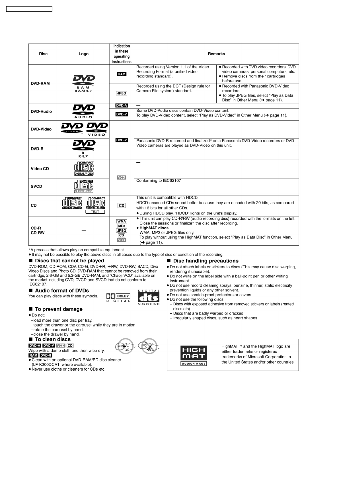
Disc played [8 cm or 12 cm]:
(1) DVD-RAM, (DVD-VR compatible, JPEG formatted discs)
(2) DVD-Audio
(3) DVD-Video
(4) DVD-R (DVD-Video compatible)
(5) CD-Audio (CD-DA)
(6) Video CD
(7) SVCD (Confirming to IEC62107)
(8) CD-R/CD-RW
(CD-DA, Video-CD, SVCD, MP3, WMA, JPEG formatted
discs)
(9) MP3/WMA*1
- Compatible compression rate:
MP3: between 32 kbps and 320 kbps
WMA: between 48 kbps and 320 kbps
(10) JPEG*1
- Exif Ver 2.1 JPEG Baseline files
- Picture resolution:
between 320 x 240 x and 6144 x 4096 pixels (Sub sampling is
4:2:2 or 4:2:0
(11) HighMAT Level 2 (Audio and Image)
Video output:
Output level: 1 Vp-p (75Ω)
Output terminal: Pin jack (1 system)
S-video output:
Y output level: 1 Vp-p (75Ω)
ORDER NO. MD0403064C3
DVD/CD Player
DVD-F87GCS
DVD-F87GN
Colour
(S)... Silver Type
C output level: NTSC; 0.286 Vp-p (75Ω)
PAL; 0.3000 Vp-p (75Ω)
Output connector: S terminal (1 system)
Component video output:
(NTSC: 480P/480I, PAL: 576I)
Y output level: 1 Vp-p (75Ω)
PBoutput level: 0.7 Vp-p (75Ω)
PRoutput level: 0.7 Vp-p (75Ω)
Output connector: Pin jack
(Y:green, P
Number of connectors: 1 system
udio output:
Output level: 2 Vrms (1kHz, 0dB)
Output connector: Pin jack
Number of connector: 5.1-channel discrete output (5.1
channel): 1 system
udio performance:
(1) Frequency response:
lDVD (linear audio):
lDVD audio:
lCD audio:
(2) S/N ratio:
lCD audio:
(3) Dynamic range:
lDVD (linear audio):
lCD audio:
(4) Total harmonic distortion:
lCD audio:
4 Hz-22 kHz (48 kHz sampling)
4 Hz-44 kHz (96 kHz sampling)
4 Hz-88 kHz (192 kHz sampling)
4 Hz-20 kHz
115 dB
100 dB
98 dB
0.0025%
:blue, PR:red)
B
© 2004 Panasonic AVC Networks Singapore Pte.
Ltd. All rights reserved. Unauthorized copying and
distribution is a violation of law.
Page 2
A
DVD-F87GCS / DVD-F87GN
Digital audio output:
Coaxial digital output: Pin Jack
Pickup:
Wavelength: 662 nm/ 785 nm
Laser power: CLASS 2/CLASS 3A
Power supply (For F87GN):AC 220 - 240 V, 50 Hz
Power supply (For F87GCS):AC 220 - 240 V, 50/60 Hz
Power consumption: 10 W
Dimensions: 430 (W) x 412.9 (D) x 68 (H) mm
Mass:
Power consumption in standby mode: approx. 0.7 W
Note:
1. Specifications are subject to change without notice.
Mass and dimensions are approximate.
pprox. 4.0kg
CONTENTS
Page Page
1 Before Use (For GCS Only)
2 Safety Precautions
2.1. General Guidelines
3 Before Repair and Adjustment
4 Prevention of Electro Static Discharge (ESD) to
Electrostatically Sensitive (ES) Devices
5 Handling the Lead-free Solder
5.1. About lead free solder (PbF)
6 Cautions to be taken when handling Optical Pickup
6.1. Handling Optical Pickup
6.2. Cautions to be taken during replacement of Optical Pickup
6.3. Grounding for Preventing Electrostatic Discharge
7 Precaution of Laser Diode
8 Accessories
9 Operation Procedure
10 Disc information
11 About HighMAT
11.1. What is HighMAT?
11.2. Why use HighMAT?
11.3. The advantages of using HighMAT
11.4. Outline of the HighMAT standard
12 Procedure for repairing the set
12.1. Distinguish the trouble cause
12.2. Diagnosis of Optical Pick-up Unit
13 Optical Pickup Self-Diagnosis and Replaceme nt Procedure
13.1. Self-diagnosis
13.2. Cautions to Be Taken During Replacement of Optical
Pickup and Spindle Motor
14 Self-Diagn osis Function
14.1. Automatic Displayed Error Codes
14.2. Memorized Error Codes
14.3. Service Mode Table 1
14.4. DVD/CD Self-Diagnosis Error Code Description
14.5. Error Codes Stored During No Play
14.6. Service Mode Table 2
14.7. Service Mode Table 3
14.8. Lock Function
4
4
4
4
5
5
5
6
6
6
6
7
8
9
10
13
13
13
13
14
16
17
19
21
21
22
23
23
23
23
24
24
25
26
27
14.9. Things to Do After Repair
15 Service precautions
15.1. Recovery after the player is repaired
15.2. DVD Player Firmware Version Upgrade Process
15.3. Firmware Version Upgrade Process by Using Recovery
Disc
16 Disassemb ly and Main Componen t Replacement Procedures
16.1. Disassembly flow chart
16.2. Printed Circuit Boards (P.C.B.) Position
16.3. Disassembling of Top Cabinet
16.4. Disassembling of DVD Lid
16.5. Disassembling of Front Panel
16.6. Disassembling of Rear Panel
16.7. Disassembling of Tray Assembly
16.8. Disassembly of Main P.C.B.
16.9. Disassembly of Tray Base Guide (L) and Tray Base Guide
(R)
16.10. Disassembly of Tray Base
16.11. Disassembly of Open Lock Gear
16.12. Disassembly of the Close Lock Gear & Close Lock Gear
Spring
16.13. Disassembly of the Tray Motor P.C.B. and Sensor P.C.B.
16.14. Disassembly of the CD Traverse Unit
16.15. Disassembly of the Pulley Gear
16.16. Disassembly of Loading Motor P.C.B.
16.17. Disassembly of Drive Gear (A) & (B)
16.18. Disassembly of Magnet Holder washer, Magnet and
Clamper
16.19. Disassembly of Cam Gear & Support Piece
16.20. Disassembly of Slide Plate (L) & (R) and Change Lever
16.21. Assembly of Tray Base
17 Service Position
17.1. Checking Procedure
17.2. Checking the Main P.C.B. , Panel P.C.B, Selection Panel
P.C.B. and Display Panel P.C.B.
18 Adjustmen t Procedures
27
28
28
28
28
30
30
31
32
32
32
33
33
33
34
34
34
35
35
35
36
36
36
37
37
37
38
39
39
39
40
2
Page 3

DVD-F87GCS / DVD-F87GN
18.1. Service Tools and Equipment 40
19 Illustration of IC 痴, Transistors and Diodes
20 Block Diagram
21 Schematic Diagram
21.1. (A) Optical Pickup Unit Circuit
21.2. (A) DVD Module (In/Out) Circuit
21.3. (A) DVD Module (DV2) Circuit
21.4. (B) Main (Operation Control) Circuit
21.5. (B) Main (Audio- out 1) Circuit
21.6. (B) Main (Audio- out 2) Circuit
21.7. (B) Main (Video Out) Circuit
21.8. (B) Main (Power) Circuit
21.9. (C) Panel Circuit, (D) Display Panel Circuit & (E) Selection
Panel Circuit
21.10. (F) Sensor Circuit, (G) Tray Motor Circuit & (H) Loading
42
22 Printed Circuit Board
43
49
50
51
54
58
60
62
23 Wiring Connection Diagram
24 Parts Location and Replacement Parts List
63
64
Motor Circuit
22.1. (A) DVD Module P.C.B. (Side: A & B)
22.2. (B) Main P.C.B.
22.3. (C) Panel P.C.B., (D) Display Panel P.C.B. & (E) Selection
Panel P.C.B.
22.4. (F) Sensor P.C.B., (G) Tray Motor P.C.B. & (H) Loading
Motor P.C.B.
24.1. Loading Mechanism, Traverse Unit and Cabinet
24.2. Component Parts List
66
24.3. Packing Materials & Accessories Parts List
24.4. Packaging
68
69
69
71
73
75
76
78
79
82
87
88
3
Page 4
DVD-F87GCS / DVD-F87GN
1 Before Use (For GCS Only)
Be sure to disconnect the mains cord before adjusting the voltage selector.
Use a minus(-) screwdriver to set the voltage selector (on the rear panel) to the voltage setting for the area in which the unit will
be used. (If the power supply in your area is 117V or 120V, set to the “127V” position.)
Note that this unit will be seriously damaged if this setting is not made correctly. (There is no voltage selector for some countries,
the correct voltage is already set.)
2 Safety Precautions
2.1. General Guidelines
1. When servicing, observe the original lead dress. If a short circuit is found, replace all parts which have been overheated or
damaged by the short circuit.
2. After servicing, see to it that all the protective devices such as insulation barriers, insulation papers shields are properly
installed.
3. After servicing, make the following leakage current checks to prevent the customer from being exposed to shock hazards.
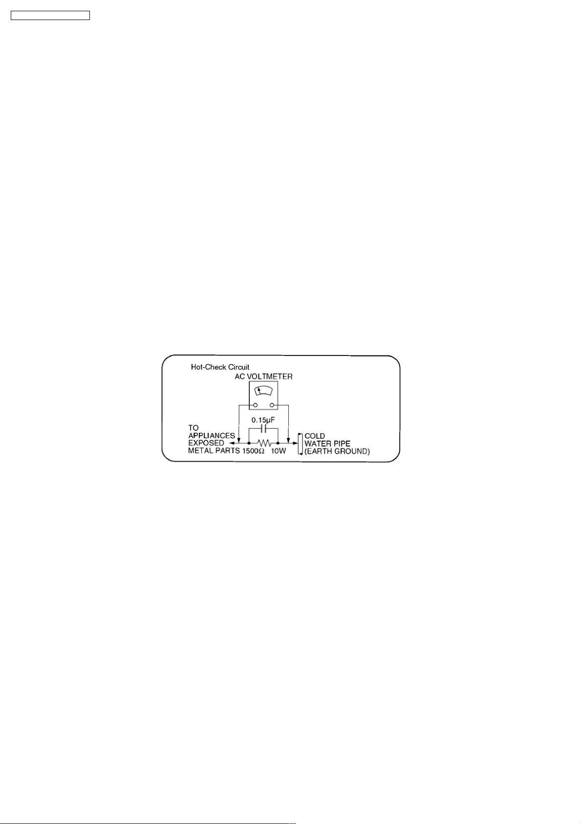
2.1.1. Leakage Current Cold Check
1. Unplug the AC cord and connect a jumper between the two prongs on the plug.
2. Measure the resistance value, with an ohmmeter, between the jumpered AC plug and each exposed metallic cabinet part on
the equipment such as screwheads, connectors, control shafts, etc. When the exposed metallic part has a return path to the
chassis, the reading should be between 1MΩand 5.2MΩ.
When the exposed metal does not have a return path to the chassis, the reading must be・.
Figure 1
2.1.2. Leakage Current Hot Check
(See Figure 1)
1. Plug the AC cord directly into the AC outlet. Do not use an isolation transformer for this check.
2. Connect a 1.5kΩ, 10 watts resistor, in parallel with a
good earth ground such as a water pipe, as shown in Figure 1.
3. Use an AC voltmeter, with 1000 phms/volt or more sensitivity, to measure the potential across the resistor.
4. Check each exposed metallic part, and measure the voltage at each point.
5. Reverse the AC plug in the AC outlet and repeat each of the above measurements.
6. The potential at any point should not exceed 0.75 volts RMS. A leakage current tester (Simpson Model 229 or equivalent) may
be used to make the hot checks, leakage current must not exceed 1/2 milliamp. In case a measurement is out of the limits
specified, there is a possibility of a shock hazard, and the equipment should be repaired and rechecked before it is returned to
the customer.
0.15µF capacitor, between each exposed metallic part on the set and a
3 Before Repair and Adjustment
Disconnect AC power, discharge Power Supply Capacitors C1011 , C1041 & C1083 through a 10 Ω, 5W resistor to ground.
DO NOT SHORT-CIRCUIT DIRECTLY (with a screwdriver blade, for instance), as this may destroy solid state devices.
After repairs are completed, restore power gradually using a variac, to avoid overcurrent.
Current consumption at AC 120V, 60Hz in NO SIGNAL mode should be ~215 mA .
4
Page 5
DVD-F87GCS / DVD-F87GN
4 Prevention of Electro Static Discharge (ESD) to
Electrostatically Sensitive (ES) Devices
Some semiconductor (solid state) devices can be damaged easily by electricity. Such components commonly are called
Electrostatically Sensitive (ES) Devices. Examples of typical ES devices are integrated circuits and some field-effect transistors and
semiconductor “chip” components. The following techniques should be used to help reduce the incidence of component damage
caused by electro static discharge (ESD).
1. Immediately before handling any semiconductor component or semiconductor-equiped assembly, drain off any ESD on your
body by touching a known earth ground. Alternatively, obtain and wear a commercially available discharging ESD wrist strap,
which should be removed for potential shock reasons prior to applying power to the unit under test.
2. After removing an electrical assembly equiped with ES devices, place the assembly on a conductive surface such as aluminium
foil, to prevent electrostatic charge build up or exposure of the assembly.
3. Use only a grounded-tip soldering iron to solder or unsolder ES devices.
4. Use only an anti-static solder remover device. Some solder removal devices not classified as “anti-static (ESD protected)” can
generate electrical charge to damage ES devices.
5. Do not use freon-propelled chemicals. These can generate electrical charges sufficient to damage ES devices.
6. Do not remove a replacement ES device from its protective package until immediately before you are ready to install it. (Most
replacement ES devices are packaged with leads electrically shorted together by conductive foam, aluminium foil or
comparable conductive material).
7. Immediately before removing the protective material from the leads of a replacement ES device, touch the protective material
to the chassis or circuit assembly into which the device will be installed.
Caution
Be sure no power is applied to the chassis or circuit, and observe all other safety precautions.
8. Minimize bodily motions when handling unpackaged replacement ES devices. (Otherwise harmless motion such as the
brushing together of your clothes fabric or the lifting of your foot from a carpeted floor can generate static electricity (ESD)
sufficient to damage an ES device).
5 Handling the Lead-free Solder
5.1. About lead free solder (PbF)
Distinction of PbF P.C.B.:
P.C.B.s (manufactured) using lead free solder will have a PbF stamp on the P.C.B.
Caution:
· Pb free solder has a higher melting point than standard solder; Typically the melting point is 50 - 70°F (30 - 40°C) higher. Please
use a high temperature soldering iron. In case of soldering iron with temperature control, please set it to 700 ± 20°F (370 ±
10°C).
· Pb free solder will tend to splash when heated too high (about 1100°F/600°C).
· When soldering or unsoldering, please completely remove all of the solder on the pins or solder area, and be sure to heat the
soldering points with the Pb free solder until it melts enough.
5
Page 6
DVD-F87GCS / DVD-F87GN
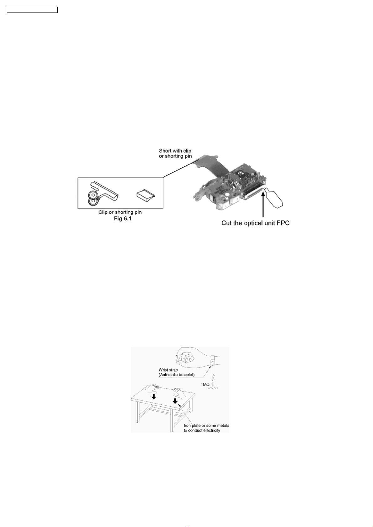
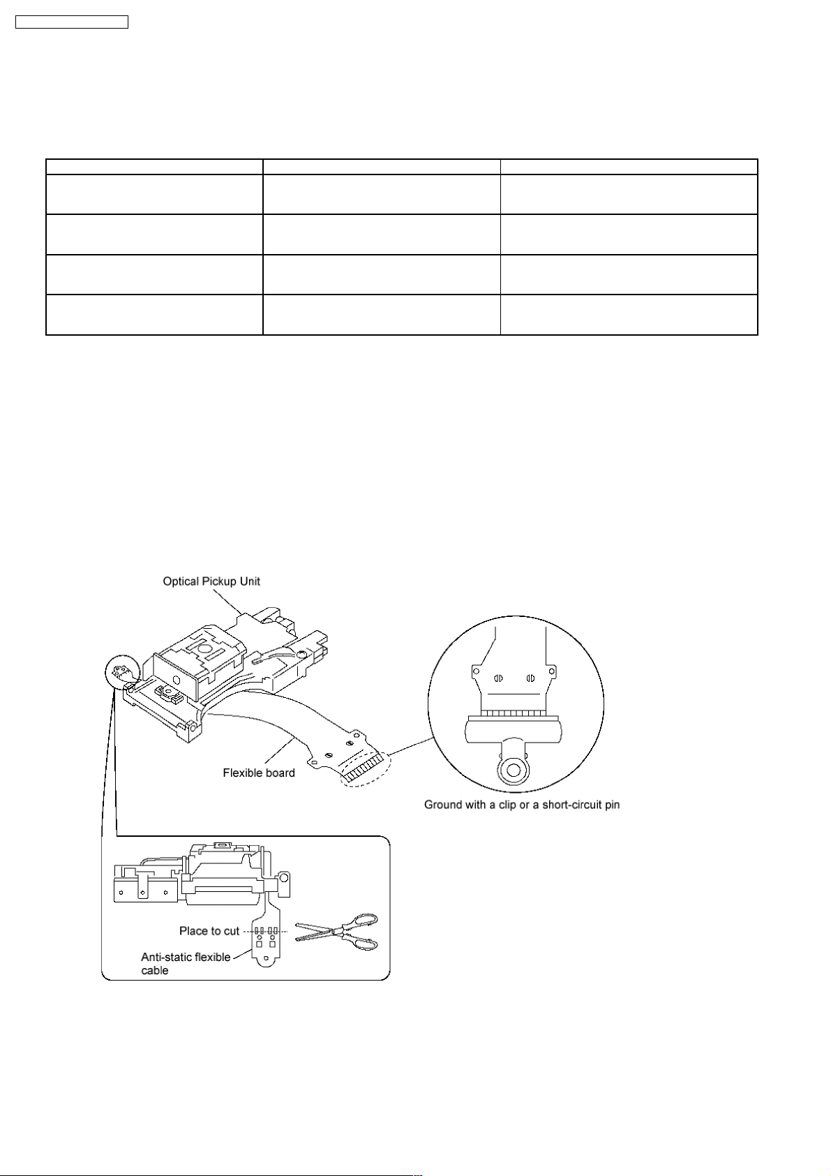
6 Cautions to be taken when handling Optical Pickup
The laser diode used inside optical pickup could be destroyed due to static electricity as a potential difference is caused by
electrostatic load discharged from clothes or human body. Handling the parts carefully to avoid electrostatic destruction during
repair.
6.1. Handling Optical Pickup
1. Do not impact on optical pickup as the unit structurally uses an extremely precise technology.
2. Short-circuit the flexible cable of optical pickup remove from the circuit board using a short-circuit pin or clip in order to prevent
laser diode from electrostatic destruction (Refer to Fig. 6.1 and Fig. 6.2)
3. Do not handle flexible cables forcibly as this may cause snapping. Handle the parts carefully (Refer to Fig. 6.1)
4. A new optical pickup is equipped with an anti-static flexible cable. After replacing and connecting to the flexible board, cut the
anti-static flexible cable. (Refer to Fig. 6.1)
6.2. Cautions to be taken during replacement of Optical Pickup
Supplied optical pickup is equipped with a short clip found its flexible cable in order to prevent electrostatic destruction of laser
diode. Before connection, remove the short clip, and check that the short land is opened. (Remove solder if the part is short-circuit).
6.3. Grounding for Preventing Electrostatic Discharge
1. Human body grounding
Use the anti-static wrist strap to discharge the static electricity accumulated in your body. (Refer to Fig. 6.2)
2. Work place grounding
Place a conductive material (conductive sheet) or ironboard where optical pickup is placed. (Refer to Fig. 6.2)
Note :
Keep your clothes away from optical pickup as wrist strap does not release the static electricity charged in clothes.
Fig. 6.2
6
Page 7
DVD-F87GCS / DVD-F87GN
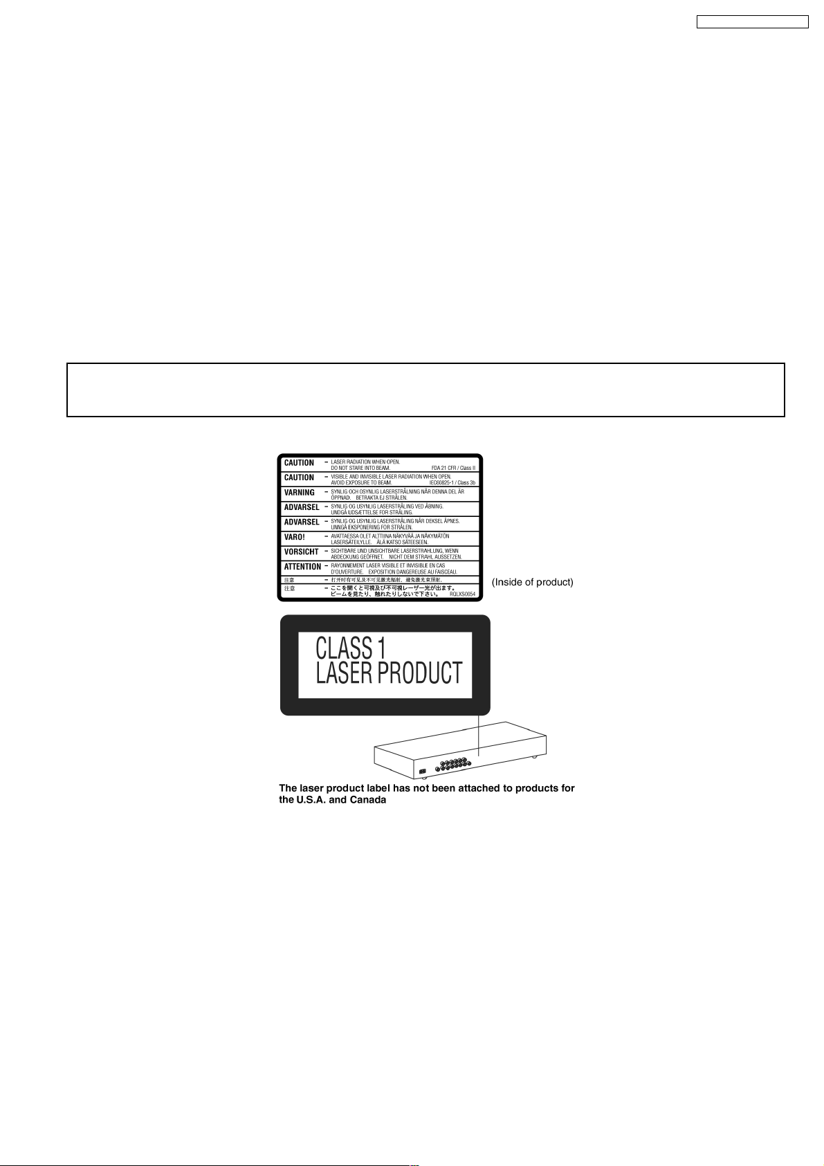
7 Precaution of Laser Diode
CAUTION :
This unit utilizes a class 1 laser.
Invisible laser radiation is emitted from the optical pickup lens.
Wavelength: 665nm/790nm.
Maximum output radiation power from pickup: 100µW/VDE
When the unit is turned on :
1. Do not look directly into the pick up lens.
2. Do not use optical instruments to look at the pick up lens.
3. Do not adjust the preset variable resistor on the pickup lens.
4. Do not disassemble the optical pick up unit.
5. If the optical pick up is replaced, use the manufacturer’s specified replacement pick up only.
6. Use of control or adjustments or performance of procedures other than those specified herein may result in hazardous
radiation exposure.
CAUTION!
THIS PRODUCT UTILIZES A LASER.
USE OF CONTROLS OR ADJUSTMENTS OR PERFORMANCE OF PROCEDURES OTHER THAN THOSE SPECIFIED HEREIN MAY RESULT
IN HAZARDOUS RADIATION EXPOSURE.
n Use of Caution Labels
7
Page 8
DVD-F87GCS / DVD-F87GN
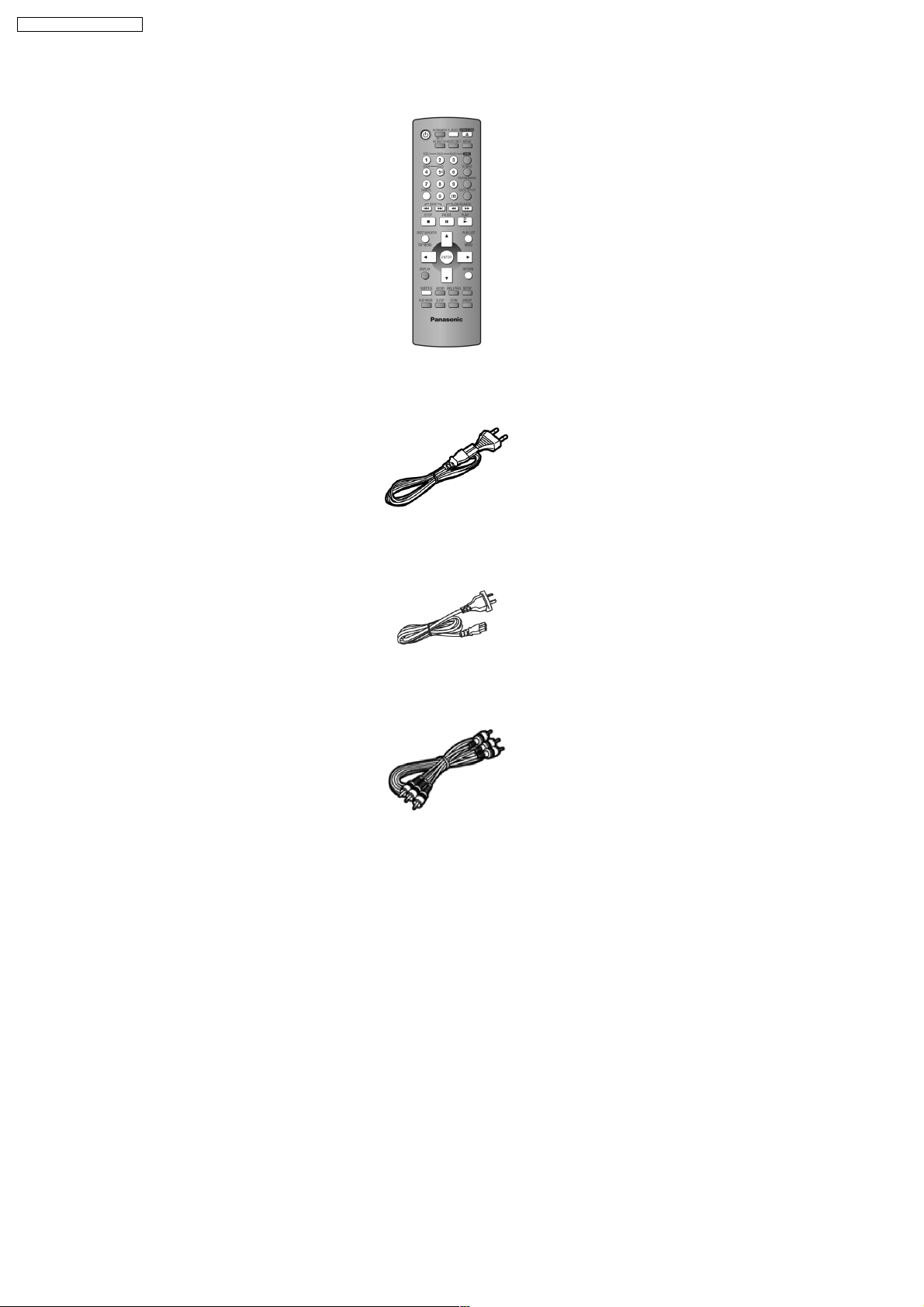
8 Accessories
Remote
control
AC power supply cord
(for GCS)
AC power supply
cord (for GN only)
Audio/video Cable
8
Page 9
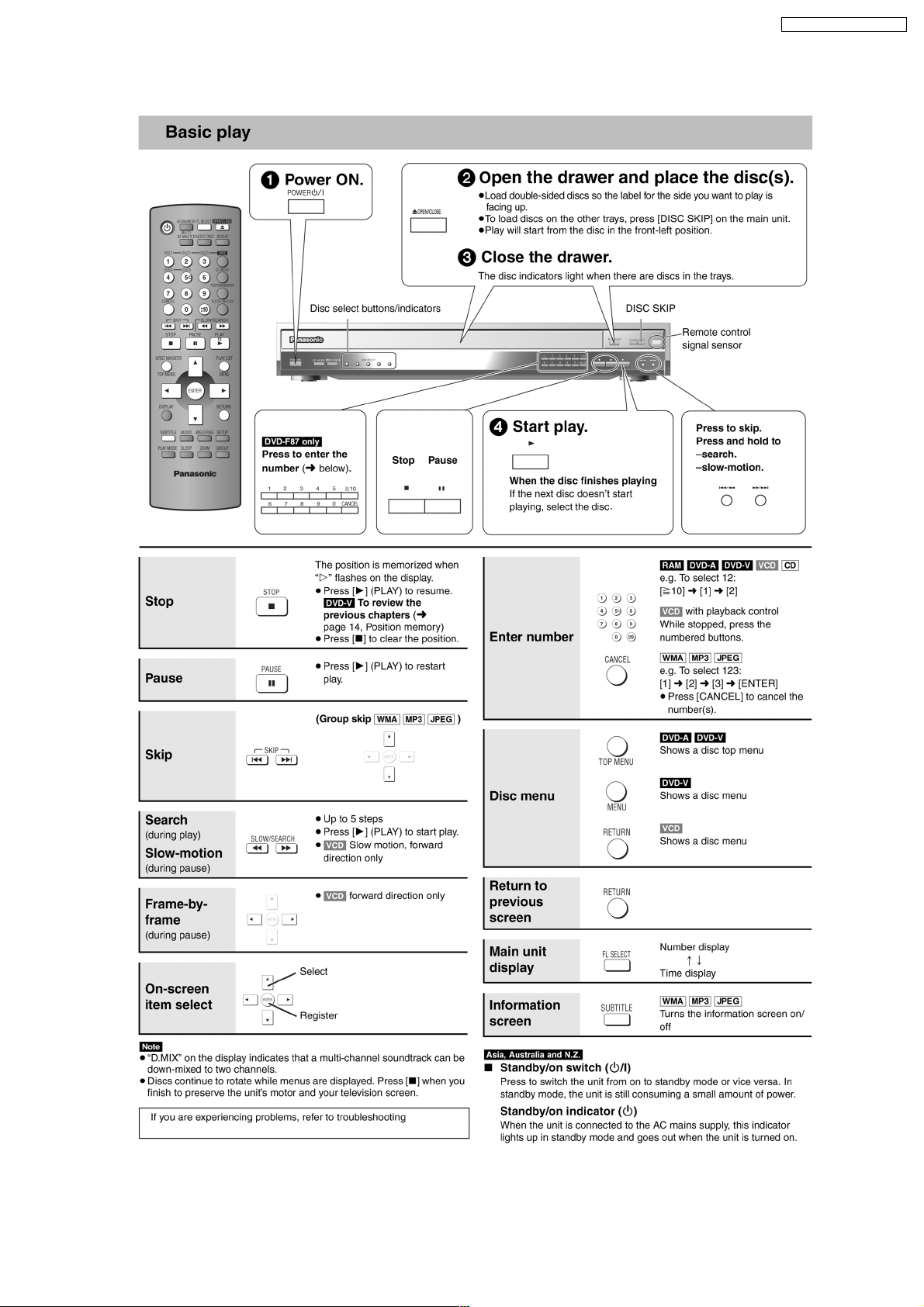
9 Operation Procedure
DVD-F87GCS / DVD-F87GN
9
Page 10
DVD-F87GCS / DVD-F87GN
10 Disc informatio n
10
Page 11
DVD-F87GCS / DVD-F87GN
11
Page 12
DVD-F87GCS / DVD-F87GN
12
Page 13
DVD-F87GCS / DVD-F87GN
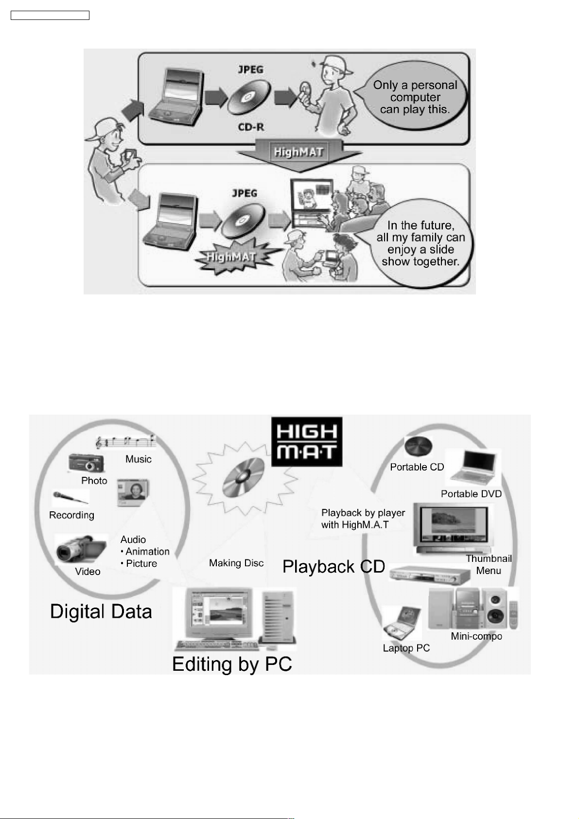
11 About HighMAT
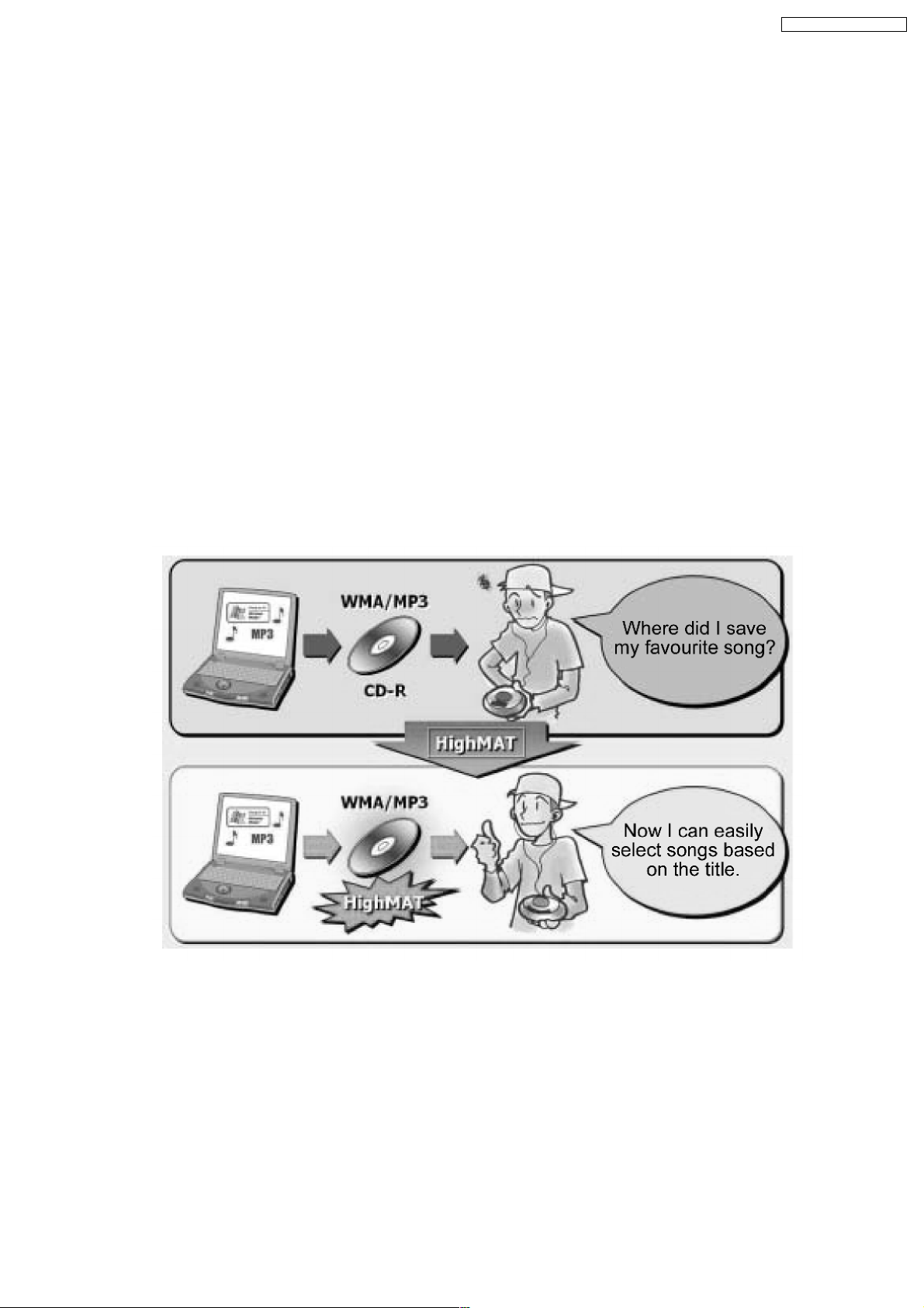
11.1. What is HighMAT?
This word combines the abbreviations of Matsushita Electric Industrial Co. Ltd. and High Performance Media Access Technology,
and is a trademark of Microsoft Corporation. The products with the HighMAT logo shown below are made according to the
HighMAT standard.
HighMAT is a format that allows users to save digital contents such as photographs, audio, and images on a CD. This gives
consistency in the way of reading data when general consumer products (such as DVD players) and PCs are used, and thus, it is
easy to operate for the user.
11.2. Why use HighMAT?
Up to now, there was no harmonized standard from playing digital content stored in CD-ROM formats (including CD-R) on
consumer products like DVD players.Therefore, we used to have problems such as follow:
· There was no common play list or attached information on contents, which is called metadata.
· The data compression method differed according to the equipment.
· As the number of CD-ROMs recorded increased retrieved the contents became more difficult.
· Because display and operation methods were different depending on the equipment, the play order of the content on the same
disc could change.
11.3. The advantages of using HighMAT
Applying the HighMAT standard will solve the following problems and will improve usability.
· It will create a common user interface for both PC and consumer products.
· Regardless of the types of consumer products, such as DVD players, portable CD players, car stereos, and micro computers,
a consistent way to pay for digital content will be created and it will make it easier to retrieve data.
13
Page 14
DVD-F87GCS / DVD-F87GN
· You can also play digital content on the disc, which was created in accordance with the HighMAT format with a conventional
CD-ROM player.
11.4. Outline of the HighMAT standard
1. Recording medium
· CD-R/CD-RW
· Supports ISO 9660 Level Expanded Joliet
· For multiple session
2. Support data format
· Level 1 player: WMA, MP3 (MPEG-1 Audio Layer 3)
· Level 2 player: WMA, MP3 (MPEG-1 Audio Layer 3), JPEG
· Level 3 player: WMA, MP3 (MPEG-1 Audio Layer 3), JPEG, WMV, MPEG4 (optional)
3. Limitation of data format
14
Page 15

DVD-F87GCS / DVD-F87GN
· WMA, MP3 (MPEG-1 Audio Layer 3) 64 kbps - 160.999 kbps, 44.1 KHz, stereo, fixed bit rate/ variable bit rate.
· WMA, V2 and above, excluding Lossless/Voice/Pro
· JPEG: Max 6M pixel, Maximum file size: 3 MB
4. Limitations regarding the number of files on the media, etc.
· Total number of audio files: Maximum 450
· Total number of still picture files: Maximum 999
· Total number of animation files: Maximum 200
· Total number of directories: Maximum 400
· Length of a file name: Maximum 108 characters (Unicode)
· Total number of play lists: Maximum 200
· Number of contents in the playlist: Maximum 900
5. Composition of HighMAT disc
· Menu: Classified for the navigation of the HighMAT digital contents. When menu selected, its submenu or the play list will
be displayed.
· Play list: A list in which one or more digital contents are arranged in order
· Group: Sub-divided group of a play list.
· Digital Contents: Audio, still picture, and animation data.
15
Page 16
DVD-F87GCS / DVD-F87GN
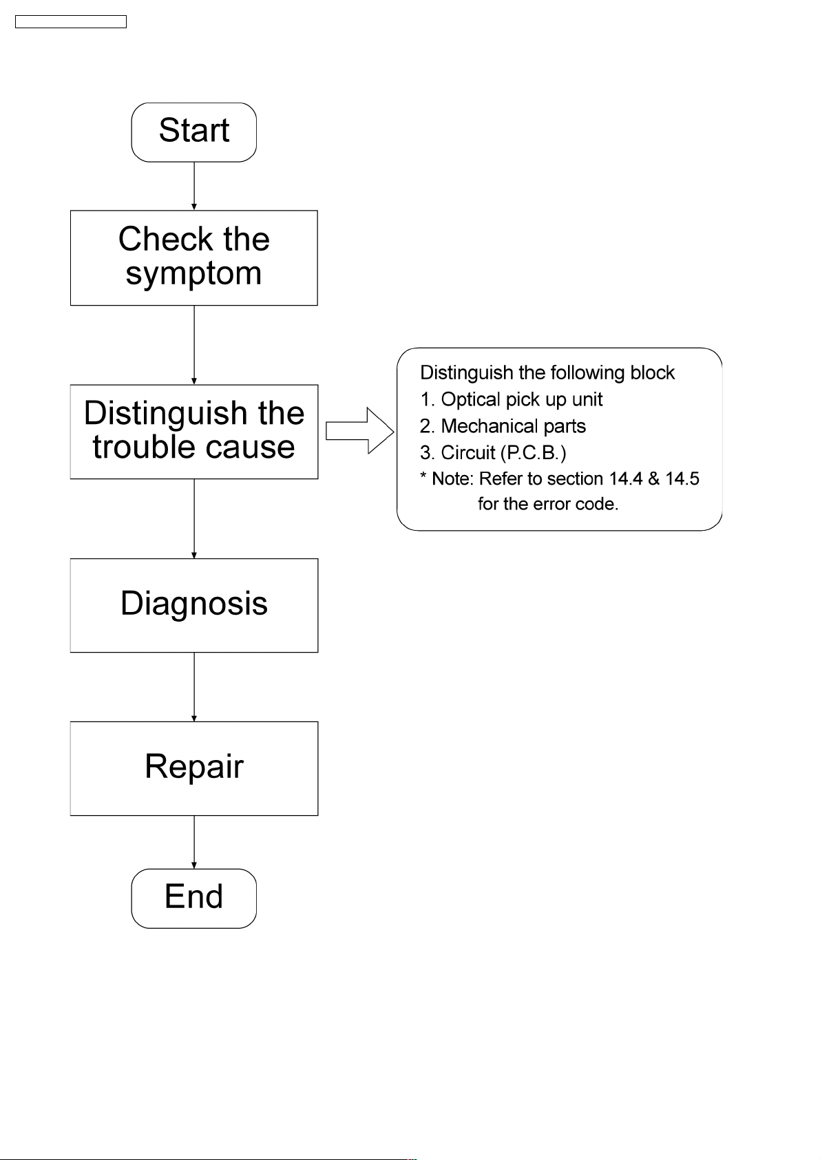
12 Procedure for repairing the set
16
Page 17
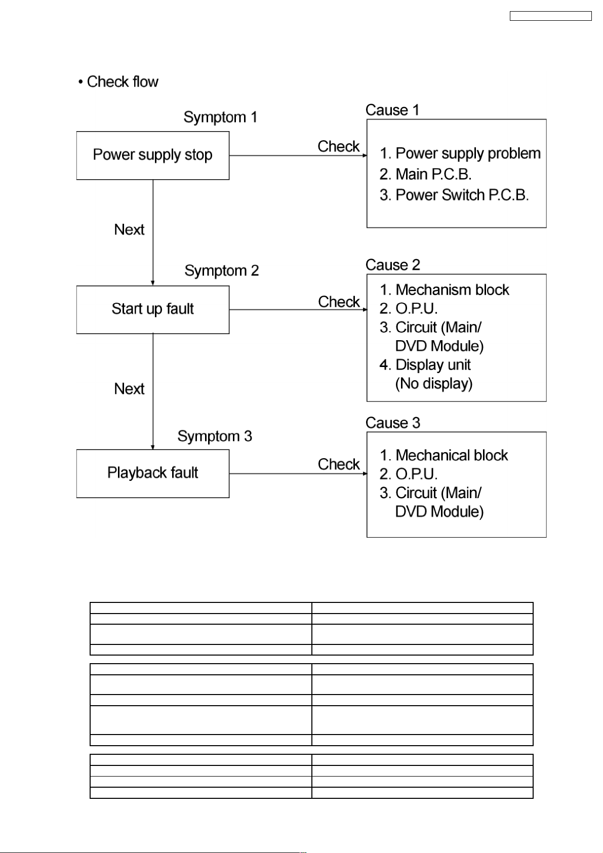
12.1. Distinguish the trouble cause
DVD-F87GCS / DVD-F87GN
How to distinguish the trouble
1. View mechanism part if visual damage occurred.
Confirm the movement of mechanism parts assembly
(tray ass’y, loading mechanism ass’y, etc.).
Cause 1 Possible fault
1. Power supply problem Power switch (S6611), AC inlet (P1001)
2. Main P.C.B. D1002, D1011, F1001, IC1021, L1001, Q1051, T1021,
3. Power Switch P.C.B. CPU (IC6001), X6001, IC6061, IC6062
Cause 2 Possible fault
1. Mechanism block Tray and loading mechanical block, traverse unit, CPU
2. O.P.U. Refer to the diagnosis of OPU
3. Circuit LD drive, servo (Traverse, Focus, Tracking unit), IC8271 &
4. Display Unit (No display) FL (DP6501) unit, IC6501 (CPU), Pin 1 to 4 (FP6501)
Cause 3 Possible fault
1. Mechanical block Traverse block (Tilt adjustment)
2. O.P.U. Refer to the diagnosis of OPU
3. Circuit Servo (Focus, tracking) IC8271, Motor Drive (IC8251)
2. Diagnose if Optical Pickup Unit is faulty (refer to
diagnosis of Optical Pickup Unit).
3. If mechanism and OPU are OK, it is P.C.B.
IC1101
(IC6001)
IC8251
Disc sensor (Pin 124, 126) of IC8001)
17
Page 18

DVD-F87GCS / DVD-F87GN
4. Main CCT Audio signal processing (IC4310, IC4302, IC4303 & IC4304)
5. DVD Module CCT Audio signal processing (IC8451) - pin 13, 14, 9, 10, 11, 12
Cause 3 Possible fault
Video signal processing (IC3501) - pin 31, 25, 22, 19
Video signal processing (IC8001)
18
Page 19
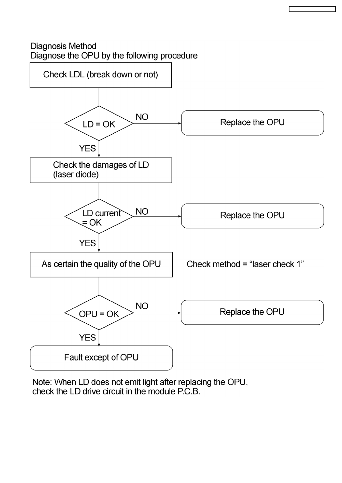
12.2. Diagnosis of Optical Pick-up Unit
DVD-F87GCS / DVD-F87GN
How to distinguish Laser destruction/damage
Confirmation 1
Remove cover of mechanism block so that you will see the lens of optical pickup.
Confirm emission of laser at the moment when power switch is turned on.
If there is no laser emission, laser diode is faulty.
Confirmation 2
19
Page 20

DVD-F87GCS / DVD-F87GN
While holding “Pause” and “Open/Close” button, press “Display” button on the remote controller. Unit display laser current on
FL.
From the reading of display, you can judge if laser diode is damaged or not.
Reading on the right side should be less than 70. If reading is more than 70, laser is damaged.
How to confirm if Optical Pickup is OK
Confirmation 1
1. Confirmation of jitter value with test disc. (Refer below for how to check jitter)
2. Lens cleaning.
3. Reconfirm jitter value.
4. Perform tile adjustment. (Refer to tilt adjustment)
5. Reconfirm jitter value. (To confirm jitter value, while pressing “Pause” and “Open/Close” button, press numeric “5” on remote
controller.)
Unit display jitter value on FL.
Confirmation 2
If servo is very unstable due to optical error and you cannot confirm jitter value, clean the lens and check appearance of pick
up unit (cutting coil of actuator, etc), then check circuitry.
20
Page 21
DVD-F87GCS / DVD-F87GN
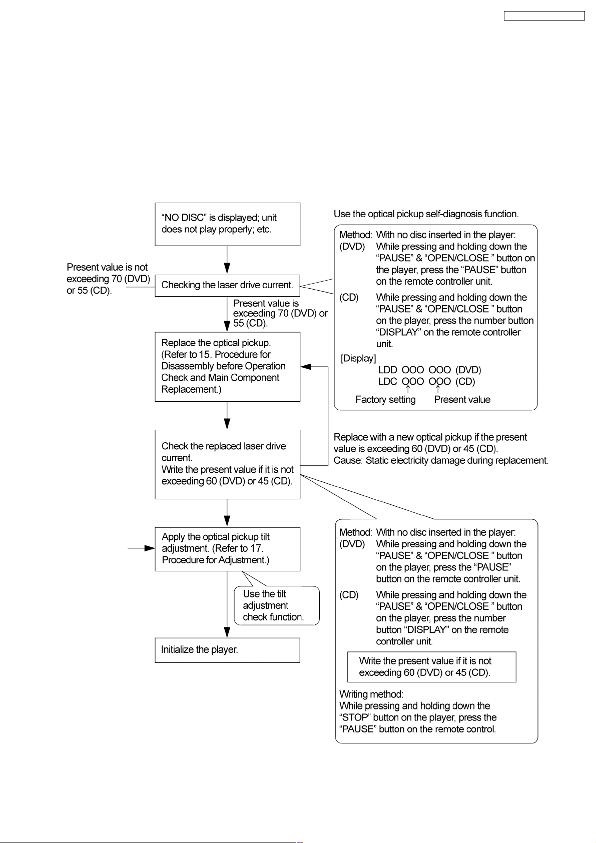
13 Optical Pickup Self-Diagn osis and Replacem ent
Procedure
13.1. Self-diagnosis
This unit is equipped with the optical pickup self-diagnosis function and the tilt adjustment check function. Follow the procedure
described below during repair in order to perform self-diagnosis and tilt adjustment effectively. Especially when “NO DISC” is
displayed, be sure to apply the self-diagnosis function before replacing with an optical pickup. Replacement of optical pickup
generally requires when the present value of laser drive exceeds 70 (DVD) or 55 (CD).
Note:
Start diagnosis within three minutes after turning on the power (as diagnosis fails when the unit becomes warm).
21
Page 22
DVD-F87GCS / DVD-F87GN
13.2. Cautions to Be Taken During Replacement of Optical Pickup and
Spindle Motor
Before replacing the optical pickup and spindle motor, check for the total usage time respectively. Follow the checking method
described below.
Item Player mode and button combination Display
Checking DVD, CD laser usage time In STOP mode, press PAUSE and FWD-SKIP
Checking spindle motor usage time While displaying Timer 1 data, press STOP and
Resetting DVD, CD laser usage time In STOP mode, press PAUSE and FWD-SKIP
Resetting spindle motor usage time Whiledisplaying Timer 2 data, press STOP and
buttons on the player, and “5” button on the
remote control unit.
FWD-SKIP buttons on the player, and “5”
button on the remote control unit.
buttons on the player, and “6” button on the
remote control uit.
FWD-SKIP buttons on the player and “6” button
on the remote control unit.
13.2.1. Cautions to be taken during replacement of optical pickup
Optical pickup could be damaged due to the static electricity discharged from human body. Wear proper protection gear against
static electricity during optical pickup and its peripheral repair. (Refer to “Cautions to Be Taken When Handling Optical Pickup”.)
· Do not touch laser diode, actuator and their peripherals.
· Do not check laser diode with a tester and such. (The tester will be destroyed.)
· For short-circuiting or removing laser diode, the use of an anti-static soldering iron is recommended. (Recommended model:
HAKKO ESD product)
· Solder the land of the flexible cable in the optical pickup.
Note:
If an anti-static soldering iron is not available, short-circuit the terminal surface of the flexible cable and then the land using a
clip or equivalent device.
T1_xxxx_yyyy
xxxx(DVD), yyyy(CD): total time is displayed with a
four-digit number by the ten hours.
T2_xxxx
xxxx: total time is displayed with a four-digit number
by the ten hours.
T1_0000_0000
T2_0000
22
Page 23
DVD-F87GCS / DVD-F87GN
14 Self-Diagnosis Function
This unit is equipped with the self-diagnosis function, which displays an error when it occurs, for use during servicing.
14.1. Automatic Displayed Error Codes
14.1.1. Automatic Display Function
For a power unit error, the code is automatically displayed.
F61: Automatically displayed on the LCD of the player.
14.1.2. Re-Display
· For F61 Display
−
− When the code, F61 is displayed, the power is automatically turned off.
− −
−
− The code, F61 is displayed for three seconds, and then the current time appears.
− −
−
− To retrieve the code, turn on the power button so that the code F61 appears, however, is switched to time display after three
− −
seconds, and the power is automatically turned off.
14.1.3. Description of Error Code
14.1.3.1. F61
· State, Condition
When the power is turned on, the unit is automatically turned off. The power does not turn on.
· Cause, Troubleshooting
Power circuit system failure and/or direct current flown to speaker terminal.
Identify the cause and replace with new parts.
14.2. Memorized Error Codes
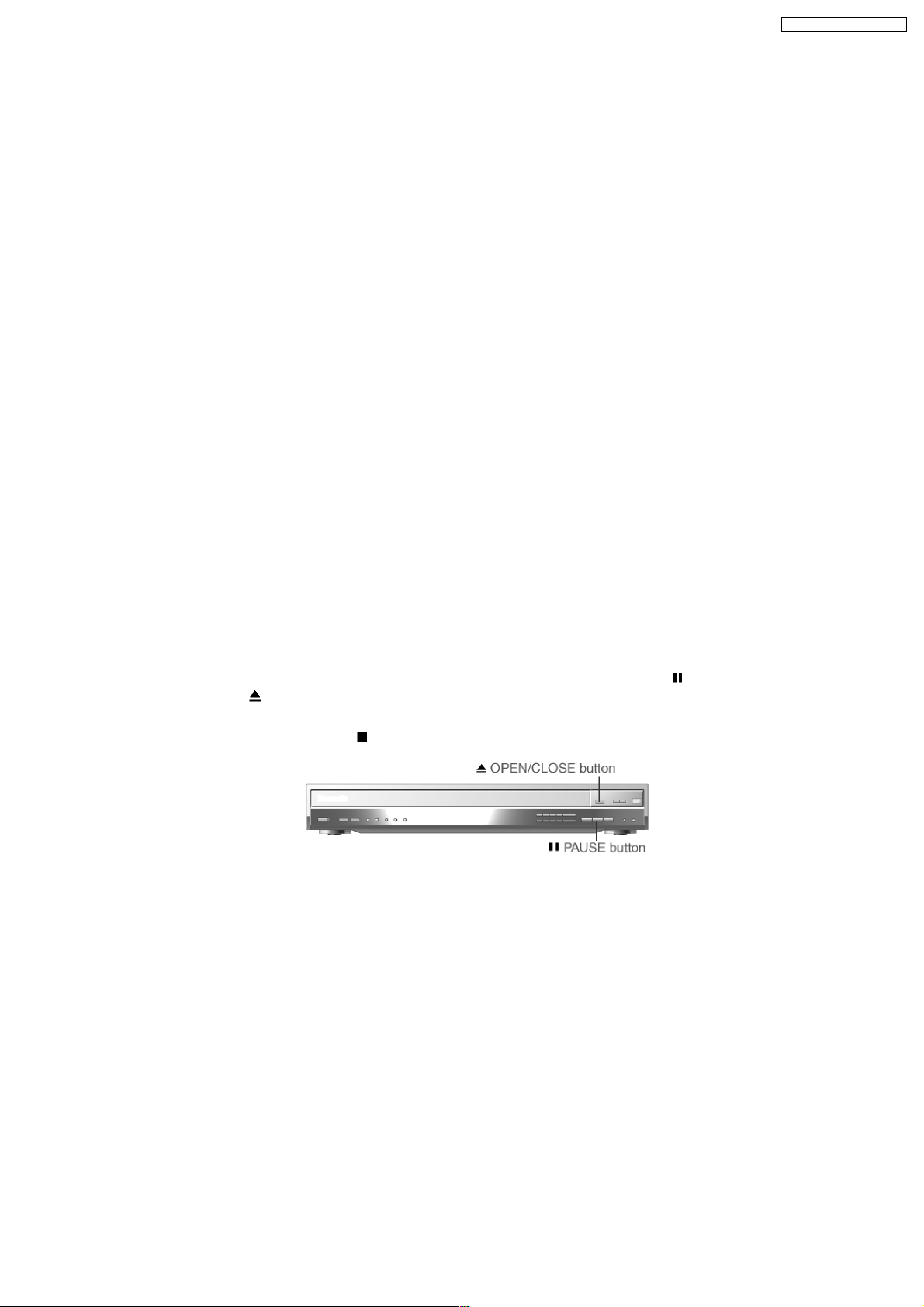
14.2.1. Activating Self-Diagnosis Function and Displaying Method
1. Turn on the power.
2. Select DVD/CD function. With no DVD/CD inserted in the player, press and hold down the
seconds, and press the
3. Press the ”0” button on remote control. If a memorized error is detected, the result of self diagnosis is displayed.
If several errors are detected, press the
OPEN/CLOSE button for at least two seconds in order to display “F_ _ _”.
button to display each.
Fig. 13-1
14.2.2. Re-Display
PAUSE button for at least two
· Press the power button to turn off the power, and then turn on the power.
· The details of self diagnosis are stored in the unit memory.
To retrieve them, follow the procedure described the above, “Activating Self-Diagnosis Function and Displaying Method”.
14.3. Service Mode Table 1
The service modes can be activated by pressing various button combination on the player and the remote control unit.
23
Page 24
DVD-F87GCS / DVD-F87GN
Player buttons Remote control unit buttons Application
PAUSE +
OPEN/CLOSE
PAUSE
SKIP/SEARCH<<
OPEN/CLOSE
PAUSE
0 Displaying the UHF display F _ _ _
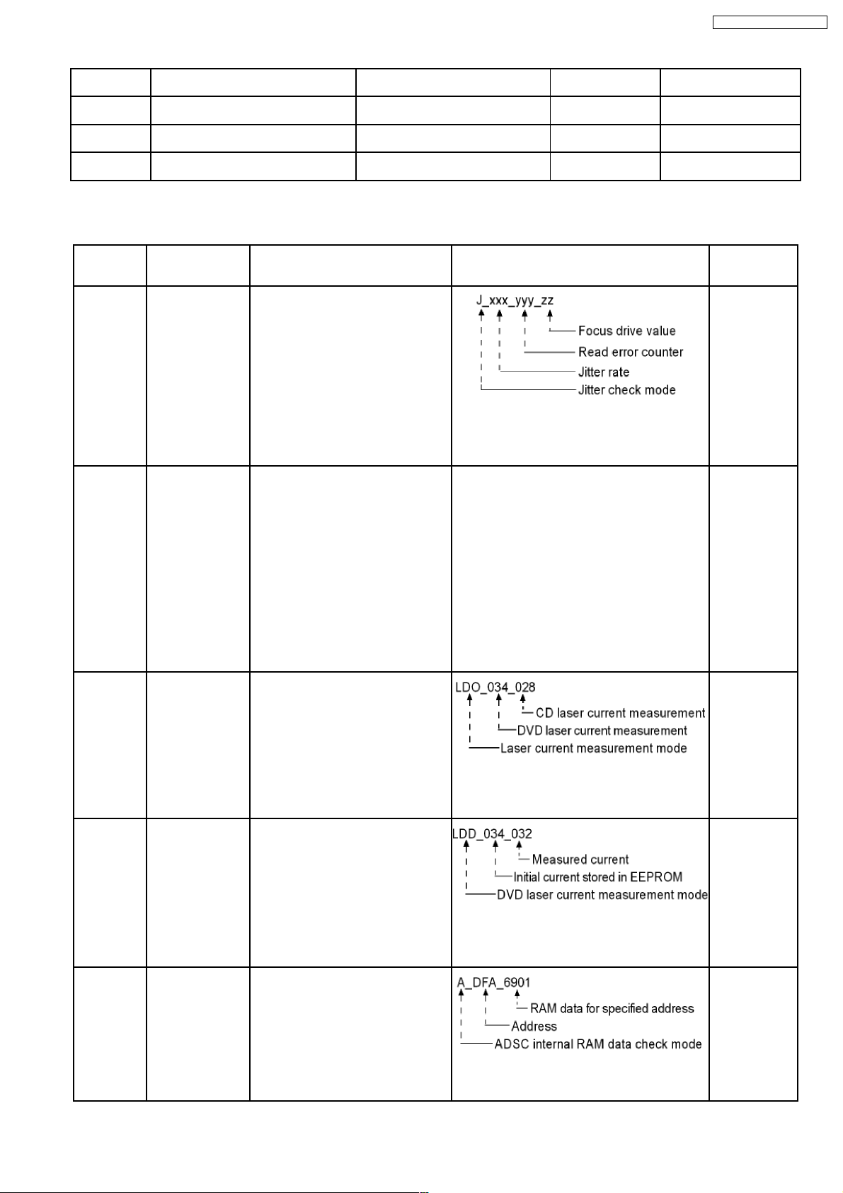
5 Jitter check, tilt adjustment
*Display show J_xxx_yyy_zz
“yyy” and “zz” shown to the right have nothing to do with
the jitter value. “yyy” is the error counter, while “zz” is the
focus drive value.
Refer to Section 16.1.4 for Optical Adjustment (Optical
Pickup Tilt Adjustment)
6 Checking the region numbers and broadcast system
7 Checking the program version
9 Lighting Confirmation Function of Display Tube
DISPLAY Checking the laser drive current
PAUSE Writing the laser drive current value after replacing the
optical pickup (do not use for anything other than optical
pickup replacement)
Initializing the DVD player
(restoring factory preset settings)
*Use when replacing a microprocessor, microprocessor
peripheral, or P.C.B.
14.4. DVD/CD Self-Diagnosis Error Code Description
Error Code State, Conditon Cause, Troubleshooting
H15 The disc tray cannot be opened: it closes spontaneously. Disc tray open/close detection switch (S1001) failure.
H16 The disc tray cannot be closed: it opens spontaneously.
(Check and replace)
Error Code Meaning Details
U.H.Error
U11 Focus servo failure
H01 Tray loading failure
H02 Spindle servo failure (Spindle servo, DSC, SP motor, CLV servo failure)
H03 Traverse motor failure
H04 Tracking servo error
H05 Seek timeout failure
H06 Power supply error
DSC system
F500 DSC failure DSC stops due to servo failure.
F501 DSC not Ready failure Communication failure between DSC and system computer
F502 DSC Time out failure See F500.
F503 DSC communication failure Communication failure (Result failure occurs after communication
F505 DSC Attention Error See F500.
F506 Invalid media Disc is placed upside down; TOC is unreadable or invalid disc is
Disc Code
F103 Ilegal highlight position Disc standard is possibly illegal when highlight is displayed.
IIC Error
F4FF Forced initialization failure (Time out)
F880 Unsuitable task number When a message arrives from not existing task
F890 A message is sent during AV task transmission During transmission of a message to AV task
F891 Unable to transmit a message to AV task When transmission of a message to AV task starts
F893 DVD module problem Firmware version
F894 EEPROM failure
F8A0 Unsuitable message command When transmission of a message to AV task starts
F897 Main unit not initialized properly When power-up, (Do initialization of main unit)
(Startup, focus failure, etc.)
(No communication because DSC does not move)
command is transmitted.)
inserted.
14.5. Error Codes Stored During No Play
Error Code Meaning System Computer Item Setting Task Internal error in system
F0BF 6) Unable to replay due to physical layer
identification failure
F0C0 8) DVD: Unable to replay due to no DVD
Video/Audio/VR
F0C1 9) DVD: Prohibited due to illegal
regional code
F0C2 A) DVD: No replay due to PAL system PCND_NOPLAY_PAL 0x90 DiscManager 0xD0C2
PCND_NOPLAY_PHYSICAL 0x50 DriveManager 0xD0BF
PCND_NOPLAY_VIDEO 0x70 DiscManager 0xD0C0
PCND_NOPLAY_RCD 0x80 DiscManager 0xD0C1
24
computer
Page 25
DVD-F87GCS / DVD-F87GN
Error Code Meaning System Computer Item Setting Task Internal error in system
F0C3 B) DVD: All title replay prohibited in
parental setting
F0C4 C) VCD: Prohibited due to PHOTO CD
format
F0C5 D) VCD/CD: Prohibited due to CD-ROM
without CD-DA
PCND_NOPLAY_PTL 0xA0 DiscManager 0xD0C3
PCND_NOPLAY_PHOTOCD 0xB0 DiscManager 0xD0C4
PCND_NOPLAY_CDROM 0xC0 DiscManager 0xD0C5
computer
14.6. Service Mode Table 2
Pressing various button combinations on the player and remote control unit can activate the service modes.
Item Player mode and
Jitter check In STOP mode,
Error code
check
Initial setting
of laser drive
current
DVD laser
drive current
measuremen
t
ADSC
internal RAM
data check
button
combination
press “PAUSE” &
“OPEN/CLOSE”
button on the
player, and “5”
button on the
remote control unit.
In STOP mode,
press PAUSE and
OPEN/CLOSE
buttons on the
player, and “0”
button on the
remote control unit.
*With pointing of
cursor up and down
on display, the
panel controller
switches serial
number of history
and sends out the
command
accordingly.
In STOP mode,
press PAUSE and
OPEN/CLOSE
buttons on the
player, and PAUSE
button on the
remote control unit.
In STOP mode,
press “PAUSE”
button on player,
and DISPLAY
button on the
remote control unit.
In STOP mode,
press PAUSE and
OPEN/CLOSE
button on the
player, and
RETURN button on
the remote control
unit.
Jitter check.
Jitter check is measured and displayed.
Measurement is repeatedly done in the
cycle of one second. Read error
counter starts from zero upon mode
setting. When target block data failed to
be read out, the counter advances by
one increment. When the failure is
cause by mirror error, it may be
corrected when retried to enable
successful reading. In this case, the
counter advances by one. When the
erroe persists even after retry, the
counter may jump by two or more.
Error code check.
The latest error code stored in
EEPROM is displayed.
Initial setting of laser drive current initial
current value for each of DVD laser and
CD laser is separately saved in
EEPROM.
DVD laser drive current measurement
· DVD laser drive current is
measured and the result is
displayed together with the initial
value stored in EEPROM.
After the measurement, DVD laser
emission is kept on. It is turned off
when
POWER key is switched off. (It is also
turned off when the primary power is
switched off.)
ADSC internal RAM data check
· ADSC internal RAM data is read
out and displayed.
Change the address with CLEAR
key operation to show the data for
11 addresses.
Function Display Cancellation
Jitter rate is shown in decimal notation to one
place of decimal.
Focus drive value is shown in hexadecimal
notation.
Error code (play_err) is express in the following
convention.
Error code=0 x DAXX is expressd: → nn UXX
Error code= 0 x BDXX is expressed: → nn HXX
Error code= 0 x DXXX is expressed: → nn FXXX
Error code= 0 x 0000 is expressed: → nn F- - -
*”nn” denotes the serial number of history.
The value denotes the current in decimal notation.
The above example shows the initial current is
34mA and 28mA for DVD laser and CD laser
respectively when the laser is switched on.
The value denotes the current in decimal notation.
The above example shows the initial current is
34mA and the measured value is 32mA.
The value is shown in hexadecimal notation. The
above example shows the data in ADSC address
DFah is 6901h.
method
Press STOP or
OPEN/CLOSE
button.
Cancelled
automatically 5
seconds later
Cancelled
automatically 5
seconds later.
Cancelled
automatically 5
seconds later.
Press STOP or
OPEN/CLOSE
button.
25
Page 26
DVD-F87GCS / DVD-F87GN
Item Player mode and
Servo
process
display
CD laser
drive current
measuremen
t
Version
display
Lighting of
display tube
Dealer’s lock In STOP mode,
Initialization In STOP mode,
Region
display
button
combination
In STOP mode,
press PAUSE and
FWD-SKIP buttons
on the player, and
“7” button on the
remote control unit.
In STOP mode,
press PAUSE and
FWD-SKIP buttons
on the player, and
DISPLAY button on
the remote control
unit.
In STOP mode,
press PAUSE and
OPEN/CLOSE
buttons on the
player, and “7”
button on the
remote control unit.
In STOP mode,
press PAUSE and
OPEN/CLOSE
buttons on the
player, and “9”
button on the
remote control unit.
press STOP button
on the player, and
POWER button on
the remote control
unit.
press PAUSE,
FWD-SKIP and
OPEN/CLOSE
buttons on the
player for 3
seconds or longer.
In STOP mode,
press PAUSE and
OPEN/CLOSE
buttons on the
player, and “6”
button on the
remote control unit.
Function Display Cancellation
Servo process displayed.
The servo process from STOP to
ACCESS is displayed.
CD laser drive current measurement.
CD laser drive current measured and
the result is displayed together with the
initial value stored in EEPROM.
After the measurement, CD laser
emission is kept on. It is turned off
when POWER key is switched off. (It is
also turned off when the primary power
is switched off.)
Version display. Cancelled
Lighting of display tube - Press STOP or
Dealer’s lock.
The lock is switched ON or OFF.
When dealer;s lock is ON, it prohibits
switching off of the secondary power
and tray opening.
When the lock is switched, its ON/OFF
status is stored in EEPROM.
Initialization.
User settings are cancelled and player
is iniitialized to factory setting.
Region display Cancelled
- Turn off
The value denotes the current in decimal notation.
The above example shows the initial current is
28mA and the measured value is 26mA.
· “LOCKED” sign appears when dealer’s lock is
swiched on, or when secondary power key or
tray opening key is pressed while the lock is
on.
· “UNLOCKED” sign appears when dealer’s lock
is switched off.
“INITIALIZED”
method
secondary
power.
-
automatically 5
seconds later.
OPEN/CLOSE
button.
Repeat the
same operation.
automatically 5
seconds later.
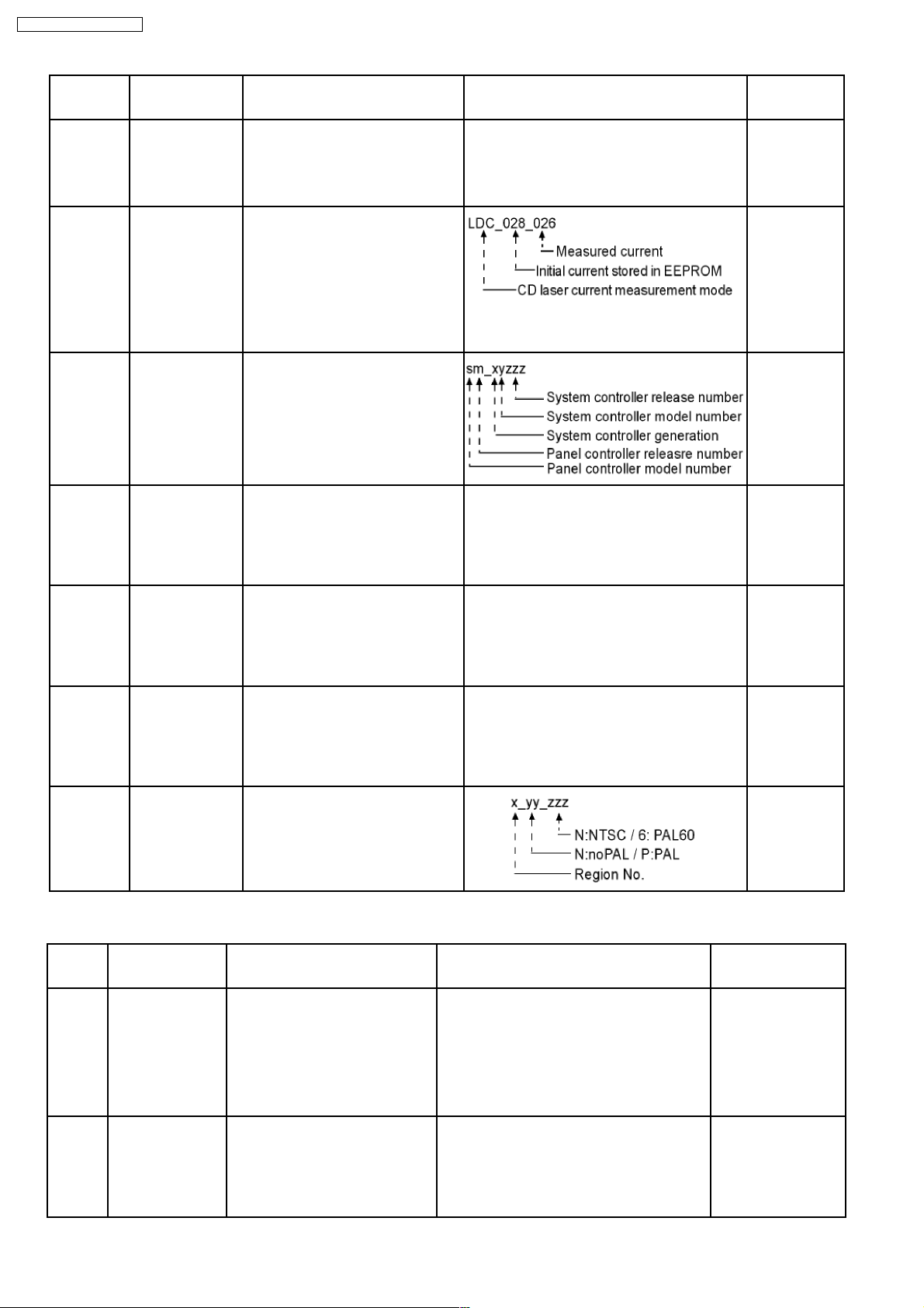
14.7. Service Mode Table 3
Item Player mode and
Timer 1
check
Timer 1
reset
button
combination
In STOP mode,
press PAUSE and
FWD-SKIP buttons
on the player, and
“5” button on the
remote control unit.
While displaying
Timer 1 data, press
STOP and FWDSKIP buttons on the
player, and “5”
button on the remote
control unit.
Timer 1 check.
Laser operation timer. Operation time
is measured separately for DVD laser
and CD laser.
Timer 1 reset.
Laser operation timer. Operation time
of both DVD laser and CD laser is
reset all at once.
Function Display Cancellation method
T1_1234_5678.
Shown to the left is DVD laser time, and to the
right is CD laser time.
Time is shown in 4 digits of decimal notation in a
unit of 10 hours.
“0000: will follow “9999”. (You may have to press
the “FL select” button on the remote control to
view the remaining text when the text is too long
to display on the FL at one time).
T1_0000_0000. (You may have to press the :FL
select” button on the remote control to view the
remaining text when the text is too long to display
on the FL at one time).
26
Cancelled
automatically 5
seconds later.
Cancelled
automatically 5
seconds later.
Page 27
DVD-F87GCS / DVD-F87GN
Item Player mode and
Timer 2
check
Timer 2
reset
button
combination
In STOP mode,
press PAUSE and
FWD-SKIP buttons
on the player, and
“6” button on the
remote control unit.
While displaying
Timer 2 data, press
STOP and FWDSKIP buttons on the
player and “6” button
on the remote
control unit.
Timer 2 check.
Spindle motor operation timer.
Timer 2 reset.
Spndle motor operation timer.
Function Display Cancellation method
T2_1234.
Time is shown in 4 digits of decimal notation in a
unit of 10 hours.
“0000” will follow “9999”.
T2_0000 Cancelled
Cancelled
automatically 5
seconds later.
automatically 5
seconds later.
14.8. Lock Function
This function prohibits removal of disc and some disc operations to prevent loss of disc at a shop during sales promotion or
equivalent occasions.
While this function is activated, the player displays “___LOCKED_” if any button is touched.
14.8.1. Setting
· Prohibiting removal of disc
1. Select the DVD/CD function.
2. Press and hold down the
seconds. (The message, “___LOCKED_” appears when the function is activated.)
Note:
OPEN/CLOSE
· Prohibiting operation of selector and disk
button are invalid and the player displays “___LOCKED_” while the lock function mode is entered.
1. Select the DVD/CD function.
2. Press and hold down the
seconds. (The message, “___LOCKED_” appears when the function is activated.)
Note:
The following buttons are invalid and the player displays “___LOCKED_” while the lock function mode is entered.
button on the player and the power button on the remote controller unit for at least three
button on the player and the power button on the remote controller unit for at least three
14.8.2. Exiting Lock Function
While the lock function is activated, press the buttons which are used to enter the mode. (“___LOCKED_” appears for one second,
and then “_UNLOCKED_” appears. (After this, the lock function is deactivated.)
14.9. Things to Do After Repair
Follow the procedure described below after repair.
1. While the power is on, press the
2. Press the power button to turn off the power.
3. Unplug the power cable.
Note:
It is prohibited to unplug the power cable while the tray is opened and to close the tray manually.
button to close the tray.
27
Page 28

DVD-F87GCS / DVD-F87GN
15 Service precautions
15.1. Recovery after the player is repaired
· When FLASH ROM or Module (2) P.C.B. is replaced, carry out the recovery processing to optimize the drive. Playback the
recovery disc to process the recovery automatically.
· Recovery disc (Product number=RFKZD03R005)
· Performing recovery
1. Load the recovery disc (Product number: RFKZD03R005) to the player and run it.
2. Recovery is performed automatically. When it is finished, a message appears on the screen.
3. Remove the recovery disc.
4. Turn off the power.
Note:
This unit requires no initialization process carried out after the traditional DVD players were repaired. When the recovery
measures are taken, the customer setting will return to the factory setting as same as the procedure described in item
“Initialization” in 13.6 is carried out. Write down the contents of the setting before recovery processing and reset the player.
15.2. DVD Player Firmware Version Upgrade Process
Firmware of DVD player may upgrade to conform to improvement of its performance and quality including operational range,
playability of non-standardized discs, etc. The version upgrade disc contains the recovery function, and the recovery disc is not
necessary.
Note:
Version upgrade process cannot be complete if the AC power is cut off due to power failure and other occasions during the
process. If this occurs, replace FLASH ROM and restart version upgrade. Version upgrade disc number is informed when
ordered.
15.3. Firmware Version Upgrade Process by Using Recovery Disc
· Recovery process
· Firmware version upgrade process
Both of the above procedures automatically start when the recovery disc is replayed.General CD-R disc allows version upgrade
process and recovery process, making version upgrade through disc simple.
Recovery process: Optimization process of player after replacement of FLASH ROM, EEPROM, or DVD Module Circuit board
Version upgrade process: Renewal of firmware for improvement of operational range and performance
15.3.1. Version Upgrade Process
1. Insert the recovery disc to the player to replay.
2. The version of player is automatically checked and prompts if necessary.
3. Select version upgrade process using the cursor keys on the remote controller unit. (Select YES or NO)
4. a. If YES is selected, the process starts.
b. If NO is selected, only the recovery process is applied.
28
Page 29

DVD-F87GCS / DVD-F87GN
5. a. When the version upgrade process is complete, a message of completion appears on the screen. Remove the disc.
b. Follow the instruction appearing on the screen, and remove the disc.
6. Turn off the power.
29
Page 30

DVD-F87GCS / DVD-F87GN
16 Disassembly and Main Compone nt Replacem ent
Procedures
16.1. Disassembly flow chart
The following chart is the procedure for disassembling the casing and inside parts for internal inspection when carrying out the
servicing.
To assemble the unit, reverse the steps shown in the chart as below.
30
Page 31

16.2. Printed Circuit Boards (P.C.B.) Position
DVD-F87GCS / DVD-F87GN
31
Page 32

DVD-F87GCS / DVD-F87GN
16.3. Disassembling of Top Cabinet
Step 1 Remove 4 screws.
Step 2 Remove 3 screws, and push the top cabinet backwards
to lift up.
16.4. Disassembling of DVD Lid
· Follow the (Step 1) - (Step 2) of Item 16.3.
Step 1 Keep the close lock gear pressed in clockwise, move
the tray assembly in the direction of the arrow.
16.5. Disassembling of Front Panel
· Follow the (Step 1) - (Step 2) of Item 16.3.
· Follow the (Step 1) - (Step 2) of Item 16.4.
Step 1 Release 2 claws on each side and 3 claws below the
unit.
Step 2 Disconnect FFC board connector (CN6004).
Step 2 Remove dvd lid.
Step 3 Release the close lock gear and slide the disc tray
backward as arrow shown.
Step 3 Draw the front panel unit forward.
Step 4 Remove 2 screws, draw the Panel P.C.B. forward.
Step 5 Remove 5 screws, Power P.C.B. and 10 Key P.C.B.
show.
32
Page 33

16.6. Disassembling of Rear Panel
· Follow the (Step 1) - (Step 2) of Item 16.3.
Step 1 Remove 5 screws.
16.7. Disassembling of Tray Assembly
· Follow the (Step 1) - (Step 2) of Item 16.3.
· Follow the (Step 1) - (Step 3) of Item 16.4.
Step 1 Keep the close lock gear pressed in clockwise, move
the tray assembly in the direction of the arrow.
DVD-F87GCS / DVD-F87GN
Step 2 Remove rear panel.
Step 2 Hold close lock gear, push and release the 4 claws in
the direction of arrow, and then remove the tray assembly.
Step 3 Detach FFC CN6002.
Step 4 Flip the tray, use extension cable to connect CN6002.
16.8. Disassembly of Main P.C.B.
· Follow the (Step 1) - (Step 2) of Item 16.3.
· Follow the (Step 1) - (Step 3) of Item 16.4.
· Follow the (Step 1) - (Step 5) of Item 16.5.
· Follow the (Step 1) - (Step 2) of Item 16.6.
Step 1 Remove 5 screws.
Step 2 Flip Main P.C.B.
33
Page 34

DVD-F87GCS / DVD-F87GN
16.9. Disassembly of Tray Base
Guide (L) and Tray Base Guide
(R)
· Follow the (Step 1) - (Step 2) of Item 16.8.
Step 1 Remove the 2 screws.
Step 2 Remove the tray base guide (L) and tray guide (R) in the
direction of arrow.
16.10. Disassembly of Tray Base
· Follow the (Step 1) - (Step 2) of Item 16.3.
· Follow the (Step 1) - (Step 3) of Item 16.4.
Step 1 Remove tray screw, tray spring and teflon washer.
Step 2 Remove rotary tray.
16.11. Disassembly of Open Lock
Gear
· Follow the (Step 1) - (Step 2) of Item 16.3.
· Follow the (Step 1) - (Step 3) of Item 16.4.
· Follow the (Step 1) - (Step 3) of Item 16.7.
34
Page 35

Step 1 Rotate open lock gear in the direction of arrow. (Anticlockwise)
DVD-F87GCS / DVD-F87GN
Step 2 Rotate close lock gear to direction of arrow, press claw
(b) and pull out close lock gear.
16.13. Disassembly of the Tray Motor
P.C.B. and Sensor P.C.B.
· Follow the (Step 1) - (Step 2) of Item 16.3.
· Follow the (Step 1) - (Step 3) of Item 16.4.
· Follow the (Step 1) - (Step 3) of Item 16.7.
Step 1 Remove 2 screws.
Step 2 Release claw of open lock gear, remove open lock gear
in the direction of arrow .
16.12. Disassembly of the Close
Lock Gear & Close Lock Gear
Spring
· Follow the (Step 1) - (Step 2) of Item 16.3.
· Follow the (Step 1) - (Step 3) of Item 16.4.
· Follow the (Step 1) - (Step 3) of Item 16.7.
· Follow the (Step 1) - (Step 2) of Item 16.10.
Step 2 Release 4 claws at Tray Motor P.C.B. and Sensor
P.C.B..
16.14. Disassembly of the CD
Traverse Unit
· Follow the (Step 1) - (Step 2) of Item 16.3.
· Follow the (Step 1) - (Step 3) of Item 16.4.
· Follow the (Step 1) - (Step 3) of Item 16.7.
Step 1 Remove 2 screws.
Step 2 Rotate cam gear anti-clockwise. (Align at position (B) as
marking on gear with arrow)
Step 1 Hold close lock spring to claw (a).
35
Page 36

DVD-F87GCS / DVD-F87GN
Step 3 Flip the base mech unit in vertical position.
Step 4 Press upward (a), push backward (b) and press to left
(c) to release CD traverse unit.
Step 5 DVD Module P.C.B. is show.
16.15. Disassembly of the Pulley
Gear
· Follow the (Step 1) - (Step 2) of Item 16.3.
· Follow the (Step 1) - (Step 3) of Item 16.4.
· Follow the (Step 1) - (Step 3) of Item 16.7.
Step 1 Remove of the Tray belt.
Step 3 Release the 2 claws in the direction of arrow (1), and
then push the pulley pin in the direction of arrow (2).
16.16. Disassembly of Loading Motor
P.C.B.
· Follow the (Step 1) - (Step 2) of Item 16.3.
· Follow the (Step 1) - (Step 3) of Item 16.4.
· Follow the (Step 1) - (Step 3) of Item 16.7.
Step 1 Remove 2 screws.
Step 2 Remove 2 screws.
Step 2 Flip the base mecha.
Step 3 Remove Loading Motor P.C.B.
16.17. Disassembly of Drive Gear (A)
& (B)
· Follow the (Step 1) - (Step 2) of Item 16.3.
· Follow the (Step 1) - (Step 3) of Item 16.4.
· Follow the (Step 1) - (Step 3) of Item 16.7.
36
Page 37

· Follow the (Step 1) - (Step 3) of Item 16.15.
Step 1 Release the claw in the direction of arrow (1), and then
push drive gear shaft up.
DVD-F87GCS / DVD-F87GN
16.19. Disassembly of Cam Gear &
Support Piece
· Follow the (Step 1) - (Step 2) of Item 16.3.
· Follow the (Step 1) - (Step 3) of Item 16.4.
· Follow the (Step 1) - (Step 3) of Item 16.7.
Step 1 Rotate (A) in cam gear anti-clockwise.
Step 2 Remove Drive Gear (A) and Drive Gear (B).
16.18. Disassembly of Magnet Holder
washer, Magnet and Clamper
· Follow the (Step 1) - (Step 2) of Item 16.3.
· Follow the (Step 1) - (Step 3) of Item 16.4.
· Follow the (Step 1) - (Step 3) of Item 16.7.
· Follow the (Step 1) - (Step 4) of Item 16.14.
Step 1 Release 3 claws in the direction of arrow.
Step 2 Remove 1 screw.
Step 3 Remove support piece.
16.20. Disassembly of Slide Plate (L)
& (R) and Change Lever
· Follow the (Step 1) - (Step 2) of Item 16.3.
· Follow the (Step 1) - (Step 3) of Item 16.4.
· Follow the (Step 1) - (Step 3) of Item 16.7.
· Follow the (Step 1) - (Step 5) of Item 16.19.
Step 1 Press the claw and push the Slide Plate (L) up.
37
Page 38

DVD-F87GCS / DVD-F87GN
Step 2 Remove slide plate (L) & (R) and change lever as arrow
shown.
Step 2 Make sure drive gear (A) at vertical position.
Step 3 Push tray base to the direction of arrow shown.
16.21. Assembly of Tray Base
Step 1 Rotate cam gear anti-clockwise. Align at position (C) as
marking on gear with arrow.
38
Page 39

DVD-F87GCS / DVD-F87GN
17 Service Position
17.1. Checking Procedure
Note:
For the disassembling procedure, see Section 16.
17.2. Checking the Main P.C.B. , Panel P.C.B, Selection Panel P.C.B. and
Display Panel P.C.B.
1. Disassembly of Top Cabinet.
2. Disassembly of DVD Lid.
3. Disassembly of Panel, 10 Key & Sensor P.C.B..
4. Disassembly of Rear Panel.
5. Disassembly of tray assembly.
6. Disassembly of Main P.C.B.
39
Page 40

DVD-F87GCS / DVD-F87GN
18 Adjustment Procedure s
18.1. Service Tools and Equipment
18.1.1. Usage Equipment
Application Name Number
Tilt adjustment DVD test disc DVDT-S15 or DVDT-S01
TORX screw driver (T6) Available on sales route. (T6) or
Others Hanari VFK1784
Grease RFKXPG641
Drysurf RFKXGUD24
Confirmation CD test disc PVCD-K06 and any other
Recovery disc RFKZD03R005
18.1.2. Important points in adjustment
18.1.2.1. Important points in Optical Adjustment
· Before starting optical system adjustment, be sure to take anti-static measures.
· Optical adjustment (optical pickup tilt adjustment) is required after following parts are replaced:
1. Optical pickup unit.
2. Spindle motor assembly unit.
3. Optical pickup peripherals (such as a rail)
Note:
Optical adjustment is not necessary after replacement of other parts inside the traverse unit. However, may require when picture
deterioration is detected. Optical adjustments cannot be applied to the inside of optical pickup. When a traverse unit is replaced,
the adjustment is not necessary.
RFKZ0185
commercially available disc
18.1.3. Storing and Handling Test Discs
Surface precision is vital for DVD test discs. Be sure to store and handle them carefully.
· Do not place discs directly onto the workbench, etc, after use.
· Handle the discs carefully in order to maintain their flatness. Place them into their case after use and store them vertically. Store
discs in a cool place where they are not exposed to direct sunlight or air from air conditioned.
· Accurate adjustment will not be possible if the disc is warped when placed on a surface made of glass, etc. If this happens, use
a new test disc to make optical adjustments.
· If adjustment is done using a warped disc, the adjustment will be incorrect and some discs will not be playable.
40
Page 41

18.1.4. Optical Adjustment (Optical Pickup Tilt Adjustment)
Measurement point Adjustment point Mode Disc
Tangential adjustment screw
Tilt adjustment screw
Measuring equipment Adjustment value
None (LCD display of the player is used.) Adjust that jitter value becomes minimum.
T1 (inner track) replay
T43 (outer track) replay
DVD-F87GCS / DVD-F87GN
DVDT-S15 or DVDT-S01
18.1.4.1. Adjustment Procedure
1. While the player is stopped and no disc is inserted, select
the DVD function. Press and hold down the
the player and the number button, “5” on the remote
controller unit.
2. Check that “J_xxx_yyy_zz” is appearing on the display.
For your information:
The values, “yyy” and “zz” are not associated to jitter
value.
“yyy” indicates the frequency of error occurrence.
“zz” indicates the focus drive value.
Note:
Jitter value appears on the display.
3. Play test disc T30 (central periphery).
4. Adjust tangential adjustment screw so that the jitter value is
minimized.
5. Play test disc T30 (central periphery).
6. Adjust tilt adjustment screw 1 so that the jitter value is
minimized.
7. Play test disc T30 (central periphery).
8. Adjust tilt adjustment screw 2 so that the jitter value is
minimized.
9. Repeat adjusting tilt adjustment screws 1 and 2 alternately
until the jitter value is minimized.
10. Finally please reproduce T01 (inner periphery) and T43
(outer periphery) and check the jitter value. (Please
readjust, when the jitter value is extremely different.)
button on
adjustment.
2. Repeat adjusting two or three times to find the optimum
point.
3. Finish the procedure with tilt adjustment.
18.1.4.3. Check After Adjustment
Play test disc or any other disc to make sure there is no picture
degradation in the inner, middle and outer peripheries, and no
audio skipping. After adjustment is finished, lock each
adjustment screw in position using screw lock.
18.1.4.4. Procedure for Screw Lock
1. After adjustment, remove top cover, tray, clamper base and
traverse unit in this sequence.
2. Lay the traverse unit upside down, and fix adjustment screw
with screw lock.
3. After fixing, reassemble traverse unit, clamper base, tray
and top cover.
Fig. 18-1
18.1.4.2. Tips
1. Make tangential adjustment first, and then make tilt
Fig. 18-2
41
Page 42

DVD-F87GCS / DVD-F87GN
19 Illustration of IC’s, Transistor s and Diodes
C9ZB00000431 (34p)
C3ABPG000068 (54p)
1
C0DBZHG00017 (5P)
1
5
2SB14170JA
B
C
E
2SC3311ASA
B
C
E
XN0431100L
4
5
3
2
1
1
1
6
C0GBG0000033
C0GBF0000004
C0GBG000044
28
22
21
7
8
14
C0EBE0000106
3
1
2SC22950XL
2
C0EBE0000384
2SB1219AHL
1
2
B3ABA0000397
C0ABBB000118
5
8
15
4
1
B3RAD0000035
2
3
2
1
B1BCCD000013
3
C0EBA0000031
C0GAG0000007
C0CBCBD00018
C3EBGC000055
B1DDCC000009
1
2
3
XN0150100L
6
C0DAEMZ00001
1
3
1
2
B0HAGM000006
A
Anode
5
4
5
4
3
B3AAA0000534
Ca
Cathode
Anode
Cathode
A
C0FBBK000036 (48P)
MN101C28DHA (80P)
MN101C07AHB (64P)
MN2DS0003APH
C3FBMD000134
5
4
3
2
Ca
B0EDKT000002
4
2
2SD132800L
2SD0601AHL
2SD1819A0L
UNR221300L
UNR221200L
UNR221100L
UNR511F00L
UNR521100L
MA2J11100L
C0DACZH00006 (5P)
C0DACZH00007 (5P)
C0JBCA000066 (5P)
B3NAB 0000027
B3NAA0000068
B3PBA0000104
1
2SB09700RL
UNR511V00L
1
2
MAZ41800MF
A
Anode
Ca
Cathode
3
MAZ42000LF
MAZ41000HF
MAZ41000mF
MAZ41600LF
A
Anode
Ca
Cathode
MA2J72800L
MA2C16500E
B0JAME000037
MA2S11100L
B0HADV000001
42
Page 43

20 Block Diagram
OPTICAL PICKUP
DVD-F87GCS / DVD-F87GN
B
QR8571
CONTROL
HFM
VCC
HFN
SUPPLY
SWITCH
Q8552
Q8551
OUT
LDDVD
SWITCH
SWITCH
Q8562
Q8561
LDCD
SWITCH
SWITCH
LDU
17
LD(DVD)
16
LD(CD)
15
SW
8
SUBSEL
1M
PIN(CD)
PIN(DVD)
VREF
SUB2
SUB1
13
11
14
SUB1
SUB2
VREF1
RF
9
RF
VREF2 (RF-)
FE2
FE1
7
6
FE1(DVD/CD)
FE2(DVD/CD)
TC
4
TC(DVD)
TD
5
TD(DVD)
TB
2
TB(DVD)
3
TA(DVD)
TA
TRACKING COIL
T-
T+
14
13
V01-
VIN3
23
FOCUS COIL
F-
F+
11
12
V02-
V01+
V02+
IC8251
C0GBG0000044
MOTOR DRIVE
VIN1
MUTE3
MUTE12
27
9
2
FEED-
FEED+
17
18
V03+
OPIN+
BIAS2
VIN2
IDCNT
3
28
V03-
BIAS
LDIN
TRIN
1
4
24
21
25
26
SPINDLE MOTOR UNIT
HU-
HU+
COIL_U
COIL_V
COIL_W
9
10
4
7
2
A1
A2
A3
ECR
IC8271
C0GBF0000004
MOTOR DRIVE
EC
22
H1-
H1+
23
H-
HV-
HV+
HW+
12
13
11
H2-
H2+
PS
24
SW
HW-
15
14
VH
H3-
H3+
FG
R
146
147
PWM1
VCOF/AD4
139
148
140
128
PWM0
VHALF
AD1
P9
59
6
IC8611
C3EBGC000055
EEPROM
(NOT SUPPLIED)
AD2
79
76
DRV1
DRV4
P8
60
5
81
72
FG
DRV6
LSI
83
75
DRV0
DRV8
111
RFINN
132
RFINP
131
VIN7
136
VIN8
VIN3
135
115
VIN3RF
137
114
116
VIN2
VIN4
VIN4RF
MN2DS0003APH
138
VIN2RF
117
VIN1
IC8001
VIN1RF
LPC01
126
143
AD0
LPC02
78
124
DRV3
130
123
82
125
LPC1
LPC2
DRV7
127
129
VIN5
133
OSCO
X8621
VIN10
110
VIN6
VREFH
OSCI
165
134
VIN9
166
43
Page 44

DVD-F87GCS / DVD-F87GN
Q8560
D8550
Q8550
SWITCH
SWITCH
B
IC8601
C0EBE0000384
VOLTAGE
DETECTOR
DQ0
2,4,5,7,8,10,11,
13,42,44,45,47,
48,50,51,53
1,2,4,5,7,8,10,
11,13-15,17,18,
252,254,256
MDQ0
DQ15
MDQ15
A0
22-26,
29-35
217,220,221,223,
224,226-228,230,
233,237,238
MA0
IC8051
C3ABPG000068
64MB SDRAM
A11
20
234
MA11
IC8651
GCS: RFKFCF81J160
GN: RFKFCF81H160
FLASH ROM
BA0
232
BA0
19
39
15
21
240
243
251
249
BA1
DQM1
DQM0
NCSM
/CS
UDQM
BA1
LDQM
/RAS
/CAS
CLK
38
241
MCK
MCKI
/WE
17
18
16
244
245
248
NWE
NCAS
NRAS
A16
9,10,16,17,48
21,30,31,43,45
EXADR16
MN2DS0003APH
A20
EXADR20
A0
1-8,18-25
23-25,27,32,
33,36,37,39-42,
46,47,50,51
EXADT0
IC8001
A15
192-195,197-200,
203,204,206-208,
EXADT15
LSI
DQ0
29-36,
38-45
210-212
MDQ16
DQ15
MDQ31
XWE
11
22
NEXWE
26
38
XRESET
XCE
28
52
NEXCE
XOE
NEXOE
12
Q8606
SWITCH
Q8605
SWITCH
IC8605
C0EBA0000031
RESET IC
73
NRST
R
44
Page 45

DVD-F87GCS / DVD-F87GN
MIXL(R)
FL(R)
SL(R)
CNT
Y
PR/CR/R
C
CMD
IECOUT
STATUS
SW
PY/Y/G
ZFLAG&AMUTE
PB/CB/B
DSPCLK
A
TO MAIN
BLOCK
B
12(11)
14(13)
16(20)
VOUT7(8)
VOUT1(2)
IC8451
DIN3
LRCIN
41
31
C0FBBK000036
AUDIO DAC
BCKIN
DATA4
40
37
RSTB
DIN1
45-47
38
10
VOUT3(4)
SCLKI
33
MDO
VOUT5
34
9
MDI
VOUT6
35
ZFLGA
ML
MC
36
QR8420
48
MUTING
SWITCH
4
IC8695
C0JBCA000066
AND GATE
LOGIC IC
1
2
1
IC8111
C0CBCBD00018
POWER
SUPPLY
5
8
5
5
4
IC8691
C0JBCA000066
AND GATE
LOGIC IC
1
2
174-176
ADOUT0
169
ADOUT2
171
LRCK
170
ADOUT3
163
SRCK
58
DACCK
53
57
P11
P10
55
56
P12
P13
P15
149
DAC1OUT
MN2DS0003APH
151
152
DAC2OUT
IC8001
156
DAC3OUT
DAC4OUT
LSI
158
70
DAC5OUT
177
P1
IECOUT
69
P2
68
P3
45
Page 46

DVD-F87GCS / DVD-F87GN
TO CD DRIVE
BLOCK
A
C
Y
PY/Y/G
PB/CB/B
PR/CR/R
MIXL(R)
FL(R)
SL(R)
IC4301
C0ABBB000118
OP-AMP (WITH
TONE CONTROL)
2(6)
3(5)
IC4302
C0ABBB000118
OP-AMP (WITH
TONE CONTROL)
2(6)
3(5)
IC4303
C0ABBB000118
OP-AMP (WITH
TONE CONTROL)
2(6)
3(5)
JK4501
14(13)
11(10)
SVIDEO
24
C
25
Y
20
Y
19
VOUT
17
PB
16
PR
MIX_L(R)
FL(R)
8(7)
SL(R)
33
COUT
28
YOUT
CYOUT
CYSAG
CBOUT
CBSAG
CROUT
CRSAG
Q4419
(Q4410)
Q4413
(Q4414)
YSAG
VOUT
VSAG
MUTING
SWITCH
(AUDIO)
MUTING
SWITCH
(AUDIO)
27
25
24
31
30
22
21
19
18
2
CIN
6
YIN
IC3501
12
CYIN
C9ZB00000431
VIDEO
14
CBIN
SELECTOR
16
CRIN
1(7)
1(7)
1(7)
CNT
SW
IECOUT
ZFLAG&AMUTE
CMD
STATUS
DSPCLK
IC4304
C0ABBB000118
OP-AMP (WITH
TONE CONTROL)
6
5
2
3
B
Q4415
(Q4416)
MUTING
SWITCH
(AUDIO)
7
1
Q4417
MUTING
SWITCH
(AUDIO)
18
19
20
SYS-CMD
SYS-STAT
SYS-DSPCLK
Q4418
MUTING
SWITCH
(AUDIO)
QR4302
MUTING
CONTROL
Q4302
MUTING
SWITCH
53
MN101C28DHA
B
POWER-MUTE
IC6001
5
CNT
4
SW
JK4502
DIGITAL
Q4511
SWITCH
AUDIO OUT
COAXIAL
8 BIT 1-CHIP MICROCONTROLLER
B
QR3541
SWITCH
54
WIDE-1
46
Page 47

M
M9001
LOADING MOTOR
Q9103
PHOTO
COUPLER
Q9102
PHOTO
COUPLER
DVD-F87GCS / DVD-F87GN
1
33-41
XRST
9G
DGT15
P66/DGT16
DISC1-5,
CDMODE
F-
F+
45
32
26-28,
58-60
Q6571
SWITCH
QR6591QR6597
LED
DRIVER
FROM POWER
TRANSFORMER
D6641D6647
B
IC6062
4
C0GAG0000007
CHANGER
2
M
M9101
TRAY MOTOR
IC6061
4
C0GAG0000007
CHANGER
2
MOTOR
DRIVER
7
9
QR6061
SWITCH
B
MOTOR
DRIVER
7
1
QR6062
1
SWITCH
9
S6531-S6533,
S6731-S6736
S6521-S6524,
S6721-S6726
S6511,
S6611-S6618
6
5
4
AN5
AN4
AN3
P1
13,14,16,18,20,
23,25,27,30,32
47-56
SEG6
DP6501
FL DISPLAY
P10
SEG15
IC6501
MN101C07AHB
MICROCONTROLLER
P11
34,36,39-41
42-46
DGT2
P15
10,15,19,22,26,
DGT6
1G
29,33,37,42
DGT7
B
Q9001
PHOTO COUPLER
IC6551
B3RAD0000035
INFRARED
IC
21
IHQ0/P20
OSC1
OSC2
10
9
X6501
SBI1
SBO1
SBT1
62
15
61
63
Q9101
PHOTO
COUPLER
33
34
POSITION
45
44
5
AN3
LONG-F
LONG-R
PULSE-SENSOR
S9001
LOADING
32
31
OPEN-SW
CAM-SENSOR
MN101C28DHA
RST
25
IC6011
C0EBE0000106
RESET IC
28
IC6001
46
47
PWM
TRAY-F
TRAY-R
8 BIT 1-CHIP MICROCONTROLLER
OSC1
OSC2
13
12
X6001
21
22
FL-CMD
FL-STAT
23
FL-DSPCLK
56
FL_RESET_L
47
Page 48

DVD-F87GCS / DVD-F87GN
TO
FL DISPLAY
T1021
Q4901
SWITCH
B
Q4911
SWITCH
B
QR4902
QR4901
SWITCH
SWITCH
B
B
B
B
IC1155
C0DBZHG00017
POWER
SUPPLY
2
IC1151
C0DBZHG00017
POWER
SUPPLY
2
Q1125,Q1126
SWITCH/
REGULATOR
Q1115
SWITCH
(POWER
ON/OFF)
QR1115
SWITCH
1
P1001
AC
D1151,
1
D1152
D1011
L1001
D1002
INLET
F1001
B
D1121
POWER TRANSFORMER
Q1082
REGULATOR
D1111
D1082
D1083
D1041
Q1081
REGULATOR
D1084
MN101C28DHA
52
NPOFF_L
IC6001
8 BIT 1-CHIP MICROCONTROLLER
SIGNAL LINES
B
B
: MAIN SIGNAL LINE
: CD-DA (AUDIO /VIDEO) SIGNAL LINE
( ) Indicates the Pin No. of Right Channel.
D1141
D1071
D1072
Q1051
PHOTO COUPLER
1
IC1101
3
C0DAEMZ00001
VOLTAGE
REGULATOR
: DVD AUDIO SIGNAL LINE
: DVD VIDEO SIGNAL LINE
NOTE : Signal Lines are applicable to the Left Channel only.
1
5
IC1021
C0DACZH00007
POWER
SUPPLY
2
Q1045
4
REGULATOR
ZA1111
48
Page 49

21 Schematic Diagram
(All schematic diagrams may be modified at any time with the
development of the new technology)
Note:
S6511 : O/C switch
S6521 : Disc - EXC switch
S6522 : Disc Skip switch
S6523 : F- skip switch
S6524 : R- skip switch
S6531 : Stop switch
S6532 : Pause switch
S6533 : Play switch
S6611 : Power switch
S6612 ~ S6616 : Disc 1 - 5 switch
S6617 : CD Mode switch
S6618 : DPL II switch
S6721 : [10] switch
S6722 : [5] switch
S6723 : [4] switch
S6724 : [3] switch
S6725 : [2] switch
S6726 : [1] switch
S6731 : [CANCEL] switch
S6732 : [0] switch
S6733 : [9] switch
S6734 : [8] switch
S6735 : [7] switch
S6736 : [6] switch
S9001 : Loading switch
· The voltage value and waveforms are the reference voltage
of this unit measured by DC electronic voltmeter (high
impedance) and oscilloscope on the basis of chassis.
Accordingly, there may arise some error in voltage values
and waveforms depending upon the internal impedance of
the tester or the measuring unit.
No mark : Playback << >> Rec <> :FM
(( )) :CD () :AM [] : AUX
DVD-F87GCS / DVD-F87GN
· Importance safety notice :
Components identified by
characteristics important for safety. Furthermore, special
parts which have purposes of fire-retardant (resistors), highquality sound (capacitors), low-noise (resistors), etc. are
used. When replacing any of components, be sure to use
only manufacturer´s specified parts shown in the parts list.
Caution !
IC, LSI and VLSI are sensitive to static electricity.
Secondary trouble can be prevented by taking care during
repair.
· Cover the parts boxes made of plastics with aluminium foil.
· Put a conductive mat on the work table.
· Ground the soldering iron.
· Do not touch the pins of IC, LSI or VLSI with fingers directly.
mark have special
49
Page 50

DVD-F87GCS / DVD-F87GN
21.1. (A) Optical Pickup Unit Circuit
SCHEMATIC DIAGRAM - 1
HFM
PCB
LDU
PCB
TO
TO
OPTICAL PICKUP UNIT CIRCUIT
1
2
3
4
5
6
1
2
3
4
5
6
7
8
9
10
11
12
13
14
15
16
17
18
GND
VCC
GND
GND
OUT
GND
GND
TB
TA
TC
TD
FE1
FE2
IM
RF
GND
VREF
VCC
SUB2
SUB1
SW
LD (CD)
LD (DVD)
LDGND
L4
J0JBC0000105
L3
J0JBC0000105
C8
0.1
: +B SIGNAL LINE : CD-DA SIGNAL LINE
T+
26
F+
25
HFM
FE2
FE1
GND (IM)
VREF2(RF-)
PIN (DVD)
LD (CD)
LD GND
LD (DVD)
GND (OEIC)
VREF1
VCC
SUB2
SUB1
PIN(CD)
GND (IM)
F-
24
T-
23
22
TA
21
TB
20
TD
19
TC
18
17
16
TO
15
DVD
RF
14
MODULE
13
(IN/OUT)
12
CIRCUIT
11
(FP8501) ON
10
SCHEMATIC
9
DIAGRAM-2
8
7
6
5
4
3
SW
2
1
TO ACT
R2
0
R4
C2
0
0.1
C1
0.1
C3
0.1
R1
0
R3
0
R5
0
R6
0
VR1
6.8K
C5
22PC622P
6.8K
L2
J0JCC0000307
L1
J0JBC0000105
R7
VR2
6.8K
C7
0.1
C4
0.22
50
Page 51

21.2. (A) DVD Module (In/Out) Circuit
SCHEMATIC DIAGRAM - 2
DVD-F87GCS / DVD-F87GN
SPINDLE
PCB
TO
FP8271
1
2
3
4
5
6
7
8
9
10
11
12
13
14
15
DVD MODULE (IN/OUT) CIRCUIT
COIL_W
COIL_V
COIL_U
H+
HU+
HUHV+
HVHW+
HWHSW(GND)
SW
FEEDFEED+
TC8271
TC8272
TC8273
TC8274
TC8275
TC8276
TC8277
TC8278
TC8279
TC8280
TC8281
TC8282
TC8283
TC8284
TC8285
R8281 100
R8282 100
TRV-INNER-SW DV2
LB8271
ERJ3GEY0R00V
LB8272
ERJ3GEY0R00V
LB8273
ERJ3GEY0R00V
: +B SIGNAL LINE : CD-DA SIGNAL LINE
NC
1
A3
2
NC
3
4
A2
IC8271
C0GBF0000004
MOTOR DRIVE IC
C8275
0.1
C8284
0.01
C8285
0.01
C8286
0.01
NC
5
6
NC
A1
7
FIN
IC8271
GND
8
H1+
9
H1-
10
11
H2+
H2-
12
H3+
13
14
H3-
RNF
GSW
VCC
ECR
FG2
CNF
28
Vm
27
26
25
FG
24
23
PS
EC
22
FIN
3029
21
FR
CP8273
20
19
CP8272
18
SB
17
C8287
0.1
BR
16
15
VH
TO
OPTICAL
PICKUP
UNIT
CIRCUIT
ON
SCHEMATIC
DIAGRAM-1
FP8501
T+
26
F+
25
F-
24
T-
23
HFN
22
TA(DVD)
21
TB(DVD)
20
TD(DVD)
19
TC(DVD)
18
FE2(DVD/CD)
17
FE1(DVD/CD)
16
GND
15
RF
14
VREF2(RF-)
13
PIN(DVD)
12
LDCD
11
LDGND
10
LDDVD
9
GND(OEIC)
8
VREF1
7
VCC
6
SUB2
5
SUB1
4
PIN(CD)
3
SUBSEL
2
GND(VRCD)
1
TP8251
TP8253
TP8254
TP8252
TP8502
TP8514
TP8515
TP8517
TP8516
TC8504
TC8503
TP8519
TP8518
TP8511
TP8520
TP8510
TP8501
TC8501
TP8525
TP8524
TP8521
TC8502
TP8500
C8504 0.1
TRDRVDV2
FODRVDV2
MUTE12 DV2
IC8251
C0GBG0000044
MOTOR DRIVE IC
LB8512 ERJ3GEY0R00V
LB8513 ERJ3GEY0R00V
LB8511 ERJ3GEY0R00V
LB8514 ERJ3GEY0R00V
LB8506 D0GB152JA002
LB8505 J0JCC0000091
LB8504 J0JCC0000091
LB8503 ERJ3GEY0R00V
LB8501 ERJ3GEYJ222V
R8501 0
BIAS1
1
VIN1
2
VIN2
3
4
OPIN+
OPIN-
5
OPOUT
6
GND(PRE)
7
FIN
VCC(CH1.2)
8
MUTE12
9
GND(CH1.2)
10
VO2-
11
VO2+
12
VO1-
13
14
VO1+
IC8251
VCC(CH3.4)
GND(CH3.4)
LDCNT
MUTE3
TRIN
BIAS2
LDIN
VIN3
PREVCC
FIN
MUTE4
VO3-
VO3+
VO4-
VO4+
28
27
26
25
24
23
22
3029
21
20
19
18
17
16
CP8252
15
CP8251
51
Page 52

DVD-F87GCS / DVD-F87GN
SCHEMATIC DIAGRAM - 3
DVD MODULE (IN/OUT) CIRCUIT
: +B SIGNAL LINE
: DVD AUDIO SIGNAL LINE
: CD-DA SIGNAL LINE
C8255
0.1
C8261
C8252
16V22
0.1
R8271 0.39
RA8271
(10K x 2)
C8288
0.1
C8274
TRSDRV DV2
R8251 6.8
C8272
0.1
6.3V33
FG DV2
MUTE3 DV2
SPDRV DV2
VHALF DV2
C8253
C8251
6.3V220
C8112
CP8423
R8451
CP8421
CP8422
1
C8113
470P
0
ADOUT0DV2
ADOUT1DV2
ADOUT2DV2
C8453
C8455
10V10
C0CBCBD00018
POWER SUPPLY IC
1
VO
2
NC
IC8111
3
GND
4
CN
2SB1219AHL
0.1
IC8111
Q8550
SWITCH
Cont
CP8424
CP8425
CP8426
C8456
0.1
8
VIN
7
NC
6
NC
5
C8111
0.1
L8550
G1C100KA0055
DMIXOUTDV2
SBI3DV2
SBO3DV2
SBT3DV2
STBDACDV2
PNRSTDV2
ADAC-CLKDV2
SRCKDV2
LRCKDV2
0.1
LB8420
J0JCC0000091
C8271
16V47
C8273
0.1
QR8571
UNR511V00L
SWTCH
(SUPPLY CONTROL)
CP8571
D+3.3VDV2
L8420
G1C220KA0055
TP8111
HFMON DV2
QR8571
C8254
0.1
RA8503
(56 x 2)
RA8501
(56 x 2)
RA8502
(56 x 4)
RA8504
(56 x 2)
C8506
100P
CP8502
CP8501
C8505
220P
VIN1 DV2
VIN2 DV2
VIN4 DV2
VIN3 DV2
VIN8 DV2
VIN7 DV2
RFINP DV2
RFINN DV2
LPC1 DV2
VREFH DV2
VIN6 DV2
VIN5 DV2
LPC2 DV2
RAM_CD DV2
D8571
MA2J72800L
LB8507
J0JCC0000091
C8502
0.1
LB8502
J0JHC0000045
C8501
10V10
C8503
TP8523
C8561
0.1
R8567
51
R8568
47K
C8551
0.1
R8559
15K
0.1
C8563
6.3V47
R8566
56
TP8522
R8565
2SB09700RL
2SD1819A0L
AD0 DV2
R8557
51
R8558
47K
Q8552
2SB09700RL
SWITCH
2.2
Q8562
SWITCH
Q8560
SWITCH
R8556
56
R8563
1K
TP8512
R8564
10
TP8513
C8553
6.3V47
R8555
C8564 1
2.2
16V10
C8562
R8562
2SD1819A0L
330
R8553
1K
R8554
Q8551
2SD1819A0L
SWITCH
22
R8550
7.5K
R8560
1K
R8570
100K
R8561
Q8561
SWITCH
C8554 1
R8552
330
0
C8550
6.3V33
R8569
12K
Q8560
C8552
16V10
R8551
0
Q8550
52
Page 53

SCHEMATIC DIAGRAM - 4
DVD MODULE (IN/OUT) CIRCUIT
C8423
0.1
C8424
0.1
: MAIN SIGNAL LINE
: +B SIGNAL LINE
DVD-F87GCS / DVD-F87GN
: DVD AUDIO SIGNAL LINE
: DVD VIDEO SIGNAL LINE
CP8561
D8550
MA2S11100L
37
RSTB
38
SCLKI
39
SCLKO
40
BCKIN
41
LRCIN
TEST
42
43
VDD
44
DGND
45
DIN1
46
DIN2
DIN3
47
48
ZFLGA
C8462
0.1
OP_CPU-CLKDV2
LPCO2 DV2
33
3536
32
34
ML
MC
MDI
MDO
C0FBBK000036
AUDIO DAC
ZFLG1
ZFLG2
ZFLG3
ZFLG4
1
4
3
2
R8420
2.2K
J0JCC0000091
28
293031
NC
DATA4
ZERO8
ZERO7
IC8451
ZFLG5
ZFLG6NCNC
8
67
5
QR8420
UNR521100L
AUDIO MUTING
SWITCH
LB8690
VCC
VOUT6
9
27
10
26
AGND
VOUT5
11
25
VCC
VOUT4
12
C8451
10V10
AGND
24
VCC
23
AGND
22
VCC
AGND
21
20
VOUT8(NC)
19
AGND
VCC
18
17
AGND
16
VOUT7(NC)
VOUT1
VOUT2
VOUT3
C0JBCA000066
AND GATE LOGIC IC
2
3
GND
VCOM
IC8691
C8461
15
14
13
VCC
C8452
C8420
10V10
6.3V330
FP8101
VGND
1
Y/PY/GDV2
CB/PB/BDV2
CR/PR/RDV2
YDV2
CDV2
6.3V100
QR8420
AMUTDV2
AUDIODIGITALDV2
A+5VDV2
D+1.2VDV2
51
4
C8691
0.1
LB8303 TC8303J0JCC0000119
LB8304 TC8304J0JCC0000119
LB8305 TC8305J0JCC0000119
LB8301 TC8301J0JCC0000119
LB8302
K8421
LB8421 TC8423
LB8422 TC8424
LB8451 TC8425J0JCC0000119
LB8452 TC8426J0JCC0000119
LB8453 TC8427J0JCC0000119
LB8454 TC8428J0JCC0000119
LB8455 TC8429J0JCC0000119
LB8456 J0JCC0000119
TC8430
LB8423 TC8431ERJ3GEY0R00V
LB8424 TC8432
TC8491 J0JCC0000119
LB8491
LB8691 TC8691D0GB101JA002
LB8692 TC8692
LB8693 TC8693
J0JCC0000119
J0JCC0000119
J0JCC0000091
FL8103
F1H0J1050022
FL8102
F1H0J1050022
FL8101
F1H0J1050022
FL8104
F1J1E1040022
D0GB101JA002
D0GB101JA002
TC8000
TC8006
TC8302J0JCC0000119
TC8421
TC8422
TC8105
TC8104
TC8103
TC8102
TC8101
K8100
TC8108
TC8107
K8002
K8007
FOR F87GCS ONLY
Y/PY/G
VGND
CB/PB/B
VGND
CR/PR/R
VGND
VGND
ADAC5V
MIX-L
ADAC5V
MIX-R
ADACGND
ADACGND
ADACGND
ADACGND
ADACGND
CNT
ADACGND
A-REF
ZFLAG&AMUTE
DGND
AUDIODIGITAL
DGND
D+5V
DGND
D+5V
DGND
A+5V
AGND
A+5V
AGND
D+1.2V
DGND
D+1.2V
DGND
M+9V
MGND
M+9V
MGND
OP_CPU-CLK
OP_CPU-CMD
OP_CPU-STAT
TC8002
TC8008
Y
C
FL
FR
SL
SR
SW
2
3
4
5
6
7
8
9
10
11
12
13
14
15
16
17
18
19
20
21
22
23
24
25
26
27
28
29
30
31
32
33
34
35
36
37
38
39
40
41
42
43
44
45
46
47
48
49
50
TO
MAIN
(AUDIO-OUT1)
CIRCUIT
(PS4001) ON
SCHEMATIC
DIAGRAM-11
CP8551
OP_CPU-CMDDV2
OP_CPU-STATDV2
LPCO1 DV2
IC8695
C0JBCA000066
AND GATE LOGIC IC
VCC
2
3
GND
TC8000
TC8000
TC8006
51
C8695
0.1
4
TC8006
K8003
K8005
K8008
K8010
FOR F87GN ONLY
TC8003
TC8005
TC8009
TC8011
53
Page 54

DVD-F87GCS / DVD-F87GN
21.3. (A) DVD Module (DV2) Circuit
SCHEMATIC DIAGRAM - 5
DVD MODULE (DV2) CIRCUIT
IC8611
C3EBGC000055
EEPROM IC
(NOT SUPPLIED)
1
A0
2
A1
IC8611
3
A2
4
GND
8
VCC
RA8611
(4.7K x 2)
7
WP
6
SCL
5
SDA
STBDACI/O
AMUTI/O
SBT3I/O
SBO3I/O
SBI3I/O
CP8021
CP8022
CP8023
CP8024
CP8025
CP8026
CP8027
CP8028
CP8029
CP8030
R8021 10K
RA8021
(10K x 2)
R8611
100
C8611
0.1
CP8612
CP8611
: +B SIGNAL LINE
PNRST
SCL
SDA
STBDAC
RSTCNT
AMUT
SBT3
SBO3
SBI3
WIDE_L
RGBH
CLKSEL
YC_H
EXADT15
EXADT14
EXADT13
EXADT12
EXADT11
EXADT10
EXADT9
EXADT8
EXADR19
EXADR20
NEXWE
EXADR18
EXADR17
EXADT7
EXADT6
EXADT5
EXADT4
EXADT3
EXADT2
EXADT1
GCS: RFKFCF81J160
GN: RFKFCF81H160
A15
1
A14
2
A13
3
A12
4
A11
5
6
A10
7
A9
8
A8
9
A19
10
A20
XWE
11
12
XRESET
NC
13
K8651
WP/ACC
14
RDY/XBSY
15
A18
16
A17
17
A7
18
19
A6
20
A5
A4
21
A3
22
A2
23
24
A1
IC8651
FLASH ROM IC
DQ15/A-1
XBYTE
VSS
DQ7
DQ14
DQ6
DQ13
DQ5
DQ12
DQ4
VDD
DQ11
DQ3
DQ10
DQ2
DQ9
DQ1
DQ8
DQ0
XOE
VSS
XCE
A16
EXADR16
48
47
46
FDT15
45
FDT7
44
FDT14
43
FDT6
42
FDT13
41
FDT5
40
FDT12
39
FDT4
38
37
FDT11
C8651
36
FDT3
35
FDT10
34
FDT2
33
FDT9
32
FDT1
31
FDT8
30
FDT0
29
28
27
26
EXADT0
25
A0
C8652
0.1
0.1
OP_CPU-CLKI/O
OP_CPU-STATI/O
OP_CPU-CMDI/O
TRSDRVI/O
SPDRVI/O
HFMONI/O
TRV-INNER-SWI/O
MUTE3I/O
RAM_CDI/O
MUTE12I/O
FGI/O
PNRSTI/O
CP8031
CP8032
CP8033
CP8242 CP8241
C8241
0.1
CP8244 CP8243
C8242
0.1
R8022 10K
R8241
22K
R8242
7.5K
CP8035
R8023 47K
CP8036
C8031
0.1
CPU-CLK
CPU-STAT
CPU-CMD
DRV0
DRV1
M+9V/12VCTL
HFMON
TRV-I-SW
MUTE3
FGENB
RAM_CD
MUTE12
PNRST
FG
54
Page 55

SCHEMATIC DIAGRAM - 6
DVD-F87GCS / DVD-F87GN
DVD MODULE (DV2) CIRCUIT
C8051
C8605
0.1
3
4
GND
IC8605
NC
C8606
0.22
VDD
12
5
MDQ0
MDQ1
MDQ2
MDQ3
MDQ4
MDQ5
MDQ6
MDQ7
DQM0
NWE
NCAS
NRAS
NCSM
BA0
BA1
MA10
MA0
MA1
MA2
MA3
R8605
OUT
Cd
1
C8052
0.1
C8053
220P
C8054
1
C8055
1
100K
Q8605
2SD1819A0L
SWITCH
IC8605
C0EBA0000031
RESET IC
1
VDD
2
DQ0
3
VDDQ
4
DQ1
5
DQ2
6
VSSQ
7
DQ3
8
DQ4
9
VDDQ
10
DQ5
11
DQ6
12
VSSQ
13
DQ7
14
VDD
15
LDQM
16
/WE
/CAS
17
18
/RAS
19
/CS
20
BA0
21
BA1
22
A10/AP
23
A0
24
A1
25
A2
26
A3
27
VDD
R8606
10K
2SD1819A0L
IC8051
Q8606
SWITCH
54
VSS
53
DQ15
52
VSSQ
51
DQ14
50
DQ13
49
VDDQ
48
DQ12
47
DQ11
46
VSSQ
45
DQ10
44
DQ9
43
VDDQ
42
DQ8
41
VSS
40
NC
39
UDQM
CLK
38
37
CKE
36
NC
35
A11
34
A9
33
A8
32
A7
31
A6
30
A5
29
A4
28
VSS
C8601
0.1
C0EBE0000384
VOLTAGE DETECTING IC
IC8601
: +B SIGNAL LINE
MDQ15
MDQ14
MDQ13
C8057
2200P
MDQ12
MDQ11
MDQ10
MDQ9
C8056
0.1
MDQ8
DQM1
CLK
MA11
MA9
MA8
MA7
MA6
MA5
MA4
3
VDD
RESET
GND
1
C3ABPG000068
64MB SDRAM IC
R8601
1K
2
PNRST
IC8051
C8028
1
MDQ5
MDQ10
MDQ4
MDQ11
MDQ3
MDQ12
MDQ2
MDQ13
MDQ1
MDQ14
MDQ0
MDQ15
EXADR20
NEXWE
EXADT0
EXADT4
EXADT8
EXADT12
EXADR16
EXADR18
EXADT14
EXADT10
EXADT6
EXADT2
EXADT1
EXADT5
EXADT9
EXADT13
EXADR17
EXADR19
EXADT15
EXADT11
EXADT7
EXADT3
STBDAC
RSTCNT
AMUT
SBT3
SBO3
SBI3
SCL
SDA
WIDE_L
C8027
0.1
RA8013
(82 x 4)
RA8012
(82 x 4)
RA8011
(82 x 4)
C8026
1
C8024
2200P
C8025
0.1
C8003 2200P
C8004 0.1
C8006 0.1
C8009 0.1
C8012
0.1
C8023
C8022
0.1
C8005
0.1
C8007
0.1
C8008
0.1
C8010
0.1
C8011
1
1
C8013
0.1
55
Page 56

DVD-F87GCS / DVD-F87GN
SCHEMATIC DIAGRAM - 7
DVD MODULE (DV2) CIRCUIT
MDQ9
MDQ6
RA8014
(82 x 4)
254
255
256
MDQ6
1
2
3
4
5
6
7
8
9
10
11
12
13
14
15
16
17
18
19
20
21
22
23
24
25
26
27
28
29
30
31
32
33
34
35
36
37
38
39
40
41
42
43
44
45
46
47
48
49
50
51
52
53
54
55
56
57
58
59
60
61
62
63
64
VDD33
MDQ9
MDQ5
VSS
MDQ10
MDQ4
VDD33
MDQ11
MDQ3
VSS
MDQ12
MDQ2
VDD33
MDQ13
MDQ1
MDQ14
VSS
MDQ0
MDQ15
VDD33
VSS
EXADR20
NEXWE
EXADT0
EXADT4
EXADT8
VDD12
EXADT12
VDD33
VSS
EXADR16
EXADR18
EXADT14
EXADT10
VDD33
VSS
EXADT6
EXADT2
NEXCE
EXADT1
EXADT5
EXADT9
EXADT13
EXADR17
VDD12
EXADR19
EXADT15
EXADT11
VDD33
VSS
EXADT7
EXADT3
NEXOE
P15
P14
P13
P12
P11
P10
P9
P8
P7
VDD33
MMOD
VSS
P6P5P4P3P2P1P0FGNRST
65 66 67 68 69 70 71 72 73
MDQ8
MDQ8
MDQ7
253
VSS
252
DQM1
251
MDQ7
250
DQM1
VSS
DQM0
249
NWE
248
DQM0
RA8015
(22 x 2)
247
VSS
NWE
VSS
74
246
VDD33
DRV0
75
NCAS
245
76
NCAS
DRV1
NRAS
244
77
LB8011
24379242
NRAS
DRV2
78
CLK
NCSM
ERJ3GEYJ220V
R8011 0
240
241
VSS
MCK
MCKI
NCSM
DRV3
DRV4
DRV5
DRV6
80
81
RA8016
239
VDD33
DRV7
82
MA9
(82 x 4)
238
MA9
DRV8
83
MA11
237
84
MA8
236
MA11
VDD33
85
MA10
235
VDD12
P16
86
BA0
2348823389232
BA0
VSS
P17
VSS
87
BA1
RA8017
(82 x 4)
2309222993228942279522696225
231
BA1
MA8
VDD33
MONI7
VDD12
MONI6
90
91
: +B SIGNAL LINE
MA7
MA0
MA6
VSS
MA7
MA0
MA10
MN2DS0003APH
MONI5
MONI4
VSS
MONI3
MA1
MA6
MONI2
2249822399222
MA1
VDD33
IC8001
DV2.1 LSI
MONI1
MONI0
97
MA5
MA5
AVDDD
MA2
221
VSS
PLFIL1
100
220
MA2
AVSSD
101
MA4
219
MA4
VREFH7
102
MA3
RA8018
(82 x 4)
218
VDD12
VREFM7
103
216
217
VSS
MA3
VREFL7
CCAPA
104
105
C8021
0.1
215
VDD33
AVSSC
106
214
DQM2
CDATA
107
213
VSS
DQM3
AVDDC
ANAMONI1
108
FDT0
FDT15
212
211
MDQ16
ANAMONI2
109
110
FDT1
210
MDQ31
MDQ17
RFINN
RFINP
111
FDT14
C8020 0.1
209
208
207
VDD33
MDQ30
VIN6RF
VIN5RF
112
113
114
FDT2
206
MDQ18
VIN4RF
115
FDT13
205
MDQ29
VIN3RF
116
FDT3
204
VSS
MDQ19
VIN2RF
VIN1RF
117
FDT12
203
118
C8019 1
202
VDD33
MDQ28
AVDDB
VREFH5
119
120
201
200
VSS
VREFM5
121
FDT4
199
MDQ20
VREFL5
122
FDT11
MDQ27
AVSSB
FDT5
198
123
FDT10
197
MDQ21
MDQ26
LPC1
LPC01
124
FDT6
C8018 0.1
194
196
195
VDD33
MDQ22
LPC2
LPC02
126
125
127
FDT9
FDT7
193
MDQ25
MDQ23
MDQ24
VDD33
TRCST
TRCDATA3
TRCDATA2
TRCDATA1
TRCDATA0
TRCCLK
EXTRG1
SDATA
EXTRG0
SCLOCK
VDD33
IECOUT
ADOUT0
ADOUT1
ADOUT2
VDD12
ADOUT3
EXTCK
VDD33
OSCO
DACCK
AVSSG
AVDDG
AVSSE
AVDDE
DAC5OUT
AVSSF
DAC4OUT
COMP
IREF1
DAC3OUT
DAC2OUT
AVDDF
DAC1OUT
PWM0
PWM1
VCOF/AD4
AVSSH
VREFH10
VREFL10
AVDDH
VIN10
VREFH
VHALF
128
VSS
VSS
VSS
SRCK
LRCK
OSCI
VSS
VREF
AD0
AD1
AD2
VIN1
VIN2
VIN3
VIN4
VIN5
VIN6
VIN7
VIN8
VIN9
192
191
190
189
188
187
186
185
184
183
182
181
180
179
178
177
176
175
174
173
172
171
170
169
168
167
166
165
164
163
162
161
160
159
158
157
156
155
154
153
152
151
150
149
148
147
146
145
144
143
142
141
140
139
138
137
136
135
134
133
132
131
130
129
RGBH
KMODE
CLKSEL
CPU-STAT
CPU-CLK
YC_H
CPU-CMD
FG
CP8001
PNRST
DRV0
DRV1
M+9/12VCTL
MUTE3
HFMON
TRV-I-SW
FGENB
MUTE12
RAM_CD
CP8002
CP8003
TP8220
C8207
TP8219
0.1
TP8218
TP8217
TP8216
TP8215
56
TP8214
TP8213
C8211 0.033
C8203 0.1
C8212 0.1
C8213 0.1
C8214 0.1
C8204 0.1
C8216 0.018
C8215 5600P
TP8211
TP8212
RFINN
RFINP
C8221 0.1
C8222 0.1
C8223 0.1
C8224 0.1
VIN2
VIN3
VIN4
C8205 0.1
VIN1
C8225 0.1
C8226 0.1
C8227 0.1
LPC1
LPC01
LPC2
LPC02
VHALF
VREFH
C8229
1
Page 57

SCHEMATIC DIAGRAM - 8
DVD MODULE (DV2) CIRCUIT
FDT8
: CD-DA SIGNAL LINE
: +B SIGNAL LINE
DVD-F87GCS / DVD-F87GN
: DVD VIDEO SIGNAL LINE
: DVD AUDIO SIGNAL LINE
CP8040
C8307 0.1
C8002
4V330
R8401
C8014
C8001
6.3V100
C8017
0.1
R8041
33
R8404 100
R8403 100
R8402 100
47K
0.1
LB8401
D0GB151JA008
C8016
C8015
1
1
C8400
CP8047
CP8046
CP8045
CP8044
CP8043
CP8041
15P
LB8001
J0JHC0000045
LB8002
J0JHC0000045
RA8402
(100 x 2)
RA8401
(100 x 2)
RA8031
(4.7K x 2)
R8622 470
R8621
H0J270500064
1M
ADAC-CLK I/O
AUDIODIGITAL I/O
ADOUT0 I/O
ADOUT1 I/O
ADOUT2 I/O
DMIXOUT I/O
SRCK I/O
LRCK I/O
C8622 5P
X8621
C8621 39P
C8304
1
D+3.3V I/O
D+1.2V I/O
C8302
6.3V33
C8301
6.3V220
R8325
160
R8326
10
R8321
160
R8322
10
R8341
82
RA8032
(4.7K x 2)
K8325
K8321
K8341
CP8034
L8302
J0JCC0000079
L8301
G1C100KA0055
CR/PR/R I/O
C I/O
Y I/O
KMODE
TL8031
TL8032
TL8033
TL8034
TL8035
PNRST
TL8038
TL8037
DGND
SDATA
KMODE
EXTRG0
DGND
SCLOCK
DGND
NRESET
VDD
VDD
1
2
3
4
5
6
7
8
9
10
FP8031
TO
FLASH
ROM
WRITING
CIRCUIT
C8312 1
C8208 0.1
C8228
1
R8315 6.8
C8232 0.1
VIN1
VIN2
VIN3
VIN4
VIN5
VIN6
VIN7
VIN8
VIN5
VIN6
C8234
0.1
C8201
6.3V100
C8303 0.1
CP8233
C8233
4700P
CP8231
CP8235
C8235
1000P
CP8236
C8237
1000P
C8202
6.3V100
R8233
15K
CP8234
R8235
8.2K
R8236
8.2K
R8312 1KR8313 24K R8314 0
R8311 2.4K
C8311 0.1
C8236
1000P
C8238
820P
AD0 I/O
R8232
10K
C8206
1
L8202
J0JCC0000079
L8201
G1C100K00020
FODRV I/O
TRDRV I/O
VIN1
VIN2
VIN3
VIN4
VIN5
VIN6
VIN7
VIN8
VHALF
VREFH
LPC02
LPC2
LPC01
LPC1
RFINP
RFINN
R8335
82
CP8204
CP8203
TP8201
CP8202
CP8201
R8331
160
R8332
10
K8335
K8331
C8217
C8218
1
1
CB/PB/B I/O
Y/PY/G I/O
VIN1 I/O
VIN2 I/O
VIN3 I/O
VIN4 I/O
VIN5 I/O
VIN6 I/O
VIN7 I/O
VIN8 I/O
VHALF I/O
VREFH I/O
LPC02 I/O
LPC2 I/O
LPC01 I/O
LPC1 I/O
RFINP I/O
RFINN I/O
57
Page 58

DVD-F87GCS / DVD-F87GN
21.4. (B) Main (Operation Control) Circuit
SCHEMATIC DIAGRAM - 9
MAIN (OPERATION CONTROL) CIRCUIT
NPOFF_LAO1
POWER_MUTEAO1
WIDE1VO
NSW+5VPW
K6091
56
58
57
59
60
P63
P62
P61
P60
61
P64
62
P65
63
P66
64
P67
65
P70
66
P71
67
P72
68
P73
69
P74
70
P75
71
P76
72
P77
73
P87
74
P86
75
P85
76
P84
P83
77
78
P82
P81
79
P80
80
VREF-
AN0
AN1
AN2
1
34
2
525354
55
WIDE-1
NPOFF_L
OFFMUTE
FL_RESET_L
POWER-MUTE
IC6001
MN101C28DHA
8 BIT MICROCONTROLLER
AN3
AN4
AN5
AN6
AN7
9
567
8
51
10
50
P46
HDCDH
VREF+
VDD
11
491348
12
P45
OSC2
47
P44
OSC1
14
CP6001
461645
TRAY-F
TRAY-R
VSSXIXO
15
43
44
COMPH
LONG-F
LONG-R
SINGLE-MODE_L
PULSE-SENSOR
MMOD
SYS-CMD
18
17
41
IPSEL
RGBH
POSITION
OPEN-SW
CAM-SENSOR
FL-DSPCLK
SYS-STAT
SYS-DSPCLK
194220
YCH
P33
P32
P31
P30
P14
P13
PWM
P10
RST
P06
FL-STAT
FL-CMD
: +B SIGNAL LINE
R6094
10K
R6095
10K
R6093
10K
R6092
10K
RGBH VO
40
39
38
37
R6072 22K
36
R6073 22K
35
34
33
32
31
R6074 4.7K
30
R6075 100K
29
28
27
P11
26
25
24
23
22
21
C6012
0.1
R6012
330
R6011
47K
IC6011
C0EBE0000106
RESET IC
INOUT
GND
3
C6011
2
6.3V220
1
R6024
0
R6021 10K
R6022 10K
R6025
0
R6026
GCS: 3K
GN: 1.8K
R6077
2.7K
R6076
39K
R6023 10K
123
X6001
H2D800400009
CMDAO1
STATUSAO1
DSPCLKAO1
C6042
330P
C6001
6.3V220
C6041
330P
C6002
0.1
58
Page 59

SCHEMATIC DIAGRAM - 10
MAIN (OPERATION CONTROL) CIRCUIT
IC6062
C0GAG0000007
CHANGER MOTOR DRIVER IC
F-IN
GND
R-IN
VCC
56789
K6066D6065D6064
DVD-F87GCS / DVD-F87GN
: +B SIGNAL LINE
: -B SIGNAL LINE
VREF
OUT2
RNF
OUT1
VM
2
4
3
1
C6064
0.1
C6062
GND
GND
GND
GND
GND
DGND
DGND
DGND
DGND
DGND
DGND
11
10
9
8
7
6
5
4
3
2
1
11
10
9
8
7
6
5
4
3
2
1
CN6002
CN6003
TO
SENSOR
CIRCUIT
(CN9102) ON
SCHEMATIC
DIAGRAM-19
TO
LOADING
MOTOR
CIRCUIT
(CN9003) ON
SCHEMATIC
DIAGRAM-19
TRAY-MOTOR-
C6063
25V47
QR6062
UNR221100L
SWITCH
R6069
10K
C6061
25V47
0.1
QR6061
UNR221100L
SWITCH
R6067
R6068
4.7K
CHANGER MOTOR DRIVER IC
GND
R-IN
R6061
R6062
4.7K
R6063
10K
330
IC6061
C0GAG0000007
VM
VCC
F-IN
56789
K6063
D6062D6061
330
D6064, D6065
B0EAKL00031
RNF
OUT1
4
3
D6061, D6062
B0EAKL00031
R6064
330
RC+9V PW
2
OUT2
1
VREF
R6070
150
R6065
R6071
120
LB6067
LB6066
LB6065
LB6064
LB6063
330
LB6062
LB6061
J0JBC0000015
J0JBC0000015
J0JBC0000015
J0JBC0000015
J0JBC0000015
J0JBC0000015
J0JBC0000015
ZA6001
K4CZ01000027
TRAY-MOTOR+
PHT-DRV
DISCSENSOR
PULSE-SENSOR
POSITN-SENS
LDNG-MOTOR-
LDNG-MOTOR+
CAM-SENSOR
PHT-DRV
OPEN-SW
CN6004
FLH-
FLH-PW
FLH+PW
FL-2*VPW
PANE_DSPCLK
FLH+
FL-2*V
FL_RESET
NSW+5V
PANE_CMD
NSW+5V
PANE_STAT
DGND
DGND
11
10
9
8
7
6
5
4
3
2
1
TO
PANEL
CIRCUIT
(FP6501) ON
SCHEMATIC
DIAGRAM-17
59
Page 60

DVD-F87GCS / DVD-F87GN
21.5. (B) Main (Audio- out 1) Circuit
SCHEMATIC DIAGRAM - 11
MAIN (AUDIO-OUT1) CIRCUIT
: +B SIGNAL LINE
: -B SIGNAL LINE
: DVD AUDIO SIGNAL LINE
: DVD VIDEO SIGNAL LINE : MAIN SIGNAL LINE
TO
DVD
MODULE
(IN/OUT)
CIRCUIT
(FP8101) ON
SCHEMATIC
DIAGRAM-4
PS4001
VGND
50
PY/Y/G
49
VGND
48
PB/CB/B
47
VGND
46
PR/CR/R
45
VGND
44
Y
43
VGND
42
C
41
ADAC5V
40
MIXL
39
ADAC5V
38
MIXR
37
ADACGND
36
FL
35
ADACGND
34
FR
33
ADACGND
32
SL
31
ADACGND
30
SR
29
ADACGND
28
CNT
27
ADACGND
26
SW
25
VREF
24
ZFLAG&AMUTE
23
DGND
22
AUDIODIGITAL
21
DGND
20
D+5V
19
DGND
18
D+5V
17
DGND
16
A+5V
15
AGND
14
A+5V
13
AGND
12
D+1.2V
11
DGND
10
D+1.2V
9
DGND
8
M+9V
7
MGND
6
M+9V
5
MGND
4
DSPCLK
3
CMD
2
STATUS
1
K4903
K4904
K4905
K4906
D+5V
L4301
G0C391JA0019
VOPY/Y/G
VOPB/CB/B
VOPR/CR/R
VOY
VOC
AO2ADIGITAL
PW/AO2
PW/VOA+5V
PWD+1.2V
PWM+9V
OPDSPCLK
OPCMD
OPSTATUS
K4912
C4302
0.1
R4304
3.3K
R4305
3.3K
R4306
3.3K
QR4302
XN0431100L
MUTING CONTROL
4
3
2
5
6
1
C4312
10V1000
R4313
22K
C4313
0.1
R4362
10K
TL4303
C4341
0.1
TL4301
D4301
MAZ40560HF
Q4302
2SD0601AHL
SWITCH
R4331 7.5K
R4332 7.5K
R4326 7.5K
R4327 7.5K
R4337 7.5K
R4338 7.5K
R4339 7.5K
R4335 7.5K
C4340
50V220
AO2/VOMUTE
OPPOWER_MUTE
NSW+10/+12VPW
NPOFF_LPW
NSW-10/-12VPW
K4901
K4902
TL4901
TL4902
QR4901
3
1
2
XN0431100L
SWITCH
5
6
4
3
1
2
5
6
4
R4902
330
R4903
330
QR4902
XN0431100L
SWITCH
60
Page 61

SCHEMATIC DIAGRAM - 12
MAIN (AUDIO-OUT1) CIRCUIT
R4301
1.5K
C4315
0.1
C4339
0.1
C4317
0.1
: +B SIGNAL LINE
: -B SIGNAL LINE : MAIN SIGNAL LINE
R4355
15K
C4336
82P
12
364
IC4301
C0ABBB000118
DUAL OP AMP IC
IC4302
C0ABBB000118
DUAL OP AMP IC
5
C4337
82P
IC4301
78
R4356 15K
364
IC4302
R4347 15K
C4334
82P
12
DVD-F87GCS / DVD-F87GN
MIXLOUT AO2
MIXROUT AO2
FLOUT AO2
Q4901
B1BACD000011
SWITCH
K4911
C4323
50V220
C4319
0.1
C4321
0.1
C4314
0.1
5
5
C4332
82P
C4333
5
82P
78
C4335
82P
R4348 15K
364
IC4303
78
78
IC4304
364
C4316
0.1
R4349 27K
C4331
82P
12
R4350 27K
R4351 27K
12
C4338
68P
R4357
47K
IC4303
C0ABBB000118
DUAL OP AMP IC
IC4304
C0ABBB000118
DUAL OP AMP IC
C4318
0.1
C4320
0.1
FROUT AO2
SLOUT AO2
SROUT AO2
CNTOUT AO2
SWOUT AO2
Q4911
B1BCCD000013
SWITCH
C4924
50V220
C4934
50V220
C4324
50V220
61
Page 62

DVD-F87GCS / DVD-F87GN
21.6. (B) Main (Audio- out 2) Circuit
SCHEMATIC DIAGRAM - 13
MAIN (AUDIO-OUT2) CIRCUIT
: MAIN SIGNAL LINE
: +B SIGNAL LINE
: DVD AUDIO SIGNAL LINE
: DVD VIDEO SIGNAL LINE
AO1 MIXLOUT
AO1 MIXROUT
AO1 MUTE
AO1 FLOUT
AO1 FROUT
AO1 SLOUT
AO1 SROUT
AO1 CNTOUT
AO1 SWOUT
AO1 D+5V
AO1 ADIGITAL
C4414
25V47
C4415
25V47
C4416
25V47
C4417
25V47
C4419
25V47
C4420
25V47
C4421
25V47
C4422
25V47
R4422
47K
R4423
47K
R4427
47K
R4424
47K
R4434
47K
R4435
47K
R4432
47K
R4433
47K
R4511
1K
R4428
820
R4439
820
R4440
820
R4441
820
R4443
820
R4444
820
R4442
820
C4512
25V47
Q4511
2SC22950XL
SWITCH
R4448
820
R4454
820
R4429
820
Q4410,Q4419
2SD0601AHL
MUTING SWITCH
Q4413,Q4414
2SD0601AHL
MUTING SWITCH
R4446
820
R4447
820
R4450
820
R4451
820
Q4415,Q4416
2SD0601AHL
MUTING SWITCH
R4452
820
R4453
820
R4512
1K
R4513
1K
Q4419
C4427
1000P
Q4410
C4423
1000P
Q4413
C4430
1000P
Q4414
C4429
1000P
Q4415
C4424
1000P
Q4416
C4425
1000P
Q4417
C4428
1000P
Q4418
C4426
1000P
Q4511
R4514
220
R4459
220
R4460
220
R4463
220
R4467
220
R4464
220
R4465
220
R4461
220
Q4417,Q4418
2SD0601AHL
MUTING SWITCH
R4462
220
C4511
0.1
R4515
75
C4514
6.3V47
C4513
25V47
R4516
10K
ZA4753
K4CZ01000027
CNT
Y
C
Y
PB
PR
FL
FR
SL
SR
SW
K2YZ12000011
20
19
18
17
16
15
14
13
12
11
10
9
8
7
6
5
4
3
2
1
C4588
0.1
JK4501
24
25
22
21
JK4502
DIGITAL
AUDIO OUT
COAXIAL
ZA4751
K4CZ01000027
23
C4589
0.1
YOUTVO
COUTVO
C4432
0.1
D_GND4
PY/YVO
VOUTVO
PBVO
PRVO
C4431
0.1
C4586
0.1
C4587
0.1
ERJ3GEY0R00V
D_GND3
D_GND2
ZA4752
K4CZ01000027
LB4511
C4403
VOUT
MIX_L
MIX_R
A_GND4
A_GND3
A_GND2
A_GND1
0.1
62
Page 63

21.7. (B) Main (Video Out) Circuit
SCHEMATIC DIAGRAM - 14
DVD-F87GCS / DVD-F87GN
MAIN (VIDEO OUT) CIRCUIT
OP WIDE1
R3542
10K
QR3541
UNR221200L
SWITCH
C3517
C3531
6.3V1000
2.2K
G0C220JA0019
0.01
34
VCC2
VCC1
12
C3503
0.01
L3501
33
31530629
GND2
COUT
CIN
MUTE1
3324
C3502
0.01
R3541
VOUT
VIN
K3506
VSAG
YC-MIX
C3504
0.1
C3519
6.3V1000
6.3V1000
K3507
27
28
YSAG
YOUT
GND2
IC3501
C9ZB00000431
VIDEO SELECTOR IC
YIN
BIAS
GND1NCGND1NCCYIN
7
8
C3505
50V22
C3521
26
9
C3501
6.3V220
GND2
CYOUT
102511
K3508
24
CYSAG
C3507
0.1
C3523
6.3V330
122313
GND2
C3516
0.01
C3524
6.3V330
22
20
21
CBSAG
CBOUT
CLP
CDIN
15
14
C35111C3512
: +B SIGNAL LINE
R3532 75
R3531 75
R3533 75
R3534 75
R3535 75
R3536 75
18
GND2
CRSAG
CROUT
MUTE2
CRIN
GND2
161917
1
: DVD VIDEO SIGNAL LINE
LB3532 J0JBC0000015
LB3531 J0JBC0000015
LB3533 J0JBC0000015
LB3534 J0JCC0000186
LB3535 J0JBC0000015
LB3536 J0JBC0000015
K3531
COUT
VOUT
YOUT
PY/Y
PB
PR
AO2
AO2
AO2
AO2
AO2
AO2
AO1 C
AO1 A+5V
AO1 Y
AO1 PY/Y/G
AO1 PR/CR/R
AO1 PB/CB/B
OP RGBH
K3505
K3504
K3503
63
Page 64

DVD-F87GCS / DVD-F87GN
21.8. (B) Main (Power) Circuit
SCHEMATIC DIAGRAM - 15
MAIN (POWER) CIRCUIT
: +B SIGNAL LINE
: -B SIGNAL LINE
ZA1011
VMC1359
AC IN
GCS: 220-240V,
50/60Hz
GN: 220-240V,
50Hz
P1001
C1051
330P
R1051
15
K1001
K1002
K1003
K1004
TC1004
C1021
1200P
D1051
MAZ41000MF
TC1001
C1001
F1001
125V/250V 1.6A
ZA1001
ZA1002
EYF52BC
D1002
0.1
ERZVA5Z471
TC1005
EYF52BC
IC1021
C0DACZH00007
POWER SUPPLY IC
5
D
VCC
2
F/B
GND
3
D1072
MA2C16500E
R1071
33
C1071
0.047
C1003
1000P
D1011
L1001
R1046
10
R1062
27K
C1061
680P
D1071
MAZ41000LF
MAZ41600LF
ELF15N003A
142
MAZ42000LF
D1084
C1083
50V100
3
D1045
R1002
470K
TC1007
R1001
470K
4
1
Z/C
C1045
25V47
TC1002
C1002
0.1
TC1006
Q1045
2SC3311ASA
REGULATOR
R1045
27K
R1085
100K
Q1082
B0EDKT000002
4
3
C1041
50V47
Q1081
1
2
C1082
0.1
B0HADV000001
C1011
350V22
C1031
3300P
D1031
R1041
68
R1061
2.7K
D1081
MA2C18500E
Q1081, Q1082
2SC3311ASA
REGULATOR
D1083
MAZ41000HF
R1084
22K
R1031
68K
D1041
B0HAGM000006
D1082
MA2C16500E
R1081
R1082
R1083
C1081
1200P
12
82
30
T1021
ETS28AV1K6AC
20
C1004
2200
Q1051
19
18
17
16
15
14
13
12
11
1
2
2
3
4
5
6
7
8
9
B3PBA0000104
PHOTO COUPLER
(VOLTAGE CONTROLLER)
4
3
64
Page 65

SCHEMATIC DIAGRAM - 16
MAIN (POWER) CIRCUIT
D1171
B0JAME000037
PR1171
B1ZAZ0000030
N25
D1161
B0HAGM000006
C1161
50V22
C1156
D1152
B0JAML000009
D1151
B0JAML000009
D1111
B0JAMG000013
C1157
L1151
G0A220G00018
C1153
25V330
0.1
L1111
G0A100H00014
0.1
C1171
10V100
K1161
D1173
MAZ41800MF
K1162
K1155K1154K1153
Q1115
B1DDCC000009
REGULATOR
R1115
C1115
100K
0.1
: +B SIGNAL LINE
: -B SIGNAL LINE
K1172
L1161
G0C101JA0019
IC1151
C0DBZHG00017
POWER SUPPLY IC
1
IN OUT
2
1
2
GND
5
IN OUT
GND
5
NCON/OFF
NCON/OFF
Q1115
4
3
5
2
1
6
R1116
1K
R1162
470
R1163
470
3
4
C0DBZHG00017
3
4
C1154
16V220
IC1155
POWER SUPPLY IC
C1155
16V220
C1116
10V220
QR1115
UNR221300L
SWITCH
(POWER ON/OFF)
R1164
470
R1165
470
L1117
ELELN100KA
TP1108
6.3V1000
TP1116
TP1115
TP1114
TP1110
TP1107
TP1103
TP1105
C1117
DVD-F87GCS / DVD-F87GN
OPFLH+
OPFLH-
OPFL-2*V
OPRC+9V
AO1M+9V
AO1D+5V
AO1A+5V
TP1106
C1111
10V1000
IC1101
C0DAEMZ00001
VOLTAGE REGULATOR IC
R1105
1K
R1104
330
B0JAMG000013
K4CZ01000027
B0JAML000009
1
K
A
2
D1121
D1141
C1101
R
ZA1111
0.1
3
C1121
6.3V1000
R1106
100
C1102
0.056
R1107
2.2K
K1121
C1151
25V330
R1125
R1126
R1127
R1101
75
R1102
12
R1103
12
100
3.6K
1.3K
Q1126
XN0150100L
REGULATOR
MA2J11100L
C1125
0.1
C1141
25V100
C1112
10V1000
D1125
R1128
120
Q1126
5
4
3
Q1125
1
2
L1131
G0C330KA0004
L1141
G0C330KA0004
K1112
C1126
1000P
C1127
6.3V1000
Q1125
2SB14170JA
SWITCH
TP1112
TP1117
TP1101
TP1102
TP1111
TP1113
TP1109
AO1NPOFF_L
AO1D+1.2V
OP/AODGND
AO1NSW+10/+12V
AO1NSW-10/-12V
OPNSW+5V
65
Page 66

DVD-F87GCS / DVD-F87GN
21.9. (C) Panel Circuit, (D) Display Panel Circuit & (E) Selection Panel
Circuit
SCHEMATIC DIAGRAM - 17
FP6501
TO
MAIN
(OPERATION
CONTROL)
CIRCUIT
(CN6004) ON
SCHEMATIC
DIAGRAM-10
DGND
11
PANE_DSPCLK
10
DGND
9
PANE_STAT
8
NSW+5V
7
PANE_CMD
6
NSW+5V
5
FL_RESET
4
FL-22V
3
FL+
2
FL-
1
PANEL CIRCUIT
TC6511
TC6510
TC6509
TC6508
TC6507
TC6506
TC6505
TC6504
TC6503
TC6502
TC6501
R6522
1K
R6523
1.2K
S6511
(O/C)
S6521
(DISC_EX)
R6521
820
S6522
(DISC_SKIP)
S6523
(F-SKIP)
S6524
(R-SKIP)
R6531
820
R6532
1K
C6503
35V10
C6501
6.3V47
C6511 10n
C6521 10n
C6531 10n
S6531
(STOP)
S6532
(PAUSE)
S6533
(PLAY)
C6571
50V10n
C6504
50V10n
C6502
0.1
R6510 10K
R6520 10K
R6530 10K
1
2
3
X6501
H2D800400009
C6508
0.1
IC6551
B3RAD0000035
INFRA RED RAY IC
123
FOUT
: +B SIGNAL LINE
: -B SIGNAL LINE
QR6597
CP6001
VCC
GND
R6552
22
1
VREF-
2
AN1
3
AN2
4
AN3
5
AN4
6
AN5
7
VREF+
8
VDD
9
OSC2
10
OSC1
11
VSS
12
XI
13
XO
14
MMOD
15
XRST
16
P10
R6551
22
QR6591~QR6597
UNR511F00L
LED DRIVER
QR6596
K6591
CP6008
CP6007
SBI1
SBO1
CP6006
DISC5
CDMODE
DISC4
VPP
CP6009
P06
SBT1
IC6501
MN101C07AHB
PANEL MICON IC
P11
TM2IO/P12
TM3IO/P13
TM4IO/P14
IRQ0/P20
IRQ1/P21
IRQ2/P22
17 18 19 20 21 22 23 24 25
IRQ3/P23
CP6002
P1P2P3P4P5P6P7
565758596061626364
55
54
52
SEG11
SEG15
SEG14
SEG13
SEG12
SEG10
IRQ4/P24
DISC3
DISC2
DISC1
P53
27
285329
Q6571
SWITCH
P54
3051315032
26
2SD132800L
P8
49
SEG9
SEG8
P40/DGT8
P41/DGT9
P60/DGT10
P61/DGT11
P62/DGT12
P63/DGT13
P64/DGT14
P65/DGT15
P67
P66
R6571
8.2K
SEG7
SEG6
DGT2
DGT3
DGT4
DGT5
DGT6
DGT7
CP6005
CP6004
CP6003
QR6594QR6595
P9
48
P10
47
P11
46
P12
45
P13
44
P14
43
P15
42
9G
41
8G
40
7G
39
6G
38
5G
37
4G
36
3G
35
2G
34
1G
33
R6572
100K
66
C6551
6.3V47
Page 67

SCHEMATIC DIAGRAM - 18
DVD-F87GCS / DVD-F87GN
PANEL CIRCUIT DISPLAY PANEL CIRCUIT
QR6591QR6592QR6593
R6573 47K
R6574 47K
R6575 47K
R6576 47K
R6577 47K
R6578 47K
: -B SIGNAL LINE
TC6521
TC6522
TC6523
TC6524
TC6525
TC6526
TC6527
TC6528
TC6529
9G
P1
P2
8G
P3
P4
7G
P5
6G
P6
P7
5G
P8
4G
P9
P10
3G
P11
P12
2G
P13
P14
P15
1G
KEY-1
STAND-BY
CD-MODE
DISC5
DISC4
DISC3
DISC2
DISC1
DGND
FC6601A FC6601B
TC6572
TC6573
TC6574
TC6575
TC6576
TC6577
TC6578
TC6579
TC6580
TC6581
TC6582
TC6583
TC6584
TC6585
TC6586
TC6587
TC6588
TC6589
TC6590
TC6591
TC6592
TC6593
TC6594
TC6595
TC6596
TC6571
1
2
3
4
5
6
7
8
9
DP6501
A2BB00000124
F-
1
2
NX(F-)
3
NP
4
NX(9G)
5
NX
6
NX
7
NX
8
NX
9
NX
10
9G
NX(NC)
11
12
NX(8G)
13
P1
14
P2
15
8G
16
P3
17
NX(7G)
18
P4
19
7G
20
P5
21
NX(6G)
22
6G
23
P6
24
NX(5G)
25
P7
5G
26
P8
27
28
NX(4G)
29
4G
30
P9
31
NX(3G)
32
P10
33
3G
34
P11
35
NX(2G)
36
P12
37
2G
38
NX(1G)
39
P13
40
P14
41
P15
42
1G
43
NP
44
NX(F+)
45
F+
1
2
3
4
5
6
7
8
9
KEY-1
STAND-BY
CD-MODE
DISC5
DISC4
DISC3
DISC2
DISC1
DGND
TC6601
TC6602
TC6603
TC6604
TC6605
TC6606
TC6607
TC6608
TC6609
R6641
220
D6641 D6642 D6643 D6644 D6645 D6646
DISC1
(GREEN)
R6616
S6616
(DISC5)
(DISC4)
: +B SIGNAL LINE
R6642
220
2.2K
S6615
DISC2
(GREEN)
R6643
220
R6615
1.8K
S6614
(DISC3)
DISC3
(GREEN)
R6644
220
DISC4
(GREEN)
R6617 3.3K
R6614
1.5K
S6613
(DISC2)
(DISC1)
R6645
R6613
1.2K
S6612
220
DISC5
(GREEN)
R6646
220
R6612
1K
S6618
(DPLII)
R6647
D6647
CD_MODE
(GREEN)
R6618
4.7K
S6617
(CD_
MODE)
220
D6641~D6646
B3ABA0000397
B3AAA0000534
STANDBY
(RED)
S6611
(POWER)
D6647
R6611
820
FC6701A FC6701B
TC6531
KEY2
DGND
KEY3
1
2
3
TC6532
TC6533
67
SELECTION PANEL CIRCUIT
R6721
R6722
R6723
R6724
R6725
1.5K
1.8K
2.2K
3.3K
S6721
S6722
≥
1
2
3
DGND
KEY3
TC6702
TC6703
TC6701
KEY2
[ 10]
S6731
[CANCEL]
R6731
1.2K
S6732
R6732
1.5K
S6723
[5]
[0]
R6733
1.8K
[4]
S6733
[9]
S6724
S6734
R6734
2.2K
[3]
[8]
4.7K
S6725
R6735
3.3K
[2]
S6735
[7]
R6726
6.8K
R6736
4.7K
S6726
[1]
S6736
[6]
Page 68

DVD-F87GCS / DVD-F87GN
21.10. (F) Sensor Circuit, (G) Tray Motor Circuit & (H) Loading Motor Circuit
SCHEMATIC DIAGRAM - 19
TRAY MOTOR
TO
MAIN
(OPERATION
CONTROL)
CIRCUIT
(CN6002) ON
SCHEMATIC
DIAGRAM-10
SENSOR CIRCUIT
Q9103
CN9102 FC9101
TRAYMOTOR-
11
TRAYMOTOR+
10
DGND
9
PHOTO_DRV/B
8
DGND
7
DISC_SENSE
6
DGND
5
PULSE_SENSE
4
DGND
3
POSITION_SENSE
2
DGND
1
B3NAB0000027
PHOTO REFLECTOR
Q9103
12
TRAYMOTOR-
TRAYMOTOR+
PHOTO_DRV/A
PULSE_SENSE
POSITION_SENSE
34
DGND
1
2
3
4
5
6
CIRCUIT
M9101
(TRAY MOTOR)
TRAYMOTOR-
1
TRAYMOTOR+
2
PHOTO_DRV/A
3
DGND
4
PULSE_SENSE
531
POSITION_SENSE
6
Q9102
B3NAA0000011
PHOTO INTERRUPTOR
Q9101
B3NAA0000078
POSITION SENSOR
M
Q9102
24
Q9101
31
24
TO
MAIN
(OPERATION
CONTROL)
CIRCUIT
(CN6003) ON
SCHEMATIC
DIAGRAM-10
CN9003
DGND
11
LOADINGMOTOR+
10
DGND
9
LOADINGMOTOR-
8
DGND
7
CAM-SENSOR
6
DGND
5
PHOTO-DRV/C
4
DGND
3
LOADING_SW
2
DGND
1
LOADING MOTOR CIRCUIT
M9001
LOADING MOTOR
M
S9001
LOADING
Q9001
B3NAA0000068
CAM SENSOR
Q9001
1
2
43
68
Page 69

22 Printed Circuit Board
22.1. (A) DVD Module P.C.B. (Side: A & B)
ABCDEFG
DVD-F87GCS / DVD-F87GN
1
2
3
4
5
6
7
8
DVD MODULE P.C.B(REP3654B...GN)
(REP3654C...GCS)
TP8514
TP8254
TP8517
TP8515
TP8502
LB8513
C8502
TP8252
C8224
C8205
C8019
RA8032
TC8277
TC8278
RA8504
C8501
C8223
C8222
C8020
CP8047
CP8046
TC8280
TP8500
TP8511
TP8516
RA8502
TC8504
TC8503
CP8502
C8221
TP8212
C8021
C8022
CP8045
CP8042
CP8044
TC8282
TP8519
RA8501
CP8501
CP8202
TP8211
C8204
RA8018
CP8043
CP8041
TC8284
TC8283
Q8560
TC8303
FP8101
1
5
10
15
20
25
30
35
40
45
50
TC8107
R8570
TP8513
R8560
Q8550
LB8303
TC8304
TC8305
TC8301
TC8421
TC8429
TC8105
TC8103
TC8101
TC8691
TC8692
TC8693
FL8104
13
24
R8569
D8550
R8312
K8331
TC8423
TC8424
TC8428
TC8432
12
25
R8550
C8311
R8331
R8332
TC8425
FL8103
TC8104
LB8691
IC8451
TP8523
TP8522
R8311
LB8304
LB8305
LB8301
TC8427
FL8101
LB8692
28
1
CP8233
K8335
TC8302
TC8426
TC8431
FL8102
LB8693
C8238
C8237
C8236
C8235
K8321
LB8302
TC8422
TC8108
TC8430
1
36
C8261
TP8512
R8335
R8326
R8325
K8100
R8233
R8236
R8235
CP8236
K8341
R8321
R8322
K8325
RA8401
TC8102
C8456
CP8426
48
C8455
37
C8462
IC8251
Q8561
C8234
C8233
CP8234
R8341
RA8402
R8402
CP8422
R8451
30
29
C8232
CP8204
CP8235
R8315
C8312
LB8401
C8400
CP8425
CP8424
CP8421
C8253
R8562
C8229
R8232
CP8231
R8401
R8404
R8403
TC8491
Q8551
R8551
R8561
CP8561
CP8203
CP8040
RA8031
TL8038
TL8037
TC8271
TC8272
TC8273
FP8271
15
14
LB8514
C8227
R8552
CP8551
TP8201
128
129
192
193
R8041
TL8031
TL8035
TL8034
LB8271
LB8272
TC8274
TO SPINDLE PCB
LB8512
LB8511
TP8251
LB8507
C8225
C8226
C8018
TL8032
TL8033
LB8273
TC8275
TP8253
CP8034
TC8276
C8503
TC8501
TP8520
TP8518
C8218
C8207
TP8213
C8203
TP8214
IC8001
C8023
RA8017
TC8279
TC8285
TC8281
151413121110987654321
TC8502
TP8510
LB8506
C8217
TP8217
TP8218
TP8216
C8024
R8282
LB8502
TP8521
TP8501
LB8505
C8506
CP8201
TP8215
C8013
RA8016
C8286
LB8504
C8504
CP8036
TP8219
TP8220
C8025
RA8015
CP8271
C8284
C8285
R8501
LB8501
C8505
TP8525
LB8503
RA8503
QR8571
C8012
LB8011
C8026
1
29
14
TP8524
CP8571
R8242
CP8243
R8011
IC8271
CP8035
C8242
CP8033
C8028
C8027
D8571
CP8242
CP8244
R8241
CP8032
CP8031
65
256
RA8014
C8241
CP8241
64
1
RA8013
28
30
15
CP8030
CP8001
CP8027
CP8023
24
25
RA8011
C8287
CP8028
CP8022
RA8012
CP8029
CP8611
CP8021
IC8651
CP8273
CP8272
TC8001
CP8612
K8651
C8652
C8275
TC8002
K8002
TC8003
K8003
TC8005
TC8004
K8005
TC8000
1
48
9
PbF
(SIDE A)
69
Page 70

DVD-F87GCS / DVD-F87GN
ABCDEFG
1
2
3
4
5
6
7
8
DVD MODULE P.C.B(REP3654B...GN)
(REP3654C...GCS)
CP8252
CP8251
2620151051
R8554
C8554
R8553
C8552
C8206
C8303
C8304
C8307
C8014
C8015
C8016
C8017
C8001
C8002
LB8002
1051
FP8031
FOR FLASH ROM WRITING
K8010
TC8006
TC8011
C8651
TC8010
TC8009
K8008
TC8008
K8007
IC8691
C8611
8
IC8611
RA8271
TC8007
5
12
R8611
PbF
4
3
RA8021
RA8611
5
4
C8051
Q8606
LB8690
C8695
C8691
IC8695
C8005
C8004
C8003
1
R8271
C8288
Q8605
5
12
C8011
CP8025
C8052
C8273
4
3
R8606
C8031
C8010
C8009
C8008
C8006
C8057
C8271
R8022
CP8026
CP8024
R8021
C8007
C8053
C8274
FP8501 TO OPTICAL PICKUP UNIT
IC8605
3
2
1
54
C8605
C8606
R8605
IC8601
C8601
R8023
R8601
CP8002
CP8003
C8212
C8213
C8211
C8214
C8215
C8216
C8056
IC8051
C8054
C8272
R8281
28
27
C8055
C8228
C8208
C8621
C8622
C8453
C8254
Q8552
R8558
R8559
R8313
R8314
R8621
R8622
LB8001
C8423
C8252
R8555
C8551
C8553
C8202
L8420
LB8420
C8255
R8251
R8556
L8202
C8424
Q8562
R8564
R8563
R8557
C8564
C8562
L8201
C8302
QR8420
R8420
L8302
C8251
R8565
C8201
LB8491
CP8423
R8566
R8567
R8568
C8563
4
IC8111
C8113
58
C8111
LB8424
C8561
TP8111
LB8423
LB8456
C8420
C8461
L8550
C8301
LB8421
LB8454
LB8455
C8550
L8301
C8112
K8421
LB8422
LB8453
LB8452
LB8451
C8452
C8451
9
(SIDE B)
70
Page 71

22.2. (B) Main P.C.B.
ABCDEFG
1
MAIN P.C.B (REP3666F...GCS)
JK4501
25
23
2
3
4
5
6
7
S-VIDEO
OUT
Y
VIDEO OUT
P
B
P
R
LEFT (2CH)
RIGHT (2CH)
FRONT LEFT (5.1CH)
FRONT RIGHT (5.1CH)
SURROUND LEFT
SURROUND RIGHT
CENTER
SUBWOOFER
DIGITAL AUDIO OUT
COAXIAL
AC IN
GCS
220V-240V
50/60HZ
GN
220V-240V
50HZ
21
22
LB3532
R3532
18
15
12
9
6
3
C4431
JK4502
12
ZA1011
1
P1001
LB3533
24
LB3534
LB3531
R3535
LB3536
C4432
C4427
C4423
C4430
C4429
C4424
C4425
C4428
C4426
R4516
R4459
R4460
R4463
R4467
R4464
R4465
R4461
R4462
R4442
LB4511
K1003
K1004
K1001
K1002
20
19
17
LB3535
16
14
13
11
10
8
7
5
4
TC1004
W27
R3534
R3531
R3536
W17
EB
C
EB
C
EB
C
EB
C
EB
C
Q4416
EB
C
W10
EB
C
R4433
EB
C
Q4418
R3533
Q4417
W301
W18
R4448
Q4419
R4454
R4429
Q4410
R4427
R4446
R4439
Q4413
R4424
R4447
R4440
Q4414
R4450
R4441
Q4415
R4451
R4443
R4452
R4444
TC1001
(REP3666E...GN)
C4588
C4589
W29
W12
R4422
ZA4751
W21
W26
W4
R4434
R4435
ZA1001
W22
R4428
R4423
W5
R4432
W28
EB
R3541
QR3541
R3542
W23
W25
C4414
W6
W8
R4453
C4403
R4515
W3
125V/250V T1.6AL
C1001
TC1003
W30
W33
C
C3524
C3523
C4415
W9
C4422
F1001
TC1005
W31
C4417
C4513
W13
C4416
Q4511
EB
W14
C
R4514
ZA1002
W15
K3504
C3521
C4421
R4513
D1002
C4511
W32
R4512
ZA4753
W16
W19
C3512
K3508
C3519
W2
C4514
W302
K3503
C3511
C3505
17
IC3501
18 34
K3507
C4419
C4420
C4512
R4511
DVD-F87GCS / DVD-F87GN
TL4301
W80
W75
C3501
R4331
PS4001
1423
8576
L1001
50
W36
C4314
W79
48
44
40
36
32
28
24
20
38
46
42
34
30
26
2
3
43
C3503
L3501
W39
41
C4317
R4332
39
W52
35
37
W67
TC1006
TC1002
33
K4905
K4904
31
27
29
W70
R4347
C4334
R4326
IC4302
C4335
R4348
C1003
25
K4906
22
23
21
W47
W58
1423
8576
W44
47
49
45
W71
K4903
W40
16
18
19
15
17
IC4303
C4316
W82
14
13
R4327
W45
C1002
12
10
11
R4337
W49
W38
~
~
8
9
C4319
W43
W84
W85
4
6
2
7
3
5
1
W73
R4349
C4331
C4332
R4350
R4338
W46
D1011
W76
W77
C4321
1423
W54
W57
W55
8576
C4318
W59
W62
W64
W66
W37
W42
W41
-
+
C1011
W34
W35
K3505
C3507
C3504
W1
TC1007
W7
C4339
K3506
1
C3531
R1001
R1002
W11
W24
C3502C3516
W303
R4355
C4315
C4336
IC4301
C4337
R4356
1
4
W20
C3517
Q4302
QR4302
C
3
12
R4362
W104
C4340
W68
B
C
E
Q1082
W109
4
65
C4313
W111
W78
W92
W90
D1071
D1081
R1081
D1082
D1083
R1085
R1045
B
D1084
C
E
R4313
TL4902
R1071
W88
D1051
Q1045
W94
C1071
C1051
R1051
B
C
E
R4305
D4301
C4312
J4902
R4306
Q4911
B
C
E
Q1051
21
D1072
D1045
R4304
R4301
C4934
43
K4912
12
65
C1045
W98
W102
W87
C10
R10
W89
R4903
3
4
C43
Q
C
R1061
EB
W69
1423
IC4304
8576
C4320
TL4303
W81
W86
W72
W48
W50
W51
C4341
W56
W61
W63
W65
R1082
C1081
R1083
Q1081
R1084
C1082
C1083
W83
W74
R4335
R4357
C4338
W53
C4333
R4351
R4339
W60
J4911
8
9
CAUTION
RISK OF ELECTRIC SHOCK
AC VOLTAGE LINE.
PLEASE DO NOT TOUCH THIS P.C.B
71
Page 72

DVD-F87GCS / DVD-F87GN
Q4302
QR4302
C
3
12
R4362
EB
4
65
TL4303
C4313
W81
W86
W72
W104
C4340
C4341
W61
R1082
R1083
Q1081
Q1082
W78
W92
W68
W90
D1071
D1081
R1081
D1082
B
D1083
C
R1085
E
R1045
B
D1084
C
E
C4304
C4320
C1081
W51
W56
R1084
C1082
W48
W50
W63
W65
C1083
GHI J KLM
CN6002
11
10
9
8
7
LB6066
TL6006
W127
C1102
D1152
D1151
D1161
D1171
W120
R1107
C1141
R1102
F87PLA
D1121
D1111
5
1
W122
3
W130
W117
C1151
C1161
6
4
2
LB6065
LB6064
LB6067
QR6062
TP1109
TP1101
R1101
TP1113
W118
C
R6069
EB
192345678
R6068
R6067
C6063
W138
W119
W123
W128
W132
TP1102
W115
L1141
C1121
C1111
L1151
J1162
L1161
J1161
W141
W142
C6064
R1125
R1126
W112
C1127
W136
W140
W124
R1127
J1121
D6064
D6065
K6066
W125
C1126
D1125
C1125
L1111
L1131
IC6062
W133
W137
W126
1
5
4
R1128
ZA1111
R6070
W134
W129
Q1125
2
3
Q1126
R6071
B
C
E
C1112
W139
R6094
R6095
W135
W121
QR1115
W171
W155
W177
W182
W170
W175
W146
W152
C1116
W178
EB
W167
C6011
C
W143
K1171
C1171
W173
R1116
R1115
C1115
C1153
CN6003
LB6061
W168
W169
W154
C6041
2
3
4
TP1117
C6001
R6011
TP1103
W153
1
65
R1162
C6002
C6042
3
IN
1
R6012
TP1106
C1117
L1117
Q1115
K1153
79
LB6063
LB6062
W166
R6076
R6077
X6001
132
IC6011
2
W156
TP1108
W181
K1154
R1164
11
102143658
W179
W164
QR6061
R6024
R6026
R6023
CP6001
20
21
R6074
C6012
R6075
W157
W158
TP1105
C1155
IC1155
W180
24
3
C1157 C1156
K1155
TP1111
R1165
R1163
ZA6001
IC6061
192345678
R6062
C
EB
R6061
R6063
R6025
1
R6021
R6022
W174
IC6001
40
W161
R6072
R6073
K6071
W148
TP1107
W150
TP1110
C1154
IC1151
5
1
241
TP1115
D1173
R6065
W176
R6064
K6063
R6093
W159
W147
W151
D6061
61
60
W162
CN6004
2
4
6
8
10
W144
J1172
W172
W149
11
TP1116
W145
R6092
K6091
W160
W163
1
3
5
7
9
TP1114
D6062
C6062
C6061
W165
80
41
5
3
W109
W111
W88
R4313
TL4902
W94
R1071
D1051
Q1045
C1071
C1051
R1051
B
C
E
D4301
R4305
C4312
Q4911
B
C
E
J4902
Q1051
D1045
R4306
21
D1072
R4304
R4301
C4934
43
K4912
W98
W102
12
65
W87
C1045
C1061
W89
C4302
R4903
QR4902
3
4
C4324
C4586
R1061
R1046
W99
W100
L4301
R1062
W108
W101
C4924
QR4901
ZA4752
2
4
IC1021
R4902
C4323
1
3
W110
C1041
TP1112
4
3
C4587
D1031
TL4901
65
12
5
R1031
TL6001
TL6002
TL6003
TL6004
TL6005
PBF
W103
W105
W106
W107
Q4901
B
C
E
W93
J4901
W95
W96
R1041
D1041
C1031
9
8
7
6
5
4
3
2
C1004
T1021
TRANSFORMER
W91
W131
W97
C1101
W113
W114
R1104
1
R1106
2
R1105
W116
3
R1103
IC1101
D1141
11
12
13
14
15
16
17
18
19
20
W304
W306
W305
72
Page 73

DVD-F87GCS / DVD-F87GN
22.3. (C) Panel P.C.B., (D) Display Panel P.C.B. & (E) Selection Panel P.C.B.
ABCDEFG
1
PANEL P.C.B (REP3667B)
TC6505
C6571
TC6507
7891011
345
1
6
2
W9
TC6511
TC6506
TC6532
W4
R6532
S6533
PLAY
TC6508
TC6533
TC6509
R6531
S6511
O/C
TC6510
1
2
3
FC6701A
W5
S6532
PAUSE
W1
W6
C6502
Q6571
R6572
K6571
16
17
CP6001
C
EB
R6510
R6571
S6531
STOP
C6561
W18
R6530
C6503
CP6002
C6508
X6501
13
W17
C6501
C6504
W12
W101
2
W16
C6562
W14
W15
C6511
C6521
R6520
C6531
W11
W13
1
IC6501
32
CP6009
64
33
CP6008
K6592
49
48
CP6005
K6591
CP6006
TC6591
TC6590
TC6584
W22
W19
R6575
R6576
R6574
R6573
TC6589
R6577
R6578
2
3
IC6551
VCC
3
C6552
2
C6551
1
R6552
R6551
S6523
F-SKIP
TC6501
W10
TC6503
S6522
DISC_SKIP
W7
W8
W2
R6522
R6523
S6524
R-SKIP
F87PL/G F86/84P F87P
TC6502
R6521
TC6504
TC6531
W3
FP6501
S6521
DISC_EX
W21
W23
4
5
6
7
8
DISPLAY PANEL P.C.B (REP3667B)
R6614
TC6606
D6642
DISC2
S6613
DISC2
R6642R6643R6644
R6613
TC6607
D6641
DISC1
S6612
DISC1
R6641
FC6601B
TC6608
TC6602
TC6605
TC6604
S6618
DPL II
R6612
S6618
F87 DPL LLOR
F86/84 ONE TOUCH
213456789
D6645
DISC5
S6616
DISC5
R6645
R6617
R6616
D6644
DISC4
S6615
DISC4
R6615
D6643
DISC3
S6614
DISC3
SELECTION PANEL P.C.B (REP3667B)
FC6701B
1
TC6701
2
3
R6721
TC6702
R6731
TC6703
S6721
10
R6732
S6731
CANCEL
R6722
S6722
S6732
S6723
S6733
R6724
4
9
S6724
R6734
S6734
R6726
R6725
S6725
3
R6735
S6735
8
S6726
R6736
S6736
1
6
2
7
R6723
5
R6733
0
PBF
TC6601
TC6609
D6646
CD-MODE
TC6603
PBF
S6617
CD
MODE
R6646
R6618
S6617
F87 CD MODE
F86/84 PRG
D6647
STANBY
R6647
S6611
POWER
R6611
9
73
Page 74

DVD-F87GCS / DVD-F87GN
GHI J KLM
CP6009
64
K6591
CP6008
49
01
48
W19
R6574
R6575
R6576
CP6005
33
TC6590
R6573
CP6006
TC6584
W22
TC6591
TC6589
R6577
R6578
16
TC6575
13
PBF
TC6574
TC6573
10
TC6572
QR6594
B
E
C
QR6595
1
TC6521
C
QR6597
B
E
FC6601A
1
TC6522
W38
QR6596
B
E
QR6593
TC6524
C
TC6525
W37
E
C
TC6528
QR6591
2
C
3
EB
4
TC6523
5
C
TC6526
6
EB
7
TC6527
8
B
B
E
C
9
TC6529
QR6592
CP6007
CP6003
W20
W21
W23
CP6004
TC6571
TC6593
TC6596
TC6595
TC6594
TC6592
W25
W34
TC6588
TC6585
TC6587
W27
W26
W29
W28
TC6582
W30
TC6583
W31
W32
TC6579
TC6586
TC6578
TC6581
W33
DP6501
W35
TC6580
CP6010
W24
TC6577
W36
TC6576
182022232527293032343637394245
74
Page 75

DVD-F87GCS / DVD-F87GN
22.4. (F) Sensor P.C.B., (G) Tray Motor P.C.B. & (H) Loading Motor P.C.B.
ABCDEFG
1
LOADING MOTOR P.C.B
(REP3465A)
2
3
4
5
CN9003
11
1
CL3
CL2
CL1
S9001
LOAD
CL6
X
CL5
X
CL4
X
X
X
X
M9001
-
+
M
1
4
2
PbF
Q9001
3
6
7
8
9
TRAY MOTOR P.C.B
(REP3466A)
M9101
+
M
-
Q9102
1
CL2
CL1
X
X
2
1
X
CL3
CL5
X
32
4
Q9101
FC9101
5
4
3
CL6
CL4
X
PbF
2
1
6
X
SENSOR P.C.B
(REP3466A)
CL6
PbF
X
1
2
X
CL5
FC9101
5
4
3
X
X
CL3
CL4
6
X
X
CL1
CL2
Q9103
CL8
A
K
XX
CL7
CN9102
11
C
4321
E
1
3
4
75
Page 76

DVD-F87GCS / DVD-F87GN
23 Wiring Connectio n Diagram
120V 60HZ
AC IN
P1001
CAUTION
AC VOLTAGE LINE. PLEASE DO NOT
RISK OF ELECTRIC SHOCK
L1001
ZA1001
ZA1002
AUDIO OUT
COAXIAL
DIGITAL
JK4502
125V/250V T1.6AL
F1001
MAIN P.C.B.
B
SUBWOOFER
SURROUND
CENTER
RIGHT
FRONT RIGHT
SURROUND
(5.1CH)
LEFT
FRONT LEFT
RIGHT (2CH)
(5.1CH)
LEFT (2CH)
P
R
PS4001
49
1
VIDEO OUT
P
B
50
48
47
. . . . . . . . .
. . . . . . . . .
. . . . . . . . . . . .
. . . . . . . . . . . .
4
2
3
S-VIDEO
OUT
Y
PbF
JK4501
DVD MODULE P.C.B.
FP8101
1
. . . . . . . . . . . . . . . . . . . . . . . . . .
50
A
SIDE:A
FP8271
1 . . . . . . . . . . . . . . 15
TRANSFORMER
PbF
CN6004
10 . . . . . 2
11 . . . . . 1
CN6003
1
2
. . . .
. . . . .
10
11
SOLDER SIDE
1 . . . . 11
2 . . . 10
CN6002
TO
SPINDLE MOTOR
ASSEMBLY
11
. . . . .
CN9003
1
M9001
+
LOADING
H
MOTOR P.C.B.
-
PbF
76
Page 77

OPTICAL PICKUP
DISPLAY
D
PANEL P.C.B.
PbF
DVD-F87GCS / DVD-F87GN
3 . 1
PbF
FC6701B
1 . . . . . . . . . . . . . . 25
FP8501
DVD MODULE P.C.B.
A
SIDE:B
FP8031
1 . . . . . . . 10
FLASH
ROM
WRITING
CIRCUIT
PbF
9
. . . . . . . . . . .
1
FC6601B
SOLDER SIDE
SELECTION
E
PANEL P.C.B.
SOLDER SIDE
1 . . . . . . . . . 11
TRAY MOTOR P.C.B.
G
FC9101
4
3
PbF
6
5
CN6601A
M9101
M
2
1
-
1 . . . . . . 11
2 . . . . .10
FP6501
1
.
3
FC6701A
C
PbF
SOLDER SIDE
PANEL P.C.B.
CN9102
SENSOR P.C.B.
F
PbF
FC9101
6
1
2
3
4
5
FC6601A
1
. . . . . .
9
77
Page 78

DVD-F87GCS / DVD-F87GN
24 Parts Location and Replacem ent Parts List
Notes:
· Important safety notice:
Components identified by
Furthermore, special parts which have purposes of fire-retardent (resistors), high-quality sound (capacitors), low noise
(resistors), etc are used.
When replacing any of these components, be sure to use only manufacturer’s specified parts shown in the parts list.
· The parenthesized indications in the Remarks columns specify the areas or colour. (Refer to the cover page for area or colour)
Parts without these indications can be used for all areas.
· Warning: This product uses a laser diode. Refer to caution statements on “Precaution of Laser Diode”.
· Capacitor values are in microfarads (µF) unless specified otherwise, P= Pico-farads (pF), F= Farads.
· Resistance values are in ohms, unless specified otherwise, 1K=1,000 (OHM).
· The marking (RTL) indicates that the Retention Time is limited for this items. After the discontinuation of this assembly in
production, the item will continue to be available for a specific period of time. The retention period of a availability is dependent
on the type of assembly, and in accordance with the laws governing part and product retention. After the end of this period, the
assembly will no longer be available.
· [M] Indicates in the Remarks columns indicates parts supplied by PAVCSG.
· Reference for O/I book languages are as follows:
Ar : Arabic Du : Dutch It : Italian Sp : Spanish
Cf : Canadian French En : English Ko : Korean Sw : Swedish
Cz : Czech Fr : French Po : Polish Co : Traditional Chinese
Da : Danish Ge : German Ru : Russian Cn : Simplified Chinese
Pe: Persian
mark have special characteristics important for safety.
78
Page 79

24.1. Loading Mechanism, Traverse Unit and Cabinet
24.1.1. Loading Mechanism, Traverse Unit and Cabinet Parts Location
DVD-F87GCS / DVD-F87GN
79
Page 80

DVD-F87GCS / DVD-F87GN
80
Page 81

24.1.2. Loading Mechanism, Traverse Unit and Cabinet Part List
DVD-F87GCS / DVD-F87GN
Ref. No. Part No. Part Name & Description Remarks
CABINET AND CHASSIS
1 REZ1483 11P FFC (MECHA BASE) [M]
2 REZ1608 50P FFC [M]
3 REZ1609 11P FFC (PANEL-MAIN) [M]
4 RFKGVDF87PLA FRONT PANEL ASS’Y [M]
5 RGR0343A-E1 REAR PANEL [M]GN
5 RGR0343A-F1 REAR PANEL [M]GCS
6 RGU2261-Q CD BUTTON [M]
7 RGU2262-S DISC BUTTON [M]
8 RGU2263-S 10-KEY BUTTON A [M]
9 RGU2264-S OPEN BUTTON [M]
10 RGU2283-S 10-KEY BUTTON B [M]
11 RHD30007-1SJ SCREW [M]
12 RHD30090 SCREW [M]
13 RHD30107 SCREW [M]
14 RKA0145-K CUSHION [M]
15 RKA0157-N FOOT ASS’Y [M]
16 RKM0498-S TOP CABINET [M]
17 RMA1769 PANEL ANGLE [M]
18 RMK0593 BOTTOM CHASSIS [M]
19 RMN0730 TRAY GUIDE L [M]
20 RMN0731 TRAY GUIDE R [M]
21 RMN0766 FL HOLDER [M]
22 RMV0268 COVER SHEET [M]
23 RMV0279 SPACER [M]
26 RYF0718-S1 TRAY ORNAMENT ASSY [M]
27 XTB3+6J SCREW [M]
28 XTBS26+10J SCREW [M]
29 XTBS3+8JFZ1 SCREW [M]
Ref. No. Part No. Part Name & Description Remarks
342 RMF0182 TRAY FELT [M]
343 RMS0123-1 FIXED PIN B [M]
344 RMM0256 BLOCK BASE [M]
345 RMX0274 TRAY SUPPORT R [M]
346 RMX0275 TRAY SUPPORT L [M]
347 RMX0290 PLASTIC SHEET [M]
TRAVERSE DECK
301 RDG0567 PULSE GEAR [M]
302 RDG0568 OPEN LOCK GEAR [M]
303 RDG0569 CLOSE LOCK GEAR [M]
304 RDV0073 TRAY BELT [M]
305 REZ1484 11P FFC [M]
306 RGQ0358-K TRAY BASE [M]
307 RGQ0359-K ROTARY TRAY [M]
308 RHW81001-1 WASHER [M]
309 RMB0365 TRAY SPRING [M]
310 RME0384 CLOSE LOCK GEAR SPRING [M]
311 RMF0324 BLOCK SHEET [M]
312 RMM0255 SLIDE PLATE L [M]
313 XTB3+10J SCREW [M]
314 XTN26+8G SCREW [M]
315 XTWS3+10S SCREW [M]
316 JSM0048 MAGNET [M]
317 RDG0562 PULLEY GEAR [M]
318 RDG0563 RELAY GEAR A [M]
319 RDG0564 RELAY GEAR B [M]
320 RDG0565 DRIVE GEAR A [M]
321 RDG0566 DRIVE GEAR B [M]
322 RDG0570 CAM GEAR [M]
323 RDV0072 LOADING BELT [M]
324 RAE2008W-S TRAVERSE SUB UNIT [M]
325 REM0112 LOADING MOTOR ASS’Y [M]
326 RMC0387 SUPPORT SPRING [M]
327 RMG0598A-K FLOATING RUBBER [M]
328 RMG0615-K CUSHION SHEET [M]
329 RMG0620-K CUSHION RUBBER [M]
330 RMK0555 MECHA BASE [M]
331 RML0646 CHANGE LEVER [M]
332 RMM0254 SLIDE PLATE R [M]
334 RMR1447-X MAGNET HOLDER [M]
336 RMR1507-X SUPPORT PIECE [M]
337 RMS0789 FIXED PIN [M]
338 RMS0802-J DRIVE GEAR SHAFT [M]
339 XTN26+14JFZ SCREW [M]
340 XTV2+6G PCB SCREW [M]
341 XWG6FFY WASHER [M]
81
Page 82

DVD-F87GCS / DVD-F87GN
24.2. Component Parts List
Ref. No. Part No. Part Name & Description Remarks
REP3654B DVD MODULE P.C.B.(SIDE A &B)[M]GN
REP3654C DVD MODULE P.C.B.(SIDE A &B)[M]GCS
REP3666E MAIN P.C.B. [M]GN
REP3666F MAIN P.C.B. [M]GCS
REP3667B PANEL P.C.B. [M](RTL)
REP3667B DISPLAY PANEL P.C.B. [M](RTL)
REP3667B SELECTION PANEL P.C.B. [M](RTL)
REP3466A SENSOR P.C.B. [M](RTL)
REP3466A TRAY MOTOR P.C.B. [M](RTL)
REP3465A LOADING MOTOR P.C.B. [M](RTL)
IC1021 C0DACZH00007 IC POWER SUPPLY [M]
IC1101 C0DAEMZ00001 IC VOLTAGE REGULATOR [M]
IC1151 C0DBZHG00017 IC POWER SUPPLY [M]
IC1155 C0DBZHG00017 IC POWER SUPPLY [M]
IC3501 C9ZB00000431 IC VIDEO SELECTOR [M]
IC4301 C0ABBB000118 IC DUAL OP AMP [M]
IC4302 C0ABBB000118 IC DUAL OP AMP [M]
IC4303 C0ABBB000118 IC DUAL OP AMP [M]
IC4304 C0ABBB000118 IC DUAL OP AMP [M]
IC6001 MN101C28DHA IC 8 BIT MICROCONTROLLER [M]
IC6011 C0EBE0000106 IC RESET [M]
IC6061 C0GAG0000007 IC CHANGER MOTOR DRIVER [M]
IC6062 C0GAG0000007 IC CHANGER MOTOR DRIVER [M]
IC6501 MN101C07AHB IC PANEL MICON [M]
IC6551 B3RAD0000035 IC INFRA RED RAY [M]
IC8001 MN2DS0003APH IC DV2.1 LSI [M]
IC8051 C3ABPG000068 IC 64MB SDRAM [M]
IC8111 C0CBCBD00018 IC POWER SUPPLY [M]
IC8251 C0GBG0000044 IC MOTOR DRIVE [M]
IC8271 C0GBF0000004 IC MOTOR DRIVE [M]
IC8451 C0FBBK000036 IC AUDIO DAC [M]
IC8601 C0EBE0000384 IC VOLTAGE DETECTING [M]
IC8605 C0EBA0000031 IC RESET [M]
IC8651 RFKFCF81H160 IC FLASH ROM [SPC]GN
IC8651 RFKFCF81J160 IC FLASH ROM [SPC]GCS
IC8691 C0JBCA000066 IC AND GATE LOGIC [M]
IC8695 C0JBCA000066 IC AND GATE LOGIC [M]
Q1045 2SC3311ASA TRANSISTOR [M]
Q1051 B3PBA0000104 TRANSISTOR [M]
Q1081 2SC3311ASA TRANSISTOR [M]
Q1082 2SC3311ASA TRANSISTOR [M]
Q1115 B1DDCC000009 TRANSISTOR [M]
Q1125 2SB14170JA TRANSISTOR [M]
Q1126 XN0150100L TRANSISTOR [M]
Q4302 2SD0601AHL TRANSISTOR [M]
Q4410 2SD0601AHL TRANSISTOR [M]
Q4413 2SD0601AHL TRANSISTOR [M]
Q4414 2SD0601AHL TRANSISTOR [M]
Q4415 2SD0601AHL TRANSISTOR [M]
Q4416 2SD0601AHL TRANSISTOR [M]
Q4417 2SD0601AHL TRANSISTOR [M]
Q4418 2SD0601AHL TRANSISTOR [M]
Q4419 2SD0601AHL TRANSISTOR [M]
Q4511 2SC22950XL TRANSISTOR [M]
Q4901 B1BACD000011 TRANSISTOR [M]
Q4911 B1BCCD000013 TRANSISTOR [M]
Q6571 2SD132800L TRANSISTOR [M]
Q8550 2SB1219AHL TRANSISTOR [M]
Q8551 2SD1819A0L TRANSISTOR [M]
Q8552 2SB09700RL TRANSISTOR [M]
PRINTED CIRCUIT BOARD
(RTL)
(RTL)
(RTL)
(RTL)
INTEGRATED CIRCUITS
TRANSISTORS
Ref. No. Part No. Part Name & Description Remarks
Q8560 2SD1819A0L TRANSISTOR [M]
Q8561 2SD1819A0L TRANSISTOR [M]
Q8562 2SB09700RL TRANSISTOR [M]
Q8605 2SD1819A0L TRANSISTOR [M]
Q8606 2SD1819A0L TRANSISTOR [M]
Q9001 B3NAA0000068 CAM SENSOR [M]
Q9101 B3NAA0000078 POSITION SENSOR [M]
Q9102 B3NAA0000011 PHOTO INTERRUPTOR [M]
Q9103 B3NAB0000027 PHOTO REFLECTOR [M]
QR1115 UNR221300L CHIP TRANSISTOR [M]
QR3541 UNR221200L CHIP TRANSISTOR [M]
QR4302 XN0431100L CHIP TRANSISTOR [M]
QR4901 XN0431100L CHIP TRANSISTOR [M]
QR4902 XN0431100L CHIP TRANSISTOR [M]
QR6061 UNR221100L CHIP TRANSISTOR [M]
QR6062 UNR221100L CHIP TRANSISTOR [M]
QR6591 UNR511F00L TRANSISTOR [M]
QR6592 UNR511F00L TRANSISTOR [M]
QR6593 UNR511F00L TRANSISTOR [M]
QR6594 UNR511F00L TRANSISTOR [M]
QR6595 UNR511F00L TRANSISTOR [M]
QR6596 UNR511F00L TRANSISTOR [M]
QR6597 UNR511F00L TRANSISTOR [M]
QR8420 UNR521100L TRANSISTOR [M]
QR8571 UNR511V00L TRANSISTOR [M]
DIODES
D1002 ERZVA5Z471 DIODE [M]
D1011 B0EDKT000002 DIODE [M]
D1031 B0HADV000001 DIODE [M]
D1041 B0HAGM000006 DIODE [M]
D1045 MAZ42000LF DIODE [M]
D1051 MAZ41000MF DIODE [M]
D1071 MAZ41000LF DIODE [M]
D1072 MA2C16500E DIODE [M]
D1081 MA2C18500E DIODE [M]
D1082 MA2C16500E DIODE [M]
D1083 MAZ41000HF DIODE [M]
D1084 MAZ41600LF DIODE [M]
D1111 B0JAMG000013 DIODE [M]
D1121 B0JAMG000013 DIODE [M]
D1125 MA2J11100L DIODE [M]
D1141 B0JAML000009 DIODE [M]
D1151 B0JAML000009 DIODE [M]
D1152 B0JAML000009 DIODE [M]
D1161 B0HAGM000006 DIODE [M]
D1171 B0JAME000037 DIODE [M]
D1173 MAZ41800MF DIODE [M]
D4301 MAZ40560HF DIODE [M]
D6061 B0EAKL000031 DIODE [M]
D6062 B0EAKL000031 DIODE [M]
D6064 B0EAKL000031 DIODE [M]
D6065 B0EAKL000031 DIODE [M]
D6641 B3ABA0000397 DIODE [M]
D6642 B3ABA0000397 DIODE [M]
D6643 B3ABA0000397 DIODE [M]
D6644 B3ABA0000397 DIODE [M]
D6645 B3ABA0000397 DIODE [M]
D6646 B3ABA0000397 DIODE [M]
D6647 B3AAA0000534 DIODE [M]
D8550 MA2S11100L DIODE [M]
D8571 MA2J72800L DIODE [M]
CHIP INDUCTORS
LB3531 J0JBC0000015 CHIP INDUCTOR [M]
LB3532 J0JBC0000015 CHIP INDUCTOR [M]
LB3533 J0JBC0000015 CHIP INDUCTOR [M]
LB3534 J0JCC0000186 CHIP BEADS [M]
LB3535 J0JBC0000015 CHIP INDUCTOR [M]
82
Page 83

DVD-F87GCS / DVD-F87GN
Ref. No. Part No. Part Name & Description Remarks
LB3536 J0JBC0000015 CHIP INDUCTOR [M]
LB4511 ERJ3GEY0R00V 0 1/16W [M]
LB6061 J0JBC0000015 CHIP INDUCTOR [M]
LB6062 J0JBC0000015 CHIP INDUCTOR [M]
LB6063 J0JBC0000015 CHIP INDUCTOR [M]
LB6064 J0JBC0000015 CHIP INDUCTOR [M]
LB6065 J0JBC0000015 CHIP INDUCTOR [M]
LB6066 J0JBC0000015 CHIP INDUCTOR [M]
LB6067 J0JBC0000015 CHIP INDUCTOR [M]
LB8001 J0JHC0000045 CHIP INDUCTOR [M]
LB8002 J0JHC0000045 CHIP INDUCTOR [M]
LB8011 ERJ3GEYJ220V 22 1/16W [M]
LB8271 ERJ3GEY0R00V 0 1/16W [M]
LB8272 ERJ3GEY0R00V 0 1/16W [M]
LB8273 ERJ3GEY0R00V 0 1/16W [M]
LB8301 J0JCC0000119 CHIP INDUCTOR [M]
LB8302 J0JCC0000119 CHIP INDUCTOR [M]
LB8303 J0JCC0000119 CHIP INDUCTOR [M]
LB8304 J0JCC0000119 CHIP INDUCTOR [M]
LB8305 J0JCC0000119 CHIP INDUCTOR [M]
LB8401 D0GB151JA008 150 1/16W [M]
LB8420 J0JCC0000091 FILTER [M]
LB8421 J0JCC0000119 CHIP INDUCTOR [M]
LB8422 J0JCC0000119 CHIP INDUCTOR [M]
LB8423 ERJ3GEY0R00V 0 1/16W [M]
LB8424 J0JCC0000091 FILTER [M]
LB8451 J0JCC0000119 CHIP INDUCTOR [M]
LB8452 J0JCC0000119 CHIP INDUCTOR [M]
LB8453 J0JCC0000119 CHIP INDUCTOR [M]
LB8454 J0JCC0000119 CHIP INDUCTOR [M]
LB8455 J0JCC0000119 CHIP INDUCTOR [M]
LB8456 J0JCC0000119 CHIP INDUCTOR [M]
LB8491 J0JCC0000119 CHIP INDUCTOR [M]
LB8501 ERJ3GEYJ222V 2.2K 1/16W [M]
LB8502 J0JHC0000045 CHIP INDUCTOR [M]
LB8503 ERJ3GEY0R00V 0 1/16W [M]
LB8504 J0JCC0000091 FILTER [M]
LB8505 J0JCC0000091 FILTER [M]
LB8506 D0GB152JA002 1.5K 1/16W [M]
LB8507 J0JCC0000091 FILTER [M]
LB8511 ERJ3GEY0R00V 0 1/16W [M]
LB8512 ERJ3GEY0R00V 0 1/16W [M]
LB8513 ERJ3GEY0R00V 0 1/16W [M]
LB8514 ERJ3GEY0R00V 0 1/16W [M]
LB8690 J0JCC0000091 FILTER [M]
LB8691 D0GB101JA002 100 1/16W [M]
LB8692 D0GB101JA002 100 1/16W [M]
LB8693 D0GB101JA002 100 1/16W [M]
SWITCHES
Ref. No. Part No. Part Name & Description Remarks
S6732 EVQ21405R SW TRACK 0 [M]
S6733 EVQ21405R SW TRACK 9 [M]
S6734 EVQ21405R SW TRACK 8 [M]
S6735 EVQ21405R SW TRACK 7 [M]
S6736 EVQ21405R SW TRACK 6 [M]
S9001 K0L1BA000086 SW OPEN [M]
CONNECTORS
CN6002 K1MN11A00030 11P CONNECTORS [M]
CN6003 K1MN11A00030 11P CONNECTORS [M]
CN6004 K1MN11A00030 11P CONNECTORS [M]
CN9003 K1MN11B00065 11P CONNECTOR [M]
CN9102 K1MN11B00065 11P CONNECTOR [M]
PS4001 K1MN50A00008 50P CONNECTORS [M]
FP6501 K1MN11B00065 11P CONNECTOR [M]
FP8031 K1MN10B00098 10P CONNECTOR [M]
FP8101 K1MN50B00031 50P CONNECTOR [M]
FP8271 K1MN15B00041 15P CONNECTOR [M]
FP8501 K1MN26B00094 26P CONNECTOR [M]
COILS & TRANSFORMERS
L1001 ELF15N003A COIL [M]
L1111 G0A100H00014 INDUCTOR [M]
L1117 ELELN100KA COIL [M]
L1131 G0C330KA0004 COIL [M]
L1141 G0C330KA0004 COIL [M]
L1151 G0A220G00018 INDUCTOR [M]
L1161 G0C101JA0019 INDUCTOR [M]
L3501 G0C220JA0019 AXIAL INDUCTOR [M]
L4301 G0C391JA0019 COIL [M]
L8201 G1C100K00020 CHIP INDUCTOR [M]
L8202 J0JCC0000079 FILTER [M]
L8301 G1C100KA0055 CHIP INDUCTOR [M]
L8302 J0JCC0000079 FILTER [M]
L8420 G1C220KA0055 CHIP INDUCTOR [M]
L8550 G1C100KA0055 CHIP INDUCTOR [M]
T1021 ETS28AV1K6AC SW TRANSFORMER [M]
DP6501 A2BB00000124 FL DISPLAY [M]
OSCILLATORS
X6001 H2D800400009 CRYSTAL OSCILLATOR [M]
X6501 H2D800400009 CRYSTAL OSCILLATOR [M]
X8621 H0J270500064 S/MOUNTING CRYSTAL [M]
S6511 EVQ21405R SW OPEN/CLOSE [M]
S6521 EVQ21405R SW DISC EXCHANGE [M]
S6522 EVQ21405R SW DISC SKIP [M]
S6523 EVQ21405R SW F. SKIP [M]
S6524 EVQ21405R SW R. SKIP [M]
S6531 EVQ21405R SW STOP [M]
S6532 EVQ21405R SW PAUSE [M]
S6533 EVQ21405R SW PLAY [M]
S6611 EVQ21405R SW POWER/STANDBY [M]
S6612 EVQ21405R SW DISC 1 [M]
S6613 EVQ21405R SW DISC 2 [M]
S6614 EVQ21405R SW DISC 3 [M]
S6615 EVQ21405R SW DISC 4 [M]
S6616 EVQ21405R SW DISC 5 [M]
S6617 EVQ21405R SW CD MODE [M]
S6618 EVQ21405R SW DPL [M]
S6721 EVQ21405R SW TRACK 10 [M]
S6722 EVQ21405R SW TRACK 5 [M]
S6723 EVQ21405R SW TRACK 4 [M]
S6724 EVQ21405R SW TRACK 3 [M]
S6725 EVQ21405R SW TRACK 2 [M]
S6726 EVQ21405R SW TRACK 1 [M]
S6731 EVQ21405R SW CANCEL [M]
DISPLAY TUBES
FL8101 F1H0J1050022 1 6.3V [M]
FL8102 F1H0J1050022 1 6.3V [M]
FL8103 F1H0J1050022 1 6.3V [M]
FL8104 F1J1E1040022 0.1 25V [M]
FUSE
F1001 K5D162BK0005 1.6A FUSE [M]
FUSE PROTECTOR
PR1171 VSF0015A10T IC PROTECTOR [M]
WIRES
FC6601 REE1310 9P WIRE [M]
FC6701 REE1309 3P WIRE [M]
FC9101 RWJ4906082SS 6P FLAT CABLE [M]
EARTH TERMINALS
83
Page 84

DVD-F87GCS / DVD-F87GN
Ref. No. Part No. Part Name & Description Remarks
ZA1011 VMC1359 GROUND PLATE [M]
ZA1111 K4CZ01000027 TERMINALS [M]
ZA4751 K4CZ01000027 TERMINALS [M]
ZA4752 K4CZ01000027 TERMINALS [M]
ZA4753 K4CZ01000027 TERMINALS [M]
ZA6001 K4CZ01000027 TERMINALS [M]
FUSE HOLDERS
ZA1001 EYF52BC FUSE HOLDER [M]
ZA1002 EYF52BC FUSE HOLDER [M]
JACKS
JK4501 K2YZ12000011 JK TERMINAL [M]
JK4502 K2HA102B0075 JK TERMINAL [M]
P1001 K2AA2B000004 JK AC INLET [M]
CHIP RESISTORS
W101 ERJ6GEY0R00V 0 1/10W [M]
W303 ERJ3GEY0R00V 0 1/16W [M]
RESISTORS
R7 ERJ3GEYJ682V 6.8K 1/16W [M]
R1001 ERDS2FJ474T 470K 1/4W [M]
R1002 ERDS2FJ474T 470K 1/4W [M]
R1031 ERG2SJ683E 68K 2W [M]
R1041 ERG12SJ680E 68 1/2W [M]
R1045 ERDS2TJ273T 27K 1/4W [M]
R1046 ERDS2TJ100T 10 1/4W [M]
R1051 ER0S2THF1502 15 1/4W [M]
R1061 ERDS2TJ272T 2.7K 1/4W [M]
R1062 ERDS2TJ273T 27K 1/4W [M]
R1071 ER0S2THF3301 33 1/4W [M]
R1081 ER0S2THF1202 12 1/4W [M]
R1082 ER0S2THF8201 82 1/4W [M]
R1083 ER0S2THF3001 30 1/4W [M]
R1084 ERDS2TJ223T 22K 1/4W [M]
R1085 ERDS2TJ104T 100K 1/4W [M]
R1101 ERDS2TJ750T 75 1/4W [M]
R1102 ER0S2THF1201 12 1/4W [M]
R1103 ER0S2THF1201 12 1/4W [M]
R1104 ERJ6GEYJ331V 330 1/10W [M]
R1105 ERJ3GEYJ102V 1K 1/16W [M]
R1106 D0GB101JA002 100 1/16W [M]
R1107 ERJ3GEYJ222V 2.2K 1/16W [M]
R1115 ERJ3GEYJ104V 100K 1/16W [M]
R1116 ERJ3GEYJ102V 1K 1/16W [M]
R1125 D0GB101JA002 100 1/16W [M]
R1126 ERJ3RBD362V 3.6K 3W [M]
R1127 ERJ3RBD132V 1.3K 3W [M]
R1128 D0GB121JA002 120 1/16W [M]
R1162 ERDS2TJ471T 470 1/4W [M]
R1163 ERDS2TJ471T 470 1/4W [M]
R1164 ERDS2TJ471T 470 1/4W [M]
R1165 ERDS2TJ471T 470 1/4W [M]
R3531 D1BB75R0A012 5 1/16W [M]
R3532 D0GB750JA019 75 1/16W [M]
R3533 D1BB75R0A012 5 1/16W [M]
R3534 D1BB75R0A012 5 1/16W [M]
R3535 D0GB750JA019 75 1/16W [M]
R3536 D0GB750JA019 75 1/16W [M]
R3541 ERJ3GEYJ222V 2.2K 1/16W [M]
R3542 ERJ3GEYJ103V 10K 1/16W [M]
R4301 D0GB152JA002 1.5K 1/16W [M]
R4304 D0GB332JA002 3.3K 1/16W [M]
R4305 D0GB332JA002 3.3K 1/16W [M]
R4306 D0GB332JA002 3.3K 1/16W [M]
R4313 ERJ3GEYJ223V 22K 1/16W [M]
R4326 ERJ3RBD752V 7.5K 3W [M]
R4327 ERJ3RBD752V 7.5K 3W [M]
Ref. No. Part No. Part Name & Description Remarks
R4331 ERJ3RBD752V 7.5K 3W [M]
R4332 ERJ3RBD752V 7.5K 3W [M]
R4335 D0GB752JA008 7.5K 1/16W [M]
R4337 D0GB752JA008 7.5K 1/16W [M]
R4338 D0GB752JA008 7.5K 1/16W [M]
R4339 D0GB752JA008 7.5K 1/16W [M]
R4347 D0HB153ZA002 15K 3W [M]
R4348 D0HB153ZA002 15K 3W [M]
R4349 D0GB273JA002 27K 1/16W [M]
R4350 D0GB273JA002 27K 1/16W [M]
R4351 D0GB273JA002 27K 1/16W [M]
R4355 D0HB153ZA002 15K 3W [M]
R4356 D0HB153ZA002 15K 3W [M]
R4357 ERJ3GEYJ473V 47K 1/16W [M]
R4362 ERJ3GEYJ103V 10K 1/16W [M]
R4422 ERJ3GEYJ473V 47K 1/16W [M]
R4423 ERJ3GEYJ473V 47K 1/16W [M]
R4424 ERJ3GEYJ473V 47K 1/16W [M]
R4427 ERJ3GEYJ473V 47K 1/16W [M]
R4428 D0GB821JA002 820 1/16W [M]
R4429 D0GB821JA002 820 1/16W [M]
R4432 ERJ3GEYJ473V 47K 1/16W [M]
R4433 ERJ3GEYJ473V 47K 1/16W [M]
R4434 ERJ3GEYJ473V 47K 1/16W [M]
R4435 ERJ3GEYJ473V 47K 1/16W [M]
R4439 D0GB821JA002 820 1/16W [M]
R4440 D0GB821JA002 820 1/16W [M]
R4441 D0GB821JA002 820 1/16W [M]
R4442 D0GB821JA002 820 1/16W [M]
R4443 D0GB821JA002 820 1/16W [M]
R4444 D0GB821JA002 820 1/16W [M]
R4446 D0GB821JA002 820 1/16W [M]
R4447 D0GB821JA002 820 1/16W [M]
R4448 D0GB821JA002 820 1/16W [M]
R4450 D0GB821JA002 820 1/16W [M]
R4451 D0GB821JA002 820 1/16W [M]
R4452 D0GB821JA002 820 1/16W [M]
R4453 D0GB821JA002 820 1/16W [M]
R4454 D0GB821JA002 820 1/16W [M]
R4459 ERJ3GEYJ221V 220 1/16W [M]
R4460 ERJ3GEYJ221V 220 1/16W [M]
R4461 ERJ3GEYJ221V 220 1/16W [M]
R4462 ERJ3GEYJ221V 220 1/16W [M]
R4463 ERJ3GEYJ221V 220 1/16W [M]
R4464 ERJ3GEYJ221V 220 1/16W [M]
R4465 ERJ3GEYJ221V 220 1/16W [M]
R4467 ERJ3GEYJ221V 220 1/16W [M]
R4511 ERJ3GEYJ102V 1K 1/16W [M]
R4512 ERJ3GEYJ102V 1K 1/16W [M]
R4513 ERJ3GEYJ102V 1K 1/16W [M]
R4514 ERJ3GEYJ221V 220 1/16W [M]
R4515 D0GB750JA019 75 1/16W [M]
R4516 ERJ3GEYJ103V 10K 1/16W [M]
R4902 ERJ6GEYJ331V 330 1/10W [M]
R4903 ERJ6GEYJ331V 330 1/10W [M]
R6011 ERJ3GEYJ473V 47K 1/16W [M]
R6012 ERJ3GEYJ331V 330 1/16W [M]
R6021 ERJ3GEYJ103V 10K 1/16W [M]
R6022 ERJ3GEYJ103V 10K 1/16W [M]
R6023 ERJ3GEYJ103V 10K 1/16W [M]
R6024 ERJ3GEY0R00V 0 1/16W [M]
R6025 ERJ3GEY0R00V 0 1/16W [M]
R6026 D0GB302JA008 3K 1/16W [M]GCS
R6026 ERJ3GEYJ182V 1.8K 1/16W [M]GN
R6061 ERJ3GEYJ331V 330 1/16W [M]
R6062 ERJ3GEYJ472V 4.7K 1/16W [M]
R6063 ERJ3GEYJ103V 10K 1/16W [M]
R6064 ERJ3GEYJ331V 330 1/16W [M]
R6065 ERJ3GEYJ331V 330 1/16W [M]
R6067 ERJ3GEYJ331V 330 1/16W [M]
R6068 ERJ3GEYJ472V 4.7K 1/16W [M]
R6069 ERJ3GEYJ103V 10K 1/16W [M]
R6070 D0GB151JA008 150 1/16W [M]
R6071 D0GB121JA002 120 1/16W [M]
84
Page 85

DVD-F87GCS / DVD-F87GN
Ref. No. Part No. Part Name & Description Remarks
R6072 ERJ3GEYJ223V 22K 1/16W [M]
R6073 ERJ3GEYJ223V 22K 1/16W [M]
R6074 ERJ3GEYJ472V 4.7K 1/16W [M]
R6075 ERJ3GEYJ104V 100K 1/16W [M]
R6076 D0GB393JA002 39K 1/16W [M]
R6077 D0GB272JA002 2.7K 1/16W [M]
R6092 ERJ3GEYJ103V 10K 1/16W [M]
R6093 ERJ3GEYJ103V 10K 1/16W [M]
R6094 ERJ3GEYJ103V 10K 1/16W [M]
R6095 ERJ3GEYJ103V 10K 1/16W [M]
R6510 ERJ3GEYJ103V 10K 1/16W [M]
R6520 ERJ3GEYJ103V 10K 1/16W [M]
R6521 D0GB821JA002 820 1/16W [M]
R6522 ERJ3GEYJ102V 1K 1/16W [M]
R6523 D0GB122JA019 1.2K 1/16W [M]
R6530 ERJ3GEYJ103V 10K 1/16W [M]
R6531 D0GB821JA002 820 1/16W [M]
R6532 ERJ3GEYJ102V 1K 1/16W [M]
R6551 D0GB220JA002 22 1/16W [M]
R6552 D0GB220JA002 22 1/16W [M]
R6571 ERJ3GEYJ822V 8.2K 1/16W [M]
R6572 ERJ3GEYJ104V 100K 1/16W [M]
R6573 ERJ3GEYJ473V 47K 1/16W [M]
R6574 ERJ3GEYJ473V 47K 1/16W [M]
R6575 ERJ3GEYJ473V 47K 1/16W [M]
R6576 ERJ3GEYJ473V 47K 1/16W [M]
R6577 ERJ3GEYJ473V 47K 1/16W [M]
R6578 ERJ3GEYJ473V 47K 1/16W [M]
R6611 D0GB821JA002 820 1/16W [M]
R6612 ERJ3GEYJ102V 1K 1/16W [M]
R6613 D0GB122JA019 1.2K 1/16W [M]
R6614 D0GB152JA002 1.5K 1/16W [M]
R6615 ERJ3GEYJ182V 1.8K 1/16W [M]
R6616 ERJ3GEYJ222V 2.2K 1/16W [M]
R6617 D0GB332JA002 3.3K 1/16W [M]
R6618 ERJ3GEYJ472V 4.7K 1/16W [M]
R6641 ERJ3GEYJ221V 220 1/16W [M]
R6642 ERJ3GEYJ221V 220 1/16W [M]
R6643 ERJ3GEYJ221V 220 1/16W [M]
R6644 ERJ3GEYJ221V 220 1/16W [M]
R6645 ERJ3GEYJ221V 220 1/16W [M]
R6646 ERJ3GEYJ221V 220 1/16W [M]
R6647 ERJ3GEYJ221V 220 1/16W [M]
R6721 D0GB152JA002 1.5K 1/16W [M]
R6722 ERJ3GEYJ182V 1.8K 1/16W [M]
R6723 ERJ3GEYJ222V 2.2K 1/16W [M]
R6724 D0GB332JA002 3.3K 1/16W [M]
R6725 ERJ3GEYJ472V 4.7K 1/16W [M]
R6726 ERJ3GEYJ682V 6.8K 1/16W [M]
R6731 D0GB122JA019 1.2K 1/16W [M]
R6732 D0GB152JA002 1.5K 1/16W [M]
R6733 ERJ3GEYJ182V 1.8K 1/16W [M]
R6734 ERJ3GEYJ222V 2.2K 1/16W [M]
R6735 D0GB332JA002 3.3K 1/16W [M]
R6736 ERJ3GEYJ472V 4.7K 1/16W [M]
R8011 ERJ3GEY0R00V 0 1/16W [M]
R8021 ERJ2GEJ103X 10K 2W [M]
R8022 ERJ2GEJ103X 10K 2W [M]
R8023 ERJ2GEJ473X 47K 2W [M]
R8041 ERJ2GEJ330X 33 2W [M]
R8232 ERJ2GEJ103X 10K 2W [M]
R8233 ERJ3GEYJ153V 15K 1/16W [M]
R8235 ERJ3GEYJ822V 8.2K 1/16W [M]
R8236 ERJ3GEYJ822V 8.2K 1/16W [M]
R8241 ERJ3GEYJ223V 22K 1/16W [M]
R8242 D0GB752JA008 7.5K 1/16W [M]
R8251 D0GF6R8JA017 6.8 1/16W [M]
R8271 ERJ14YKR39H 0.KR 1/4W [M]
R8281 D0GB101JA002 100 1/16W [M]
R8282 D0GB101JA002 100 1/16W [M]
R8311 ERJ3RBD242V 2.4K 3W [M]
R8312 ERJ3RBD102V 1K 3W [M]
R8313 ERJ3RBD243V 24K 3W [M]
R8314 ERJ3GEY0R00V 0 1/16W [M]
Ref. No. Part No. Part Name & Description Remarks
R8315 ERJ3GEYJ6R8V 6.8 1/16W [M]
R8321 ERJ3RBD161V 160 3W [M]
R8322 ERJ3RED100V 10 3W [M]
R8325 ERJ3RBD161V 160 3W [M]
R8326 ERJ3RED100V 10 3W [M]
R8331 ERJ3RBD161V 160 3W [M]
R8332 ERJ3RED100V 10 3W [M]
R8335 ERJ3RED820V 82 3W [M]
R8341 ERJ3RED820V 82 3W [M]
R8401 ERJ2GEJ473X 47K 2W [M]
R8402 ERJ2GEJ101X 100 2W [M]
R8403 ERJ2GEJ101X 100 2W [M]
R8404 ERJ2GEJ101X 100 2W [M]
R8420 ERJ3GEYJ222V 2.2K 1/16W [M]
R8451 ERJ3GEY0R00V 0 1/16W [M]
R8501 ERJ3GEY0R00V 0 1/16W [M]
R8550 D0GB752JA008 7.5K 1/16W [M]
R8551 ERJ3GEY0R00V 0 1/16W [M]
R8552 ERJ3GEYJ331V 330 1/16W [M]
R8553 ERJ3GEYJ102V 1K 1/16W [M]
R8554 ERJ3GEYJ220V 22 1/16W [M]
R8555 ERJ3GEYJ2R2V 2.2 1/16W [M]
R8556 D0GB560JA002 56 1/16W [M]
R8557 ERJ3GEYJ510V 51 1/16W [M]
R8558 ERJ3GEYJ473V 47K 1/16W [M]
R8559 ERJ3GEYJ153V 15K 1/16W [M]
R8560 ERJ3GEYJ102V 1K 1/16W [M]
R8561 ERJ3GEY0R00V 0 1/16W [M]
R8562 ERJ3GEYJ331V 330 1/16W [M]
R8563 ERJ3GEYJ102V 1K 1/16W [M]
R8564 D0GB100JA002 10 1/16W [M]
R8565 ERJ3GEYJ2R2V 2.2 1/16W [M]
R8566 D0GB560JA002 56 1/16W [M]
R8567 ERJ3GEYJ510V 51 1/16W [M]
R8568 ERJ3GEYJ473V 47K 1/16W [M]
R8569 ERJ3GEYJ123V 12K 1/16W [M]
R8570 ERJ3GEYJ104V 100K 1/16W [M]
R8601 ERJ3GEYJ102V 1K 1/16W [M]
R8605 ERJ3GEYJ104V 100K 1/16W [M]
R8606 ERJ3GEYJ103V 10K 1/16W [M]
R8611 ERJ2GEJ101X 100 2W [M]
R8621 D0GB105JA002 1M 1/16W [M]
R8622 ERJ3RBD471V 470 3W [M]
K3503 ERJ3GEY0R00V 0 1/16W [M]
K3504 ERJ3GEY0R00V 0 1/16W [M]
K3505 ERJ3GEY0R00V 0 1/16W [M]
K3506 ERJ3GEY0R00V 0 1/16W [M]
K3507 ERJ3GEY0R00V 0 1/16W [M]
K3508 ERJ3GEY0R00V 0 1/16W [M]
K4912 ERJ3GEY0R00V 0 1/16W [M]
K6091 ERJ3GEY0R00V 0 1/16W [M]
K6591 ERJ6GEY0R00V 0 1/10W [M]
K8002 ERJ2GE0R00X 0 1/4W [M]
K8003 ERJ2GE0R00X 0 1/4W [M]
K8005 ERJ2GE0R00X 0 1/4W [M]
K8007 ERJ2GE0R00X 0 1/4W [M]
K8008 ERJ2GE0R00X 0 1/4W [M]
K8010 ERJ2GE0R00X 0 1/4W [M]
K8100 ERJ3GEY0R00V 0 1/16W [M]
K8321 ERJ2GE0R00X 0 1/4W [M]
K8325 ERJ2GE0R00X 0 1/4W [M]
K8331 ERJ2GE0R00X 0 1/4W [M]
K8335 ERJ2GE0R00X 0 1/4W [M]
K8341 ERJ2GE0R00X 0 1/4W [M]
K8421 ERJ3GEY0R00V 0 1/16W [M]
K8651 ERJ2GE0R00X 0 1/4W [M]
RA8011 EXB28V820JX CHIP RESISTOR [M]
RA8012 EXB28V820JX CHIP RESISTOR [M]
RA8013 EXB28V820JX CHIP RESISTOR [M]
RA8014 EXB28V820JX CHIP RESISTOR [M]
RA8015 D1H422020001 CHIP RESISTOR [M]
RA8016 EXB28V820JX CHIP RESISTOR [M]
85
Page 86

DVD-F87GCS / DVD-F87GN
Ref. No. Part No. Part Name & Description Remarks
RA8017 EXB28V820JX CHIP RESISTOR [M]
RA8018 EXB28V820JX CHIP RESISTOR [M]
RA8021 D1H410320002 CHIP RESISTOR [M]
RA8031 D1H447220001 CHIP RESISTOR [M]
RA8032 D1H447220001 CHIP RESISTOR [M]
RA8271 D1H410320002 CHIP RESISTOR [M]
RA8401 D1H410120001 CHIP RESISTOR [M]
RA8402 D1H410120001 CHIP RESISTOR [M]
RA8501 D1H456020001 CHIP RESISTOR [M]
RA8502 EXB28V560JX CHIP RESISTOR [M]
RA8503 D1H456020001 CHIP RESISTOR [M]
RA8504 D1H456020001 CHIP RESISTOR [M]
RA8611 D1H447220001 CHIP RESISTOR [M]
CAPACITORS
C1001 ECQU2A104MLC 0.1 100V [M]
C1002 ECQU2A104MLC 0.1 100V [M]
C1003 ECKWNA471MBV 470P 10V [M]
C1004 ECKWNA102MEV 1000P 10V [M]
C1011 ECA2WHG220E 22 250V [M]
C1031 F1B3A332A009 3300P 1000 [M]
C1041 F2A1H4700002 47P 50V [M]
C1045 F2A1E470A002 47P 25V [M]
C1051 ECQB1H331KF4 330P 50V [M]
C1061 ECQB1H681JF4 680P 50V [M]
C1071 ECQB1H473JF4 0.047 50V [M]
C1081 ECQB1H122JF4 1200P 50V [M]
C1082 ECQB1H104JF4 0.1 50V [M]
C1083 F2A1H1010002 100P 50V [M]
C1101 ECQV1H104JL2 0.1 50V [M]
C1102 ECQB1H563JF4 0.056 50V [M]
C1111 F2A1A1020056 1000P 10V [M]
C1112 F2A1A102A206 1000P 10V [M]
C1115 ECUV1C104ZFV 0.1 16V [M]
C1116 F2A1A221A206 220P 10V [M]
C1117 F2A0J102A247 1000P 6.3V [M]
C1121 F2A0J1020045 1000P 6.3V [M]
C1125 ECUV1C104ZFV 0.1 16V [M]
C1126 ECJ1VB1H102K 1000P 50V [M]
C1127 F2A0J102A247 1000P 6.3V [M]
C1141 F2A1E1010067 100P 25V [M]
C1151 F2A1E3310051 330P 25V [M]
C1153 F2A1E331A205 330P 25V [M]
C1154 F2A1C221A236 220P 16V [M]
C1155 F2A1C221A236 220P 16V [M]
C1156 ECUVNC104KBV 0.1 16V [M]
C1157 ECUVNC104KBV 0.1 16V [M]
C1161 F2A1H2200032 22P 50V [M]
C1171 F2A1A1010072 100P 10V [M]
C3501 F2A0J221A245 220P 6.3V [M]
C3502 ECJ1VF1H103Z 0.01 50V [M]
C3503 ECJ1VB1H103K 0.01 50V [M]
C3504 ECUVNC104KBV 0.1 16V [M]
C3505 F2A1H220A236 22P 50V [M]
C3507 ECUVNC104KBV 0.1 16V [M]
C3511 F1H0J1050013 1 6.3V [M]
C3512 F1H0J1050013 1 6.3V [M]
C3516 ECJ1VF1H103Z 0.01 50V [M]
C3517 F2A0J102A247 1000P 6.3V [M]
C3519 F2A0J102A247 1000P 6.3V [M]
C3521 F2A0J102A247 1000P 6.3V [M]
C3523 F2A0J331A247 330P 6.3V [M]
C3524 F2A0J331A247 330P 6.3V [M]
C3531 ECJ1VB1H103K 0.01 50V [M]
C4302 ECQV1H104JL3 0.1 50V [M]
C4312 F2A1A102A206 1000P 10V [M]
C4313 ECUV1C104ZFV 0.1 16V [M]
C4314 ECUV1C104ZFV 0.1 16V [M]
C4315 ECUV1C104ZFV 0.1 16V [M]
C4316 ECUV1C104ZFV 0.1 16V [M]
C4317 ECUV1C104ZFV 0.1 16V [M]
C4318 ECUV1C104ZFV 0.1 16V [M]
C4319 ECUV1C104ZFV 0.1 16V [M]
Ref. No. Part No. Part Name & Description Remarks
C4320 ECUV1C104ZFV 0.1 16V [M]
C4321 ECUV1C104ZFV 0.1 16V [M]
C4323 F2A1H221A236 220P 50V [M]
C4324 F2A1H221A236 220P 50V [M]
C4331 ECJ1VC1H820J 82P 50V [M]
C4332 ECJ1VC1H820J 82P 50V [M]
C4333 ECJ1VC1H820J 82P 50V [M]
C4334 ECJ1VC1H820J 82P 50V [M]
C4335 ECJ1VC1H820J 82P 50V [M]
C4336 ECJ1VC1H820J 82P 50V [M]
C4337 ECJ1VC1H820J 82P 50V [M]
C4338 ECJ1VC1H680J 68P 50V [M]
C4339 ECUV1C104ZFV 0.1 16V [M]
C4340 F2A1H221A236 220P 50V [M]
C4341 ECQV1H104JL3 0.1 50V [M]
C4403 ECUV1C104ZFV 0.1 16V [M]
C4414 F2A1E470A205 47P 25V [M]
C4415 F2A1E470A205 47P 25V [M]
C4416 F2A1E470A205 47P 25V [M]
C4417 F2A1E470A205 47P 25V [M]
C4419 F2A1E470A205 47P 25V [M]
C4420 F2A1E470A205 47P 25V [M]
C4421 F2A1E470A205 47P 25V [M]
C4422 F2A1E470A205 47P 25V [M]
C4423 ECJ1VC1H102J 1000P 50V [M]
C4424 ECJ1VC1H102J 1000P 50V [M]
C4425 ECJ1VC1H102J 1000P 50V [M]
C4426 ECJ1VC1H102J 1000P 50V [M]
C4427 ECJ1VC1H102J 1000P 50V [M]
C4428 ECJ1VC1H102J 1000P 50V [M]
C4429 ECJ1VC1H102J 1000P 50V [M]
C4430 ECJ1VC1H102J 1000P 50V [M]
C4431 ECUV1C104ZFV 0.1 16V [M]
C4432 ECUV1C104ZFV 0.1 16V [M]
C4511 ECUV1C104ZFV 0.1 16V [M]
C4512 F2A1E470A205 47P 25V [M]
C4513 F2A1E470A205 47P 25V [M]
C4514 F2A0J470A179 47P 6.3V [M]
C4586 ECUV1C104ZFV 0.1 16V [M]
C4587 ECUV1C104ZFV 0.1 16V [M]
C4588 ECUV1C104ZFV 0.1 16V [M]
C4589 ECUV1C104ZFV 0.1 16V [M]
C4924 F2A1H221A236 220P 50V [M]
C4934 F2A1H221A236 220P 50V [M]
C6001 F2A0J221A245 220P 6.3V [M]
C6002 ECUV1C104ZFV 0.1 16V [M]
C6011 F2A0J221A245 220P 6.3V [M]
C6012 ECUV1C104ZFV 0.1 16V [M]
C6041 ECJ1VC1H331K 330P 50V [M]
C6042 ECJ1VC1H331K 330P 50V [M]
C6061 F2A1E470A205 47P 25V [M]
C6062 ECUV1C104ZFV 0.1 16V [M]
C6063 F2A1E470A205 47P 25V [M]
C6064 ECUV1C104ZFV 0.1 16V [M]
C6501 ECEA0JKS470I 47 6.3V [M]
C6502 ECJ2VF1C104Z 0.1 16V [M]
C6503 ECEA1VKS100I 10 35V [M]
C6504 ECJ1VF1H103Z 0.01 50V [M]
C6508 ECUV1C104ZFV 0.1 16V [M]
C6511 ECJ1VF1H103Z 0.01 50V [M]
C6521 ECJ1VF1H103Z 0.01 50V [M]
C6531 ECJ1VF1H103Z 0.01 50V [M]
C6551 F2A0J470A245 47P 6.3V [M]
C6571 ECJ1VF1H103Z 0.01 50V [M]
C8001 EEEFC0J101P 100P 6.3V [M]
C8002 EEE0GA331WP 330P 4V [M]
C8003 ECJ1VB1H222K 2200P 50V [M]
C8004 ECJ0EF1C104Z 0.1 16V [M]
C8005 ECJ1ZF1C104Z 0.1 16V [M]
C8006 ECJ1ZF1C104Z 0.1 16V [M]
C8007 ECJ0EF1C104Z 0.1 16V [M]
C8008 ECJ1ZF1C104Z 0.1 16V [M]
C8009 ECJ1ZF1C104Z 0.1 16V [M]
C8010 ECJ0EF1C104Z 0.1 16V [M]
86
Page 87

DVD-F87GCS / DVD-F87GN
Ref. No. Part No. Part Name & Description Remarks
C8011 F1H0J1050013 1 6.3V [M]
C8012 ECJ1ZF1C104Z 0.1 16V [M]
C8013 ECJ1ZF1C104Z 0.1 16V [M]
C8014 ECJ1ZF1C104Z 0.1 16V [M]
C8015 F1H0J1050013 1 6.3V [M]
C8016 F1H0J1050013 1 6.3V [M]
C8017 ECJ0EF1C104Z 0.1 16V [M]
C8018 ECJ0EF1C104Z 0.1 16V [M]
C8019 F1H0J1050013 1 6.3V [M]
C8020 ECJ0EF1C104Z 0.1 16V [M]
C8021 ECJ0EF1C104Z 0.1 16V [M]
C8022 ECJ1ZF1C104Z 0.1 16V [M]
C8023 F1H0J1050013 1 6.3V [M]
C8024 ECJ1VB1H222K 2200P 50V [M]
C8025 ECJ1ZF1C104Z 0.1 16V [M]
C8026 F1H0J1050013 1 6.3V [M]
C8027 ECJ0EF1C104Z 0.1 16V [M]
C8028 F1H0J1050013 1 6.3V [M]
C8031 ECJ1ZF1C104Z 0.1 16V [M]
C8051 F1H0J1050013 1 6.3V [M]
C8052 ECJ0EF1C104Z 0.1 16V [M]
C8053 ECJ1VC1H221J 220P 50V [M]
C8054 F1H0J1050013 1 6.3V [M]
C8055 F1H0J1050013 1 6.3V [M]
C8056 ECJ0EF1C104Z 0.1 16V [M]
C8057 ECJ1VB1H222K 2200P 50V [M]
C8111 ECUVNC104KBV 0.1 16V [M]
C8112 ECJ2FB1A105K 1 10V [M]
C8113 ECJ1VC1H471J 470P 50V [M]
C8201 EEE0JA101WR 100P 6.3V [M]
C8202 EEEFC0J101P 10P 6.3V [M]
C8203 ECJ1ZF1C104Z 0.1 16V [M]
C8204 ECJ1ZF1C104Z 0.1 16V [M]
C8205 ECJ1ZF1C104Z 0.1 16V [M]
C8206 F1H0J1050013 1 6.3V [M]
C8207 ECJ1ZF1C104Z 0.1 16V [M]
C8208 ECJ1ZF1C104Z 0.1 16V [M]
C8211 ECJ1VB1C333K 0.033 16V [M]
C8212 ECJ1ZF1C104Z 0.1 16V [M]
C8213 ECJ1ZF1C104Z 0.1 16V [M]
C8214 ECJ1ZF1C104Z 0.1 16V [M]
C8215 ECJ1VB1H562K 5600P 50V [M]
C8216 ECJ1VB1C183K 0.018 16V [M]
C8217 F1H0J1050013 1 6.3V [M]
C8218 F1H0J1050013 1 6.3V [M]
C8221 ECUVNC104KBV 0.1 16V [M]
C8222 ECUVNC104KBV 0.1 16V [M]
C8223 ECUVNC104KBV 0.1 16V [M]
C8224 ECUVNC104KBV 0.1 16V [M]
C8225 ECJ1ZF1C104Z 0.1 16V [M]
C8226 ECJ1ZF1C104Z 0.1 16V [M]
C8227 ECJ1ZF1C104Z 0.1 16V [M]
C8228 ECJ2FB1A105K 1 10V [M]
C8229 ECJ2FB1A105K 1 10V [M]
C8232 ECJ1ZF1C104Z 0.1 16V [M]
C8233 ECJ1VB1H472K 4700P 50V [M]
C8234 ECJ1ZF1C104Z 0.1 16V [M]
C8235 ECJ1VC1H102J 1000P 50V [M]
C8236 ECJ1VC1H102J 1000P 50V [M]
C8237 ECJ1VC1H102J 1000P 50V [M]
C8238 ECJ1VC1H821J 820P 50V [M]
Ref. No. Part No. Part Name & Description Remarks
C8241 ECUVNC104KBV 0.1 16V [M]
C8242 ECUVNC104KBV 0.1 16V [M]
C8251 EEEFC0J221P 220P 6.3V [M]
C8252 EEE1CA220WR 22P 16V [M]
C8253 ECJ1ZF1C104Z 0.1 16V [M]
C8254 ECJ1ZF1C104Z 0.1 16V [M]
C8255 ECJ1ZF1C104Z 0.1 16V [M]
C8261 ECJ1ZF1C104Z 0.1 16V [M]
C8271 EEEFC1C470P 47 16V [M]
C8272 EEE0JA330WR 33P 6.3V [M]
C8273 ECJ1ZF1C104Z 0.1 16V [M]
C8274 ECJ1ZF1C104Z 0.1 16V [M]
C8275 ECJ1ZF1C104Z 0.1 16V [M]
C8284 ECJ1VB1H103K 0.01 50V [M]
C8285 ECJ1VB1H103K 0.01 50V [M]
C8286 ECJ1VB1H103K 0.01 50V [M]
C8287 ECUVNC104KBV 0.1 16V [M]
C8288 ECJ1ZF1C104Z 0.1 16V [M]
C8301 EEE0JA221WP 220P 6.3V [M]
C8302 EEE0JA330WR 33P 6.3V [M]
C8303 ECJ1ZF1C104Z 0.1 16V [M]
C8304 F1H0J1050013 1 6.3V [M]
C8307 ECJ1ZF1C104Z 0.1 16V [M]
C8311 ECJ1ZF1C104Z 0.1 16V [M]
C8312 F1H0J1050013 1 6.3V [M]
C8400 ECJ1VC1H150J 15P 50V [M]
C8420 F2G0J331A015 330P 6.3V [M]
C8423 ECJ1ZF1C104Z 0.1 16V [M]
C8424 ECJ1ZF1C104Z 0.1 16V [M]
C8451 F3F1A106A001 10 10V [M]
C8452 F3F1A106A001 10 10V [M]
C8453 F3F1A106A001 10 10V [M]
C8455 ECJ0EF1C104Z 0.1 16V [M]
C8456 ECJ1ZF1C104Z 0.1 16V [M]
C8461 F2G0J101A015 100P 6.3V [M]
C8462 ECJ1ZF1C104Z 0.1 16V [M]
C8501 F1K1A1060017 10 10V [M]
C8502 ECJ1ZF1C104Z 0.1 16V [M]
C8503 ECJ1ZF1C104Z 0.1 16V [M]
C8504 ECJ1ZF1C104Z 0.1 16V [M]
C8505 ECJ1VC1H221J 220P 50V [M]
C8506 ECUV1H101JCV 100P 50V [M]
C8550 EEE0JA330WR 33P 6.3V [M]
C8551 ECJ1ZF1C104Z 0.1 16V [M]
C8552 EEEFC1C100R 10P 16V [M]
C8553 EEE0JA470WR 47P 6.3V [M]
C8554 F1H0J1050013 1 6.3V [M]
C8561 ECJ1ZF1C104Z 0.1 16V [M]
C8562 EEEFC1C100R 10P 16V [M]
C8563 EEE0JA470WR 47P 6.3V [M]
C8564 F1H0J1050013 1 6.3V [M]
C8601 ECJ0EF1C104Z 0.1 16V [M]
C8605 ECJ0EF1C104Z 0.1 16V [M]
C8606 ECJ1VB1A224K 0.22 10V [M]
C8611 ECJ1ZF1C104Z 0.1 16V [M]
C8621 ECJ1VC1H390J 39P 50V [M]
C8622 ECJ1VC1H050D 5P 50V [M]
C8651 ECJ1ZF1C104Z 0.1 16V [M]
C8652 ECJ1ZF1C104Z 0.1 16V [M]
C8691 ECJ0EF1C104Z 0.1 16V [M]
C8695 ECJ0EF1C104Z 0.1 16V [M]
24.3. Packing Materials & Accessories Parts List
Ref. No. Part No. Part Name & Description Remarks
PACKING MATERIALS
P1 RPG7189 PACKING CASE [M]GCS
P1 RPG7190 PACKING CASE [M]GN
P2 RPN1659 POLYFOAM [M]
P3 RPFX0058 MIRAMAT SHEET [M]
ACCESSORIES
Ref. No. Part No. Part Name & Description Remarks
A1 N2QAJB000092 REMOTE CONTROL [M]
A1-1 RKK-HTR0051K R/C BATTERY COVER [M]
A2 K2CJ2DA00008 AC CORD [M]GN
A2 RJA0019-2X AC CORD [M]GCS
A3 RQT7292-P O/I BOOK (En/ Sp) [M]
A3 RQT7297-K O/I BOOK (Co) [M]GCS
A4 K2KA6CA00001 A/V CORD [M]
87
Page 88

DVD-F87GCS / DVD-F87GN
24.4. Packaging
88
PRT0403 D/K/J/N/L
 Loading...