

Page 1
DMW-FL28PP
DMW-FL28E
Colour
(K)...........Black Type
ORDER NO. DSC0411018C0
B26
Flash Unit
© 2004 Matsushita Electric Industrial Co., Ltd. All
rights reserved. Unauthorized copyin g and
distribution is a violation of law.
Page 2

DMW-FL28PP / DMW-FL28E
CONTENTS
Page Page
1 GENERAL DESCRIPTION 3
2 DISASSEMBLY & ASSEMBLY PROCEDURE
2.1. DIASSEMBLY PROCEDURE
2.2. ASSEMBLY PROCEDURE
2.3. DISASSEMBLY DIAGRAM
3 ELECTRICAL ADJUSTMENT
3.1. PREPARATION & SETUP
3.2. ADJUSTMENT PROCEDURES
4 CIRCUIT DESCRIPTION
4.1. Operation for control circuit power supply
4.2. Operation for converter oscillation circuit
4.3. Operation for constant voltage control circuit
4.4. Operation for flash circuit
4.5. Operation for modulated light circuit
4.6. Operation for SLAVE circuit
10
10
10
11
12
12
12
20
20
20
20
20
20
20
4.7. Operation for auto check circuit
4.8. Operation for flash prohibition circuit
5 TROUBLESHOOTING
6 SERVICE HINT
7 SCHEMATIC DIAGRAMS
8 WIRING CONNECTION DIAGRAM
9 CIRCUIT BOARD ASSEMBLIES
10 EXPLODED VIEWS
10.1. FRAME & CASING SECTION
10.2. PACKING PARTS & ACCESSORIES SECTION
11 REPLACEMENT PARTS LIST
11.1. MECHANICAL REPLACEMENT PARTS LIST
11.2. ELECTRICAL REPLACEMENT PARTS LIST
12 SCHEMATIC DIAGRAM FOR PRINTING WITH A4 SIZE
20
20
21
23
25
27
28
29
29
30
31
31
32
34
2
Page 3
1 GENERAL DESCRIPTION
DMW-FL28PP / DMW-FL28E
3
Page 4
DMW-FL28PP / DMW-FL28E
4
Page 5
DMW-FL28PP / DMW-FL28E
5
Page 6
DMW-FL28PP / DMW-FL28E
6
Page 7
DMW-FL28PP / DMW-FL28E
7
Page 8
DMW-FL28PP / DMW-FL28E
8
Page 9
DMW-FL28PP / DMW-FL28E
9
Page 10

DMW-FL28PP / DMW-FL28E
2 DISASSEMBLY & ASSEMBLY PROCEDURE
Refer to the “DISASSEMBLY DIAGRAM”.
2.1. DIASSEMBLY PROCEDURE
1. Remove the battery lid unit (Ref. No. 18).
2. Unscrewed 4 screws (B16 - B19), and then remove the shoe unit (Ref. No. 43).
3. Remove the side rubber 1 (Ref. No. 26) and side rubber 2 (Ref. No. 27).
4. Unscrewed 4 screws (B7 - B10), and then remove the main case (C) (Ref No.3).
Caution
· Be careful of the high voltage capacitor (Ref No. C3) when servicing.
· Be sure to discharge the capacitor (Ref No. C3) to use the resistor for discharging (ERG5SJ102) after connecting
between cathode of Ref No. D2 and battery terminal (-).
5. Remove the insulation sheet (Ref No. 24), and then unscrewed 3 screws (B3 - B5) with the battery case (Ref No. 14) is holding
to up slightly. Remove the C.B.A. (A) and C.B.A. (B)..
6. Remove the 2 locking springs (Ref No. 44-1 and 44-2), and then unscrewed 2 screws (B20 and B21). Remove the main case
(B) (Ref No. 2).
2.2. ASSEMBLY PROCEDURE
2.2.1. Assembly of the Dial Knob (Ref No. 8-1 and 8-2)
Apply the grease to the operation part of main case (D) (Ref No. 4) when assembling the click spring (Ref No. 10-1 and 10-2).
2.2.2. Assembly of the C.B.A.
When assembling the C.B.A., apply the grease to foil side of C.B.A. (A) where is located to jack spring and dial brush terminal after
alcohol cleaning.
2.2.3. Assembly of the Main Case (B)
Apply the grease to the part of click mold (Ref No. 16) is touched to the main case (B) (Ref No. 2), and then install to the main case
(A) (Ref No. 1). Screwed 2 screws (B20 and B21).
2.2.4. Installation of the Photo Transistor
Install the photo transistor (Ref No. PT2) to C.B.A. (A), and then confirm capacitor (Ref No. C11) is installed to the side of reflection
umbrella to the main case (B) (Ref No. 2).
Install the photo diode (Ref No. PD1), and then confirm it to the battery case side of main case (C) (Ref No. 3).
Install the photo transistor (Ref No. PT1), and then confirm it to the side of shoe unit.
2.2.5. Layout of lead wire
The lead wire for SLAVE (black) and lead wire for AUTO (red and black) is located between the insulation sheet and C.B.A. (B).
10
Page 11
2.3. DISASSEMBLY DIAGRAM
DMW-FL28PP / DMW-FL28E
11
Page 12

DMW-FL28PP / DMW-FL28E
3 ELECTRICAL ADJUSTMENT
3.1. PREPARATION & SETUP
3.2. ADJUSTMENT PROCEDURES
12
Page 13

3.2.1. CHARGING VOLTAGE MEASUREMENT & ADJUSTMENT
DMW-FL28PP / DMW-FL28E
13
Page 14

DMW-FL28PP / DMW-FL28E
3.2.2. AUTO OPERATION CONFIRMATION & ADJUSTMENT
14
Page 15

DMW-FL28PP / DMW-FL28E
15
Page 16

DMW-FL28PP / DMW-FL28E
3.2.3. MACRO-AUTO OPERATION CONFIRMATION & ADJUSTMENT
16
Page 17

DMW-FL28PP / DMW-FL28E
17
Page 18

DMW-FL28PP / DMW-FL28E
3.2.4. MANUAL (POWER CONTROL) OPERATION CONFIRMATION & ADJUSTMENT
18
Page 19

DMW-FL28PP / DMW-FL28E
19
Page 20

DMW-FL28PP / DMW-FL28E
4 CIRCUIT DESCRIPTION
Refer to the “SCHEMATIC DIAGRAM”.
4.1. Operation for control circuit power supply
When the position of the rotary switch A is changed from OFF to other position (AUTO/C AUTO/MANUAL/SLAVE), RQ2 turns ON.
Then it starts to supply the control power.
4.2. Operation for converter oscillation circuit
When the position of the rotary switch A is changed from OFF to other position (AUTO/C AUTO/MANUAL/SLAVE), Q3 turns ON,
and then Q1 and Q2 are started to oscillate. That is started to charge C3 through T1 and D2. Then power is supplied to control
circuit through D1 and R53.
4.3. Operation for constant voltage control circuit
When charging voltage becomes 275±5 V after C3 is started to charge, the voltage between R6 and R32 is to be 2 V. That make
1 pin of IC2 be opened, then LD1 is lit up.
When charging voltage is 330±5 V by charging voltage of C3 is increased more, the voltage between R32 and R33 is to be 1.7 V.
The voltage is detected, and then 7 pin of IC2 is L, RQ1 is ON. Between (E) and (B) of Q1 and Q2 is shorted, oscillation is stopped.
When the voltage between R32 and R33 is fallen to 1.65 V after oscillation is stopped, 7 pin of IC2 is opened. Then oscillate again.
The voltage of C3 is maintained between 325 - 330 V because above operation is repeated.
4.4. Operation for flash circuit
Press the test flash button (SW3 is ON) or X terminal is to be L, Q7 is ON and SCR2 is ON through R26. Then electric charge of
C14 is flowed the following.
· (A) of SCR2→ (C) of SCR2→T2 COM→ Primary→C14
After that, trigger pulse is produced at secondary of T2 and XE1 is energized. Thus make a flash. At that time, gate circuit of IT1
is always ON because the voltage of C3 is supplied to it through R18 and R19.
4.5. Operation for modulated light circuit
Q4 is ON by the energy of C4 after XE1 is flashed, the electric charge of C6 is supplied to modulated light circuit. In case of AUTO
mode, (E) of PT1 is connected to GND by the SW 1 and 2. then start to flash. When the received light of PT1 is proper, the base
current of Q5 is flowed through R13.
SCR1 and Q6 is ON at the same time after Q5 is ON, gate voltage of IT1 is to be L and stop to flash. (C AUTO is the same.) In
case of MANUAL mode, operation is almost the same. The base current of Q5 is flowed through TH1, TH2, VR1 and VR2, Q5 is
ON and stop to flash.
SCR1 is also glow light protection circuit. XE current is flowed through R20 and SCR1, Q6 keep being ON until SCR1 is OFF. IT1
keep being OFF is operated glow light protection circuit.
4.6. Operation for SLAVE circuit
When SW1 and 2 to SLAVE mode, RQ3 and 5 is ON commonly. Modulated light circuit is the same for MANUAL mode. RQ6 is
ON at the time RQ3 and 5 is ON, lock when received light is detected by other mode is canceled by Q10 is OFF.
When PD1 is received other flash light, 7 pin of IC3 is to be H and start to flash after SCR2 is ON through R44, D9. Change SW1
and 2 to GND, discharge the electric charge of C17 through D8 and make the flash stop by X contact between test flash button and
shoe.
4.7. Operation for auto check circuit
D3 is connected to GND through SW1 and 2 and RQ3 when the mode is selected except for AUTO and C AUTO. However RQ7
is locked, RQ7 is ON after Q5 is ON when the mode is selected AUTO and C AUTO. Then RQ8 is ON and auto check lamp is
lighted (LD2 is ON) within the time constant between R49 and C22.
4.8. Operation for flash prohibition circuit
When SW1-1 is OFF, between (C) of Q7 and R26 is connected to GND. Thus SCR2 cannot be ON is prohibited to flash when the
power is OFF.
20
Page 21

5 TROUBLESHOOTING
DMW-FL28PP / DMW-FL28E
21
Page 22

DMW-FL28PP / DMW-FL28E
22
Page 23

DMW-FL28PP / DMW-FL28E
6 SERVICE HINT
Malfunction content: Not oscillated.
Symptom: 1. Not oscillated when the power switch is ON.
2. Oscillated when shorting both terminal of CUT1, charging voltage is up to 150 - 250 V and then shorting.
3. Normal charging is performed by shorting CUT1 but flash repeatedly comes to above symptom.
4. Also comes to above symptom after flashed properly.
Cause: T1 is rare shorting and disconnection of CUT1.
Service point: Replace T1 and CUT1.
Remarks: The bond which is fixed to CUT1 is lost color to brown, it may be heated Q1 and Q2. Replace Q1 and Q2 commonly.
Malfunction content: Not oscillated.
Symptom: 1. Not oscillated when the power switch is ON.
Cause: Disconnection of CUT1.
Service point:
Remarks: The bond which is fixed to CUT1 is lost color to brown, it may be heated Q1 and Q2. Replace Q1 and Q2 commonly.
After replacing CUT1, Q1 and Q2, bond these parts and fixed.
2. When shorting both terminal of CUT1, oscillation is performed normally. (Also flash is normal)
Replace CUT1.
Not lost color to brown is only malfunction of CUT1. No replacement of Q1 and Q2 is required. After replacing CUT1,
Q1 and Q2, bond these parts and fixed.
Malfunction content:
Symptom:
Cause: C15 is shorted. (It can be confirmed by tester.)
Service point: Replace C15.
Not flashed.
1. Normal oscillation and charging is performed when the power switch is ON.
2. Not flashed. (test flash button, shoe, sync cord and SLAVE mode)
3. Output voltage of X terminal is normal. (Approx. 5 V is output at (+) terminal of C17.)
4. The voltage of SCR2 anode terminal is less than 280 V. (Almost the voltage is 0 - 230 V.)
When C.B.A. (A) is removed from main case (D), charging is performed by shorting between 2 points shown below.
Malfunction content: Not flashe d.
Symptom: 1. Normal oscillation and charging is performed when the power switch is ON.
2. Not flashed. (test flash button, shoe and sync cord) Lighted. (SLAVE mode) In this case, it cause the sync circuit is
malfunction. Trigger and flash circuit is not malfunction.
3. Output voltage of X terminal is abnormal. (Approx. 5 V is not output at (+) terminal of C17.)
Cause: RQ4 is shorting.
Service point: Replace QR4.
Malfunction content: Oscillated when the power switch is changed to OFF.
Symptom: 1. Oscillation and charging is performed when supply the power at the condition the power switch is OFF. But pilot
Cause: Q3 is shorting.
Service point: Replace Q3.
lamp is not lighted and flashed.
2. When the power switch is ON after above symptom, normal operation for oscillation, charging, lighting and flashin g
is performed.
3. When the power switch is OFF after symptom 2, it occurred symptom 1.
23
Page 24

DMW-FL28PP / DMW-FL28E
24
Page 25

7 SCHEMATIC DIAGRAMS
DMW-FL28PP / DMW- FL28E
H
Q1
T1
Q2
RQ1
R1 10K
D2
W4
C3 800
R4 820
G
(OSC)
F
AUTO
C-AUTO
MANUAL
SLAVE
R2 10K
OFF
R3 1.5K
Q3
SW1-1
D1
(+12V)
(VBATT)
RQ2
CUT1
E
C1 10V 220
CUT2
10K
10K
(OSCS)
R53 330
W8
1.5V x4
W7
D
W1
(GND1)
W10
C4 0.047
R5 1.2M
R9 22KR10 33K
R6 1.2M
8V
R11 68K
R7 1.2MR8 1.2M
Q4
W14
PT1
C6 16V 2.2
OFF
R12 1M
C10 220P
W13
SW1-2
RQ5
C7 0.047
R56 22
W11
W12
MANUAL
C-AUTO
AUTO
C8 0.082
4
5.6
2.8
SW2-1
PT2
SLAVE
C9 0.15
SW2-2
FULL
C11 220P
TH1
VR1
RQ3
22K
1/4
100K
47K
TH2
VR2
C12 0.022
1/16
50K
R57 10K
R13 10K
D3
Q5
(STP)
R14 10K
R15 2.2K
SCR1
R16 3.3K
R17 2.2K
Q6
R18 470K
R19 470K
R20 33K
R21 33
ZD1
W6
XE1
W2
D4
C13 0.01
R22 33
IT1
T2
C14 0.047
C15 0.047
W5
W3
280V
SCR2
R23 1.5M
(TG)
D10
C16 0.047
R25 1K
Q7
R26 560
W15
R27 4.7K
R28 2.2K
D5
RQ4
R29 180K
SW3
5V
C17 16V 1
2.2K
47K
10K
R30 1K
LD1
10K
D8
W16
C
D6
IC1
IC2
1
2
3
4
B
C23 10V 100
C18 16V 2.2
C24 0.01
C19 16V 1
R31 27K
R34 2KR35 10K
R32 11.5K
8
7
6
5
VR3
R33 24.3K
C25 0.01
A
R36 470K
R51 200K
R37 47K
C20 3300P
Q9
Q8
W9
W9
C21 0.039
PD1
R39 15K
D7
R38 1M
R41 680K
R40 10K
R42 22K
R43 22K
IC3
Q10
D9
R46 10K
C26 1000P
RQ7
22K
47K
R48 10K
R55 1K
RQ8
LD2
R50 220
10K
10K
IC4
1
2
3
4
8
7
6
5
R49 680K
Q11
C22 10V 4.7
1
2
3
4
8
7
6
5
RQ6
R44 1K
22K
47K
R45 10K
DMW-FL28PP/E SCHEMATIC DIAGRAM
121110987654321
25
Page 26

DMW-FL28PP / DMW- FL28E
26
Page 27

8 WIRING CONNECTION DIAGRAM
DMW-FL28PP / DMW-FL28E
27
Page 28

DMW-FL28PP / DMW-FL28E
9 CIRCUIT BOARD ASSEMBLIES
G
F
E
E
D
D
< C.B.A. (A) >
C
C
B
B
A
A
< C.B.A. (B) >
DMW-FL28PP/E C.B.A.
654321 64321
28
Page 29

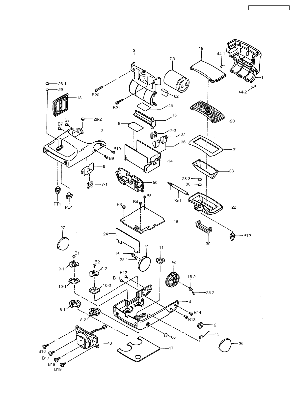
10 EXPLODED VIEWS
10.1. FRAME & CASING SECTION
DMW-FL28PP / DMW-FL28E
29
Page 30

DMW-FL28PP / DMW-FL28E
10.2. PACKING PARTS & ACCESSORIES SECTION
30
Page 31

11 REPLACEMENT PARTS LIST
DMW-FL28PP / DMW-FL28E
11.1. MECHANICAL REPLACEMENT
PARTS LIST
11.1.1. FRAME & CASING SECTION
PARTS LIST
Ref.
No.
1 SS094-98 MAIN CASE (A)
2 SS094-99 MAIN CASE (B)
3 SS095-40 MAIN CASE (C)
4 SS094-97 MAIN CASE (D)
5 SS806-74 BATTERY SEAL
6 SS209-73S BATTERY TERMINAL
7-1 SS040-03 TERMINAL GUARD
7-2 SS040-03 TERMINAL GUARD
8-1 SS058-58 DIAL KNOB
8-2 SS058-58 DIAL KNOB
9-1 SS162-08 DIAL BRUSH TERMINAL
9-2 SS162-08 DIAL BRUSH TERMINAL
10-1 SS162-09 CLICK SPRING
10-2 SS162-09 CLICK SPRING
11 ES011-61 FLASH BUTTON
12 SS203-01 JACK MOLD
13 SS166-15 JACK SPRING
14 SS027-66 BATTERY CASE
15 SS029-09 BATTERY SEPARATOR
16-1 SS038-74 CLICK MOLD
16-2 SS038-74 CLICK MOLD
17 SS222-93 BACK PLATE
18 SS001-69 BATTERY LID UNIT
19 SS056-90 FRONT PANEL
20 SS056-91 FRESNEL PANEL
21 SS228-35 ORNAMENT PLATE
22 SS040-04 REFLECTION UMBRELLA COVER
24 SS800-96 INSULATION SHEET
25-1 SS164-35 SPRING
25-2 SS164-35 SPRING
26 SS024-93 SIDE RUBBER 1
27 SS024-94 SIDE RUBBER 2
28-1 SS022-16 PROTECTION PLATE
28-2 SS022-16 PROTECTION PLATE
28-3 SS022-16 PROTECTION PLATE
29 SS025-13 ND FILTER (0.3)
30 SS025-04 ND FILTER (0.4) (Refer to
36 SS209-71S BATTERY TERMINAL (+)
37 SS209-72 BATTERY TERMINAL (-)
38 SS014-13 REFLECTION UMBRELLA
39 SS011-77 XE BUSHING
41 SS013-57 BOUNCE SHAFT (A)
42 SS013-58 BOUNCE SHAFT (B)
43 SS128-84 SHOE UNIT
44-1 SS166-16 LOCK SPRING
44-2 SS166-16 LOCK SPRING
45 SS804-11 SEAL
Part No. Part Name & Description Remarks
Adjustment
SS025-12 ND FILTER (0.5) (Refer to
SS025-08 ND FILTER (0.6) (Refer to
Procedures)
Adjustment
Procedures)
Adjustment
Procedures)
Ref.
No.
49 SS306-89 C.B.A. (A) (RTL)
50 SS306-90 C.B.A. (B) (RTL)
60 SS228-41 SYNC PLATE
62 SG900-29 CUSHION
B1 SG012-70 SCREW
B2 SG012-70 SCREW
B3 SG022-83 SCREW
B4 SG022-83 SCREW
B5 SG022-83 SCREW
B7 SG052-35 SCREW
B8 SG052-35 SCREW
B9 SG052-35 SCREW
B10 SG052-35 SCREW
B11 SG052-35 SCREW
B12 SG052-35 SCREW
B13 SG052-35 SCREW
B14 SG052-35 SCREW
B16 SG052-34 SCREW
B17 SG052-34 SCREW
B18 SG052-34 SCREW
B19 SG052-34 SCREW
B20 SG022-60 SCREW
B21 SG022-60 SCREW
Part No. Part Name & Description Remarks
11.1.2. PACKING PARTS & ACCESSORIES
SECTION PARTS LIST
Ref.
No.
101 SP500-63 POLY BAG
102 SP500-33 POLY BAG
103 SP500-33 POLY BAG
104 SP603-67 INSTRUCTION BOOK
104 SP603-68 INSTRUCTION BOOK
105 SP012-21 PACKING CASE
106 SP400-35 PAD
107 SS056-92 WIDE PANEL
Part No. Part Name & Description Remarks
DMW-FL28PP
DMW-FL28E
31
Page 32

DMW-FL28PP / DMW-FL28E
11.2. ELECTRICAL REPLACEMENT
PARTS LIST
Ref.
No.
C1 SC100-07 E.CAPACITOR CH 10V 220U
C3 SS505-78 E.CAPACITOR CH 330V 800U
C4 SC201-22 C.CAPACITOR CH 250V0.047U
C6 SC201-27 T.CAPACITOR CH 16V 2.2U
C7 ECJ2XB1H473K C.CAPACITOR CH 50V 0.047U
C8 ECJ2XB1H823K C.CAPACITOR CH 50V 0.082U
C9 SC201-24 C.CAPACITOR CH 50V 0.15U
C10 SC002-22 C.CAPACITOR CH 50V 220P
C11 SC002-22 C.CAPACITOR CH 50V 220P
C12 ECJ2VB1H223K C.CAPACITOR CH 50V 0.022U
C13 ECJ2VB1H103K C.CAPACITOR CH 50V 0.01U
C14 SC102-51 CAPACITOR CH 400V 0.047U
C15 SC102-51 CAPACITOR CH 400V 0.047U
C16 ECJ2XB1H473K C.CAPACITOR CH 50V 0.047U
C17 F3K1C1050001 T.CAPACITOR CH 16V 1U
C18 SC201-27 T.CAPACITOR CH 16V 2.2U
C19 F3K1C1050001 T.CAPACITOR CH 16V 1U
C20 SC201-25 C.CAPACITOR CH 25V 3300P
C21 ECJ2VB1H393K C.CAPACITOR CH 50V 0.039U
C22 F3K1A4750002 T.CAPACITOR CH 10V 4.7U
C23 ECEA1CKS101 E.CAPACITOR 16V 100U
C24 SC201-26 C.CAPACITOR CH 25V 0.01U
C25 SC201-26 C.CAPACITOR CH 25V 0.01U
CUT1 SC014-06 FUSE
CUT2 SC014-12 FUSE
D1 MA2J11100L DIODE
D2 SC105-24 DIODE
D3 MA2J11100L DIODE
D4 SC105-25 DIODE
D5 SC105-20 DIODE
D6 RB501V-40 DIODE
D7 MA2J11100L DIODE
D8 MA2J11100L DIODE
D9 MA2J11100L DIODE
D10 MA2J11100L DIODE
IC1 SS534-23 IC
IC2 NJM2903V IC C0BBBA000032
IC3 NJM2904M IC C0ABBA000021
IC4 TC7W00F IC
IT1 SC013-53 IGBT
LD1 SC125-09 LED
LD2 SC125-10 LED
PD1 SS512-34S PHOTO DIODE
PT1 SS512-18 PHOTO TRANSISTOR
PT2 SS512-08 PHOTO TRANSISTOR
Q1 SC013-01 TRANSISTOR
Q2 SC013-01 TRANSISTOR
Q3 SC013-49 TRANSISTOR
Q4 SC013-51 TRANSISTOR
Q5 SC013-51 TRANSISTOR
Q6 SC013-52 TRANSISTOR
Q7 SC013-51 TRANSISTOR
Q8 SC013-39 TRANSISTOR
Q9 SC013-39 TRANSISTOR
Part No. Part Name & Description Remarks
Ref.
No.
Q10 SC013-39 TRANSISTOR
Q11 SC013-51 TRANSISTOR
R1 ERJ3GEYJ103V M.RESISTOR CH 1/10W 10K D0GB103JA002
R2 ERJ3GEYJ103V M.RESISTOR CH 1/10W 10K D0GB103JA002
R3 ERJ3GEYJ152V M.RESISTOR CH 1/10W 1.5K
R4 ERJ3GEYJ821 M.RESISTOR CH 1/10W 820
R5 SC207-85 M.RESISTOR CH 1/4W 1.2M
R6 SC207-85 M.RESISTOR CH 1/4W 1.2M
R7 ERJ6GEYJ125 M.RESISTOR CH 1/10W 1.2M
R8 ERJ6GEYJ125 M.RESISTOR CH 1/10W 1.2M
R9 ERJ6GEYG222 M.RESISTOR CH 1/10W 2.2K
R10 ERJ3GEYJ333 M.RESISTOR CH 1/10W 33K
R11 ERJ3GEYJ683 M.RESISTOR CH 1/10W 68K
R12 ERJ3GEYJ105V M.RESISTOR CH 1/10W 1M
R13 ERJ3GEYJ103V M.RESISTOR CH 1/10W 10K D0GB103JA002
R14 ERJ3GEYJ103V M.RESISTOR CH 1/10W 10K D0GB103JA002
R15 ERJ3GEYJ222 M.RESISTOR CH 1/10W 2.2K
R16 ERJ3GEYJ332 M.RESISTOR CH 1/10W 3.3K
R17 ERJ3GEYJ222 M.RESISTOR CH 1/10W 2.2K
R18 ERJ6GEYJ474 M.RESISTOR CH 1/10W 470K
R19 ERJ6GEYJ474 M.RESISTOR CH 1/10W 470K
R20 ERDS2TJ333J C.RESISTOR CH 1/4W 33K
R21 ERJ6GEYG330 M.RESISTOR CH 1/8W 33
R22 ERDS2FJ330 C.RESISTOR 1/4W 33
R23 ERJ8GEYJ155 M.RESISTOR CH 1/4W 1.5M
R25 ERJ3GEYJ102V M.RESISTOR CH 1/10W 1K
R26 ERJ3GEYJ561 M.RESISTOR CH 1/10W 560
R27 ERJ3GEYJ472 M.RESISTOR CH 1/10W 4.7K
R28 ERJ3GEYJ222 M.RESISTOR CH 1/10W 2.2K
R29 ERJ3GEYJ184V M.RESISTOR CH 1/10W 180K
R30 ERJ3GEYJ102V M.RESISTOR CH 1/10W 1K
R31 ERJ3GEYJ273 M.RESISTOR CH 1/10W 27K
R32 SC207-86 M.RESISTOR CH 1/10W 11.5K
R33 SC207-87 M.RESISTOR CH 1/10W 24.3K
R34 ERJ3GEYJ202 M.RESISTOR CH 1/10W 2K
R35 ERJ3GEYJ103V M.RESISTOR CH 1/10W 10K D0GB103JA002
R36 ERJ6GEYJ474 M.RESISTOR CH 1/10W 470K
R37 ERJ3GEYJ473V M.RESISTOR CH 1/10W 47K D0GB473JA002
R38 ERJ3GEYJ105V M.RESISTOR CH 1/10W 1M
R39 ERJ3GEYD153V M.RESISTOR CH 1/10W 15K D0HB153ZA002
R40 ERJ6GEYG103 M.RESISTOR CH 1/10W 10K
R41 ERJ3GEYJ684 M.RESISTOR CH 1/10W 680K D0GB684JA002
R42 ERJ3GEYJ223 M.RESISTOR CH 1/10W 22K
R43 ERJ3GEYJ223 M.RESISTOR CH 1/10W 22K
R44 ERJ3GEYJ102V M.RESISTOR CH 1/10W 1K
R45 ERJ3GEYJ103V M.RESISTOR CH 1/10W 10K D0GB103JA002
R46 ERJ3GEYJ103V M.RESISTOR CH 1/10W 10K D0GB103JA002
R48 ERJ3GEYJ103V M.RESISTOR CH 1/10W 10K D0GB103JA002
R49 ERJ3GEYJ684 M.RESISTOR CH 1/10W 680K D0GB684JA002
R50 ERJ6GEYJ220 M.RESISTOR CH 1/10W 22
R51 ERJ3GEYJ204 M.RESISTOR CH 1/10W 200K
R53 ERJ6GEYG331 M.RESISTOR CH 1/10W 330
R55 ERJ3GEYJ102V M.RESISTOR CH 1/10W 1K
R56 ERJ3GEYJ220 M.RESISTOR CH 1/10W 22
R57 ERJ3GEYJ103V M.RESISTOR CH 1/10W 10K D0GB103JA002
RQ1 DTA143XU DIGITAL TRANSISTOR
RQ2 SC032-71 DIGITAL TRANSISTOR
RQ3 DTC124XU DIGITAL TRANSISTOR
RQ4 SC032-79 DIGITAL TRANSISTOR
RQ5 DTA114EUA106 DIGITAL TRANSISTOR
RQ6 DTC124XU DIGITAL TRANSISTOR
RQ7 DTC124XU DIGITAL TRANSISTOR
RQ8 DTC114EU DIGITAL TRANSISTOR
SCR1 SC023-52 THYRISTOR
SCR2 SC023-52 THYRISTOR
T1 SS516-60 TRANSFORMER
T2 SS508-60 TRIGGER COIL
TH1 SC010-15 THERMISTOR
Part No. Part Name & Description Remarks
32
Page 33

DMW-FL28PP / DMW-FL28E
Ref.
No.
TH2 SC010-16 THERMISTOR
VR1 SC065-78 VARIABLE RESISTOR
VR2 SC065-79 VARIABLE RESISTOR
VR3 SC065-80 VARIABLE RESISTOR
XE1 SS501-50 XE TUBE
ZD1 MA3270M DIODE MAZ32700M
Part No. Part Name & Description Remarks
33
Page 34

DMW-FL28PP / DMW-FL28E
12 SCHEMATIC DIAGRAM FOR PRINTING WITH A4 SIZE
34
Page 35

7 SCHEMATIC DIAGRAMS
2
1
DMW-FL28PP / DMW-FL28E
H
Q1
T1
Q2
RQ1
R1 10K
D2
W4
W10
R7 1.2MR8 1.2M
C4 0.047
R4 820
C3 800
G
(OSC)
F
AUTO
C-AUTO
MANUAL
SLAVE
R2 10K
OFF
R3 1.5K
Q3
SW1-1
D1
(+12V)
(VBATT)
RQ2
CUT1
E
C1 10V 220
CUT2
10K
10K
(OSCS)
R53 330
W8
1.5V x4
W7
D
W1
(GND1)
R5 1.2M
R6 1.2M
8V
R9 22KR10 33K
R11 68K
Q4
W14
PT1
C6 16V 2.2
OFF
R12 1M
C10 220P
W13
SW1-2
C7 0.047
R56 22
W11
W12
MANUAL
C-AUTO
AUTO
C8 0.082
4
5.6
2.8
SW2-1
PT2
SLAVE
C9 0.15
SW2-
FULL
C11 220P
TH1
VR1
RQ3
1/4
TH2
VR2
100K
22K
47K
RQ5
10K
R30 1K
LD1
10K
C
D6
IC1
IC2
1
2
3
4
B
C23 10V 100
C18 16V 2.2
C24 0.01
C19 16V 1
R31 27K
R34 2KR35 10K
R32 11.5K
8
7
6
5
VR3
R33 24.3K
C25 0.01
A
R36 470K
R51 200K
R37 47K
C20 3300P
Q9
Q8
W9
W9
C21 0.039
PD1
R39 15K
D7
R38 1M
R4
R40 10K
R42
35
Page 36

C12
0.022
DMW-FL28PP / DMW-FL28E
W6
Q7
SCR2
R23 1.5M
280V
D10
(TG)
R25 1K
C16 0.047
R26 560
SW3
R27 4.7K
R28 2.2K
D5
RQ4
2.2K
47K
W3
T2
W2
XE1
C14 0.047
R18 470K
R57 10K
R13 10K
Q5
R19 470K
R22 33
D4
(STP)
C15 0.047
W5
R20 33K
R14 10K
R15 2.2K
SCR1
IT1
R16 3.3K
Q6
R21 33
D3
R17 2.2K
ZD1
C13 0.01
R29 180K
5V
C17 16V 1
W15
W16
IC3
Q10
D9
R46 10K
C26 1000P
RQ7
22K
47K
R48 10K
R55 1K
RQ8
LD2
R50 220
10K
10K
IC4
1
2
3
4
8
7
6
5
R49 680K
Q11
C22 10V 4.7
1
2
3
4
8
7
6
5
RQ6
R44 1K
22K
47K
R45 10K
36
 Loading...