

Page 1
ORDER NO. DSD1205012CE
Blu-ray Disc Player
Model No. DMP-BBT01EB
DMP-BBT01EG
Colour
(K)...........Black Type
© Panasonic Corporation 2012 Unauthorized copying and distribution is a violation of law.
Page 2

TABLE OF CONTENTS
PAG E PAG E
1 Safety Precautions -----------------------------------------------3
1.1. General Guidelines ----------------------------------------3
1.2. Leakage Current Cold Check ---------------------------3
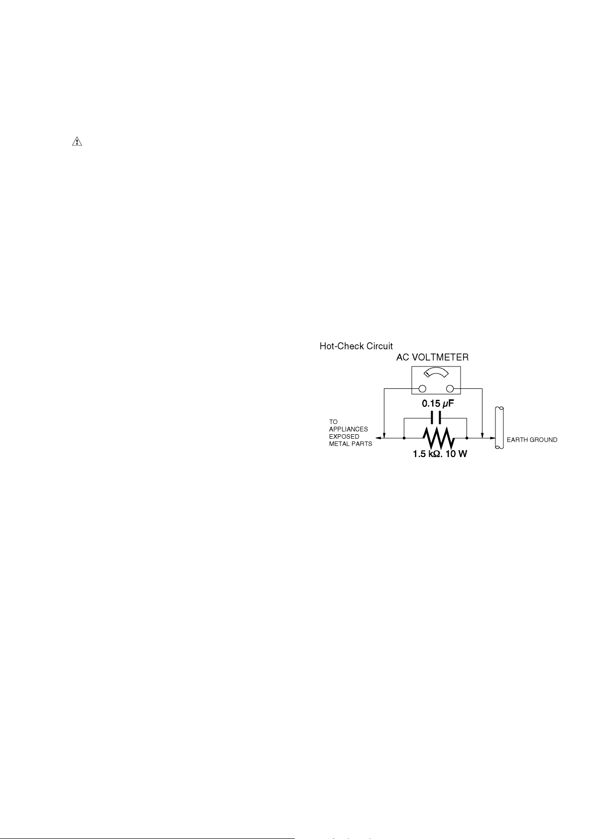
1.3. Leakage Current Hot Check (See Figure 1.) --------3
2Warning--------------------------------------------------------------4
2.1. Prevention of Electrostatic Discharge (ESD)
to Electrostatically Sensitive (ES) Devices ----------4
2.2. Caution for AC Cord (For EB)---------------------------5
2.3. Precaution of Laser Diode -------------------------------6
2.4. Service Caution Based On Legal Restrictions ------ 7
2.5. Static Electricity Protection Measures ----------------8
2.6. Ground for electrostatic breakdown
prevention----------------------------------------------------8
3 Service Navigation------------------------------------------------9
3.1. Service Infomation -----------------------------------------9
3.2. Caution for DivX ------------------------------------------ 10
4 Specifications ---------------------------------------------------- 11
4.1. Others (Licenses) ---------------------------------------- 12
5 Location of Controls and Components------------------ 14
6 Operating Instructions ---------------------------------------- 17
6.1. Taking out the Disc from Drive Unit when the
Disc cannot be ejected by [Eject] switch ----------- 17
7 Multiple Pressing Function ---------------------------------- 18
7.1. About the Multiple Pressing of the Unit’s
Remote Control------------------------------------------- 18
7.2. How to enter the Special Modes using the
Multiple Pressing Function of the Unit’s
Remote Control------------------------------------------- 18
8 Service Mode ----------------------------------------------------- 24
8.1. About the Service Mode -------------------------------- 24
8.2. Service Mode List ---------------------------------------- 25
8.3. Self-Diagnostics Functions ---------------------------- 29
9 Service Fixture & Tools --------------------------------------- 32
10 Disassembly and Assembly Instructions --------------- 33
10.1. Unit----------------------------------------------------------- 33
10.2. Drive Unit--------------------------------------------------- 38
11 Measurements and Adjustments -------------------------- 41
11.1. Service Positions ----------------------------------------- 41
11.2. Adjustment of Drive Unit/BD Digital P.C.B. -------- 42
11.3. Caution for Replacing Parts --------------------------- 45
12 Block Diagram --------------------------------------------------- 46
12.1. Overall Block Diagram ---------------------------------- 46
12.2. Input Digi-Net P.C.B. Regulator Circuit Block
Diagram----------------------------------------------------- 47
12.3. BD Digital P.C.B. Regulator Circuit Block
Diagram----------------------------------------------------- 48
12.4. Digital Video/Audio Circuit Block Diagram --------- 49
12.5. Digital (Front End Section) Circuit Block
Diagram----------------------------------------------------- 50
12.6. Digital (Back End Section [1]) Circuit Block
Diagram----------------------------------------------------- 51
12.7. Digital (Back End Section [2]) Circuit Block
Diagram----------------------------------------------------- 52
13 Wiring Connection Diagram --------------------------------- 53
13.1. Interconnection Diagram ------------------------------- 53
2
Page 3
1 Safety Precautions
1.1. General Guidelines
1. IMPORTANT SAFETY NOTICE
There are special components used in this equipment
which are important for safety. These parts are marked by
in the Schematic Diagrams, Circuit Board Layout,
Exploded Views and Replacement Parts List. It is essential that these critical parts should be replaced with manufacturer’s specified parts to prevent X-RADIATION,
shock, fire, or other hazards. Do not modify the original
design without permission of manufacturer.
2. An Isolation Transformer should always be used during
the servicing of AC Adaptor whose chassis is not isolated
from the AC power line. Use a transformer of adequate
power rating as this protects the technician from accidents resulting in personal injury from electrical shocks. It
will also protect AC Adaptor from being damaged by accidental shorting that may occur during servicing.
3. When servicing, observe the original lead dress. If a short
circuit is found, replace all parts which have been overheated or damaged by the short circuit.
4. After servicing, see to it that all the protective devices
such as insulation barriers, insulation papers shields are
properly installed.
5. After servicing, make the following leakage current
checks to prevent the customer from being exposed to
shock hazards.
1.3. Leakage Current Hot Check (See Figure 1.)
1. Plug the AC cord directly into the AC outlet. Do not use
an isolation transformer for this check.
2. Connect a 1.5 kΩ, 10 W resistor, in parallel with a 0.15 μF
capacitor, between each exposed metallic part on the set
and a good earth ground, as shown in Figure 1.
3. Use an AC voltmeter, with 1 kΩ/V or more sensitivity, to
measure the potential across the resistor.
4. Check each exposed metallic part, and measure the voltage at each point.
5. Reverse the AC plug in the AC outlet and repeat each of
the above measurements.
6. The potential at any point should not exceed 0.75 V RMS.
A leakage current tester (Simpson Model 229 or equivalent) may be used to make the hot checks, leakage current must not exceed 1/2 mA. In case a measurement is
outside of the limits specified, there is a possibility of a
shock hazard, and the equipment should be repaired and
rechecked before it is returned to the customer.
1.2. Leakage Current Cold Check
1. Unplug the AC cord and connect a jumper between the
two prongs on the plug.
2. Measure the resistance value, with an ohmmeter,
between the jumpered AC plug and each exposed metallic cabinet part on the equipment such as screwheads,
connectors, control shafts, etc. When the exposed metallic part has a return path to the chassis, the reading
should be between 1 MΩ and 5.2 MΩ. When the exposed
metal does not have a return path to the chassis, the
reading must be infinity.
Figure. 1
3
Page 4

2Warning
2.1. Prevention of Electrostatic Discharge (ESD) to Electrostatically Sensitive (ES) Devices
Some semiconductor (solid state) devices can be damaged easily by static electricity. Such components commonly are called Electrostatically Sensitive (ES) Devices.
The following techniques should be used to help reduce the incidence of component damage caused by electrostatic discharge
(ESD).
1. Immediately before handling any semiconductor component or semiconductor-equipped assembly, drain off any ESD on your
body by touching a known earth ground. Alternatively, obtain and wear a commercially available discharging ESD wrist strap,
which should be removed for potential shock reasons prior to applying power to the unit under test.
2. After removing an electrical assembly equipped with ES devices, place the assembly on a conductive surface such as aluminum foil, to prevent electrostatic charge buildup or exposure of the assembly.
3. Use only a grounded-tip soldering iron to solder or unsolder ES devices.
4. Use only an antistatic solder removal device. Some solder removal devices not classified as "antistatic (ESD protected)" can
generate electrical charge sufficient to damage ES devices.
5. Do not use freon-propelled chemicals. These can generate electrical charges sufficient to damage ES devices.
6. Do not remove a replacement ES device from its protective package until immediately before you are ready to install it. (Most
replacement ES devices are packaged with leads electrically shorted together by conductive foam, aluminum foil or comparable conductive material).
7. Immediately before removing the protective material from the leads of a replacement ES device, touch the protective material
to the chassis or circuit assembly into which the device will be installed.
CAUTION :
Be sure no power is applied to the chassis or circuit, and observe all other safety precautions.
8. Minimize bodily motions when handling unpackaged replacement ES devices. (Otherwise harmless motion such as the
brushing together of your clothes fabric or the lifting of your foot from a carpeted floor can generate static electricity (ESD) sufficient to damage an ES device).
4
Page 5
2.2. Caution for AC Cord (For EB)
2.2.1. Information for Your Safety
IMPORTANT
Your attention is drawn to the fact that recording of prerecorded tapes or discs or other published or broadcast
material may infringe copyright laws.
WARNING
To reduce the risk of fire or shock hazard, do not expose
this equipment to rain or moisture.
CAUTION
To reduce the risk of fire or shock hazard and annoying
interference, use the recommended accessories only.
FOR YOUR SAFETY
DO NOT REMOVE THE OUTER COVER
To prevent electric shock, do not remove the cover. No user
serviceable parts inside. Refer servicing to qualified service
personnel.
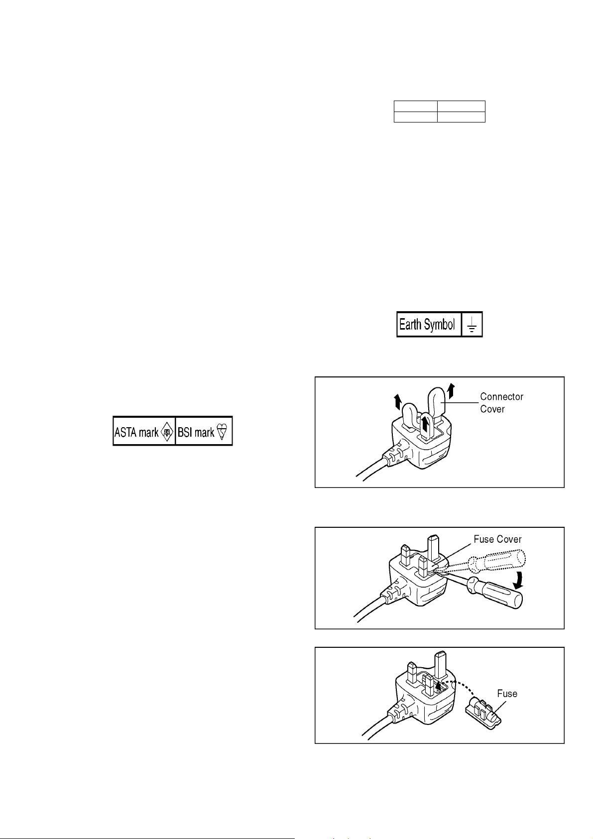
2.2.2. Caution for AC Mains Lead
For your safety, please read the following text carefully.
This appliance is supplied with a moulded three-pin mains plug
for your safety and convenience.
A 5-ampere fuse is fitted in this plug.
Should the fuse need to be replaced please ensure that the
replacement fuse has a rating of 5 amperes and it is approved
by ASTA or BSI to BS1362
Check for the ASTA mark or the BSI mark on the body of the
fuse.
2.2.2.1. Important
The wires in this mains lead are coloured in accordance with
the following code:
Blue Neutral
Brown Live
As the colours of the wires in the mains lead of this appliance
may not correspond with the coloured markings identifying the
terminals in your plug, proceed as follows:
The wire which is coloured BLUE must be connected to the terminal in the plug which is marked with the letter N or coloured
BLACK.
The wire which is coloured BROWN must be connected to the
terminal in the plug which is marked with the letter L or coloured
RED.
Under no circumstances should either of these wires be connected to the earth terminal of the three pin plug, marked with
the letter E or the Earth Symbol.
2.2.2.2. Before Use
Remove the Connector Cover as follows.
If the plug contains a removable fuse cover you must ensure
that it is refitted when the fuse is replaced.
If you lose the fuse cover, the plug must not be used until a
replacement cover is obtained.
A replacement fuse cover can be purchased from your local
Panasonic Dealer.
If the fitted moulded plug is unsuitable for the socket outlet in
your home then the fuse should be removed and the plug cut
off and disposed of safety.
There is a danger of severe electrical shock if the cut off plug is
inserted into any 13-ampere socket.
If a new plug is to be fitted please observe the wiring code as
shown below.
If in any doubt, please consult a qualified electrician.
2.2.2.3. How to Replace the Fuse
1. Remove the Fuse Cover with a screwdriver.
2. Replace the fuse and attach the Fuse cover.
5
Page 6
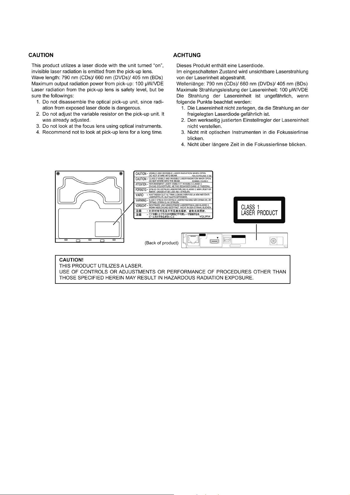
2.3. Precaution of Laser Diode
6
Page 7

2.4. Service Caution Based On Legal Restrictions
This service manual contains technical information, which allow service personnel’s to understand and service this model.
Please place orders using the parts list and not the drawing reference numbers.
If the circuit is changed or modified, the information will be followed by service manual to be controlled with original service manual.
2.4.1. General Description About Lead Free Solder (PbF)
The lead free solder has been used in the mounting process of all electrical components on the printed circuit boards used for this
equipment in considering the globally environmental conservation.
The normal solder is the alloy of tin (Sn) and lead (Pb). On the other hand, the lead free solder is the alloy mainly consists of tin
(Sn), silver (Ag) and Copper (Cu), and the melting point of the lead free solder is higher approx.30°C (86°F) more than that of the
normal solder.
Distinction of P.C.B. Lead Free Solder being used
Service caution for repair work using Lead Free Solder (PbF)
• The lead free solder has to be used when repairing the equipment for which the lead free solder is used.
(Definition: The letter of “PbF” is printed on the P.C.B. using the lead free solder.)
• To put lead free solder, it should be well molten and mixed with the original lead free solder.
• Remove the remaining lead free solder on the P.C.B. cleanly for soldering of the new IC.
• Since the melting point of the lead free solder is higher than that of the normal lead solder, it takes the longer time to melt the
lead free solder.
• Use the soldering iron (more than 70W) equipped with the temperature control after setting the temperature at 350±30°C
(662±86°F).
Recommended Lead Free Solder (Service Parts Route.)
• The following 3 types of lead free solder are available through the service parts route.
RFKZ03D01KS-----------(0.3mm 100g Reel)
RFKZ06D01KS-----------(0.6mm 100g Reel)
RFKZ10D01KS-----------(1.0mm 100g Reel)
Note
* Ingredient: tin (Sn) 96.5%, silver (Ag) 3.0%, Copper (Cu) 0.5%, Cobalt (Co) / Germanium (Ge) 0.1 to 0.3%
7
Page 8
2.5. Static Electricity Protection Measures
• The laser diode in the traverse unit (optical pick-up) may break down due to potential difference caused by static electricity of
clothes or human body.
So, be careful of electrostatic breakdown during repair of the traverse unit (optical pick-up).
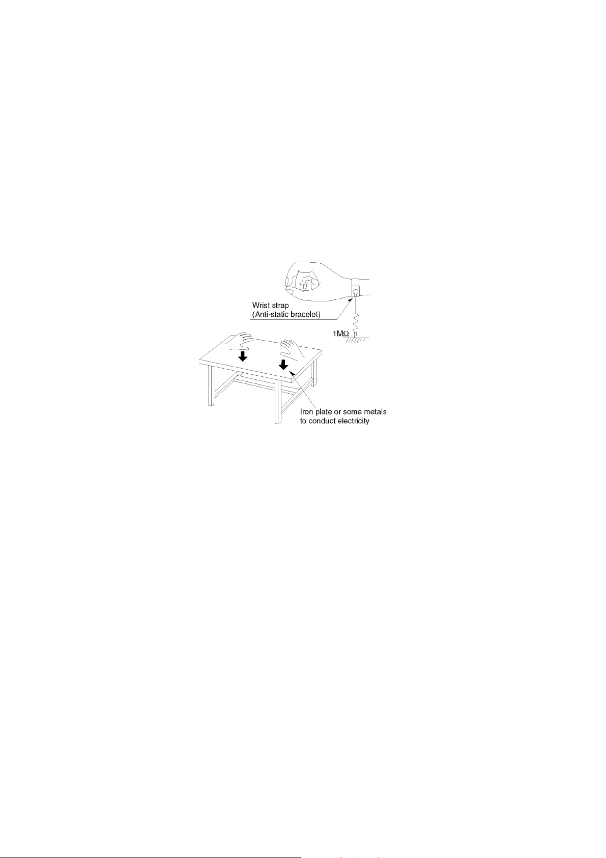
2.6. Ground for electrostatic breakdown prevention
• As for parts that use optical pick-up (laser diode), the optical pick-up is destroyed by the static electricity of the working environment.
Repair in the working environment that is grounded.
2.6.1. Work table grounding
• Put a conductive material (sheet) or steel sheet on the area where the traverse unit (optical pick-up) is placed, and ground the
sheet.
2.6.2. Human body grounding
• Use the anti-static wrist strap to discharge the static electricity from your body.
2.6.3. When exchange the BDP Drive
• Before remove the ESD prevention bag, make sure to use the anti-static wrist strap to discharge the static electricity when
replace the BDP Drive.
Note:
The ESD prevention bag is used to replace the original short-circuit point.
It can be removed while placing the BDP Drive.
8
Page 9

3 Service Navigation
3.1. Service Infomation
This service manual contains technical information which will allow service personnel’s to understand and service this model.
Please place orders using the parts list and not the drawing reference numbers.
If the circuit is changed or modified, this information will be followed by supplement service manual to be filed with original service
manual.
1. This service manual does not contain the following information, because of the impossibility of servicing at component level.
• Schematic Diagram, Block Diagram and P.C.B. layout of BD Digital P.C.B..
• Parts List for individual parts of BD Digital P.C.B..
• Exploded View and Parts List for individual parts of Drive Unit.
2. The following category are recycle module part. Please send them to Central Repair Center.
• BD Digital P.C.B. (DMP-BBT01EB: RFKB76275DBT)
• BD Digital P.C.B. (DMP-BBT01EG: RFKB76275CGT)
• Drive Unit: VXY2162
9
Page 10
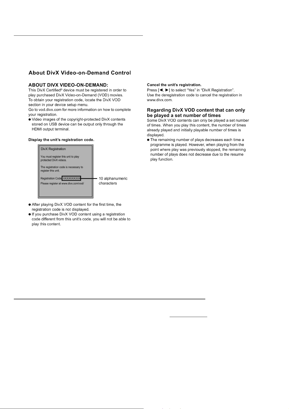
3.2. Caution for DivX
“Warning for Customers Who Use DivX Video-on-Demand content” when replacing the FLASH ROM or EEPROM or P.C.B.
First, copy the Last part of this page for the customers who continue to use DivX Video-on-Demand service.
Appendix:
*Parts that memorize user’s information are only FLASH ROM.
*The registration of Registration Code is possible for half a year up to 6 recorders up to 10 recorders a year.
Registration Code is memorized in FLASH ROM (BD Digital P.C.B.).
If exchange above P.C.B. or FLASH ROM, new registration Code differ from previous Registration Code will be generated.
In this case if your customer uses DivX Video-on-Demand service, he/she will no longer be able to play any content that he/she purchased under that same registration code.
Therefore your customer will need to obtain and register the new registration code.
*Copy this page and cut on the dotted line and give the lower half to your customer.
- - - - - - - - - - - - - - - - - - - - - - - - - - - - - - - - - - - - - - - - - - - - - - - - - - - - - - - - - - - - - - - - - - - - - - - - - - - - - - - - - - - - - - - - - - - - - - -
Warning for Customers Who Use the DivX Video-on-Demand content.
1. The registration code has been changed for the repair of the product or the product exchange.
2. Obtain and register a new registration code, otherwise you will no longer be able to play DivX Video-on-Demand content.
3. Follow the procedure on the DivX Video-on-Demand web site to register at http://vod.divx.com/
*If you do not use the DivX Video-on-Demand content, please ignore this warning.
.
10
Page 11

4 Specifications
Power supply: DC 12V (DC IN terminal)
Power consumption: Approx. 8.9 W
In standby mode: Approx. 0.5 W
In quick start standby mode: Approx. 4 W
Operating temperature range: +5°C to +35°C
Operating humidity range: 10 % to 80 % RH (no condensation)
Signal system: PAL /NTS C
Digital audio output:
Optical digital output: Optical terminal
HDMI AV output:
Output connector: TypeA (19 pin): 1 system
480p (525p) / 576p (625p) /
1080i (1125i) / 720p (750p) /
1080p (1125p)
HDMI (V.1.4a with 3D, Content
Type) This unit supports “HDAVI
Control5” function.
SD card slot:
Connector: 1 system
USB slot:
USB2.0: 1 system
Ethernet:
10BASE-T/100BASE-TX: 1 system
Wireless LAN:
Antenna: Tx 1, Rx 1+diversity
Standard Compliance: IEEE802.11n / IEEE802.11g /
IEEE802.11b
Transmission system: OFDM system, DSSS system
Frequency Range: 2.4GHz band
Transfer rate (standard): IEEE802.11n: Max 150Mbps
* Transfer rates are
theoretial values; however,
actual communication rate
will vary according to
communication
environment or connected
equipment.
Access Mode: Infrastructure mode
Security: WPA™/WPA2™
Optical pick-up: System with 2 lenses
Wave length: 790 nm (CDs)/660 nm (DVDs)/
LASER Specification
Class 1 LASER Product:
Wave length: 790 nm (CDs)/660 nm (DVDs)/
Laser power: No hazardous radiation is emitted
Region management
information:
DVD-Video: region number “2” or “ALL”
BD-Video: region code “B”
Media:
Playable disc:
BD-Video
(Blu-Ray 3D, BD-LIVE):
BD-RE: Version3 (Single Layer / Dual
BD-R: Version2 (Single Layer / Dual
DVD-R/DVD-R DL:
IEEE802.11g: Max 54Mbps
IEEE802.11b: Max 11Mbps
(Encryption type: TKIP/AES,
Authentication type: PSK)
WEP(64bit/128bit)
405 nm (BDs)
405 nm (BDs)
with the safety protection
BD-ROM Version 2.4
Layer), JPEG, MPO
Layer), DivX
DVD-Video format*
®
, MKV
1
,
DVD Video Recording format*
1
AVCHD format*
, DivX®, JPEG,
MPO, FLAC, MP3, MKV, WAV
1
,
DVD-RW:
+R/+RW/+R DL:
DVD-Video format*
DVD Video Recording format*
AVCHD format*
1
, AVCHD format*
Video*
1
,
1
1
,
1
DVD-Video: DVD-Video format
CD-Audio: CD-DA
CD-R/CD-RW: CD-DA, JPEG, MPO, FLAC, MP3,
®
, MKV, WAV
DivX
*1 Finalizing is necessary.
USB device:
USB Standard: USB 2.0 High Speed
®
MP4,MPEG, DivX
, MKV, JPEG,
MPO, FLAC, MP3, WAV
Format: FAT12, FAT16, FAT32, NTFS
SD card:
SD Memory Card*
Format:
2
JPEG, MPO, AVCHD, AVCHD 3D,
MPEG-2
FAT12, FAT16, FAT32
*3
, exFAT
*4
*2 support SDHC, SDXC card
support miniSD
support microSD
(need a microSD
TM
Cards (need a miniSDTM Adaptor.)
TM
/microSDHC/microSDXC Cards
TM
Adaptor.)
*3 Not support long file name
*4 SDXC only
Contents:
JPEG:
(CD-R/CD-RW, DVD-R/DVD-R DL, BD-RE, USB device, SD card)
File format: JPEG
(Motion JPEG and Progressive
JPEG are not supported.)
Pixcels: 34 x 34 to 8192 x 8192
Sub sampling: 4:2:2, 4:2:0
MP3:
(CD-R/CD-RW, DVD-R/DVD-R DL, USB device)
File format: MP3
Compression rate: 32kbps to
320kbps
Sampling rate: 44.1kHz, 48kHz
®
DivX
(CD-R/CD-RW, DVD-R/DVD-R DL, BD-R, USB device)
File format: DivX, DivX HD
(DivX Plus HD is not supported.)
MKV:
(CD-R/CD-RW, DVD-R/DVD-R DL, BD-R, USB device)
File format: MKV
FLAC:
(CD-R/CD-RW, DVD-R/DVD-R DL, USB device)
File format: FLAC
Maximum sampling rate: 192 kHz/24 bit
WAV:
(CD-R/CD-RW, DVD-R/DVD-R DL, USB device)
File format: WAV
Maximum sampling rate: 48 kHz/16 bit
AVCHD (H.264):
(DVD-R/DVD-R DL, DVD-RW, +R/+RW/+R DL, SD card)
File format: AVCHD format V2.0
Dimensions: 179mm(W) x 27mm(H) x 180mm(D)
(including the projecting parts, Horizontal instlation with no pedestal.)
235mm(W) x 95mm(H) x 250mm(D)
(including the projecting parts, Horizontal diagonal instlation with pedestal.)
Mass: Approx. 0.9 kg
Approx. 1.0 kg (induding pedestal)
Solder: This model uses lead free solder
(PbF).
11
Page 12

AC Adaptor Power Source: 100V to 240V,
50/60Hz
Power consumption: 42 W
DC output: DC 12 V, 2500 mA
Note: Specifications are subject to change
without notice.
4.1. Others (Licenses)
12
Page 13
13
Page 14
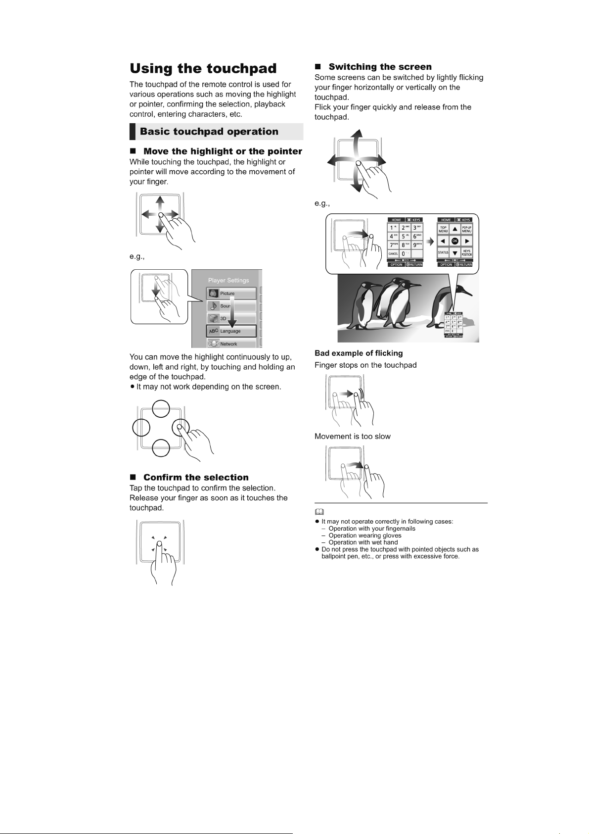
5 Location of Controls and Components
1 Turn the unit on and off
2 Show the Home screen of the VIERA
Connect
3 Show HOME menu
4 Touchpad
Used for various operation
Move the highlight, confirm the selection, etc.
5 Show Option menu
6 Coloured buttons (red, green, yellow, blue)
Used for various purposes depending on the
display
7 Show NETFLIX screen
8 Start up a video communication
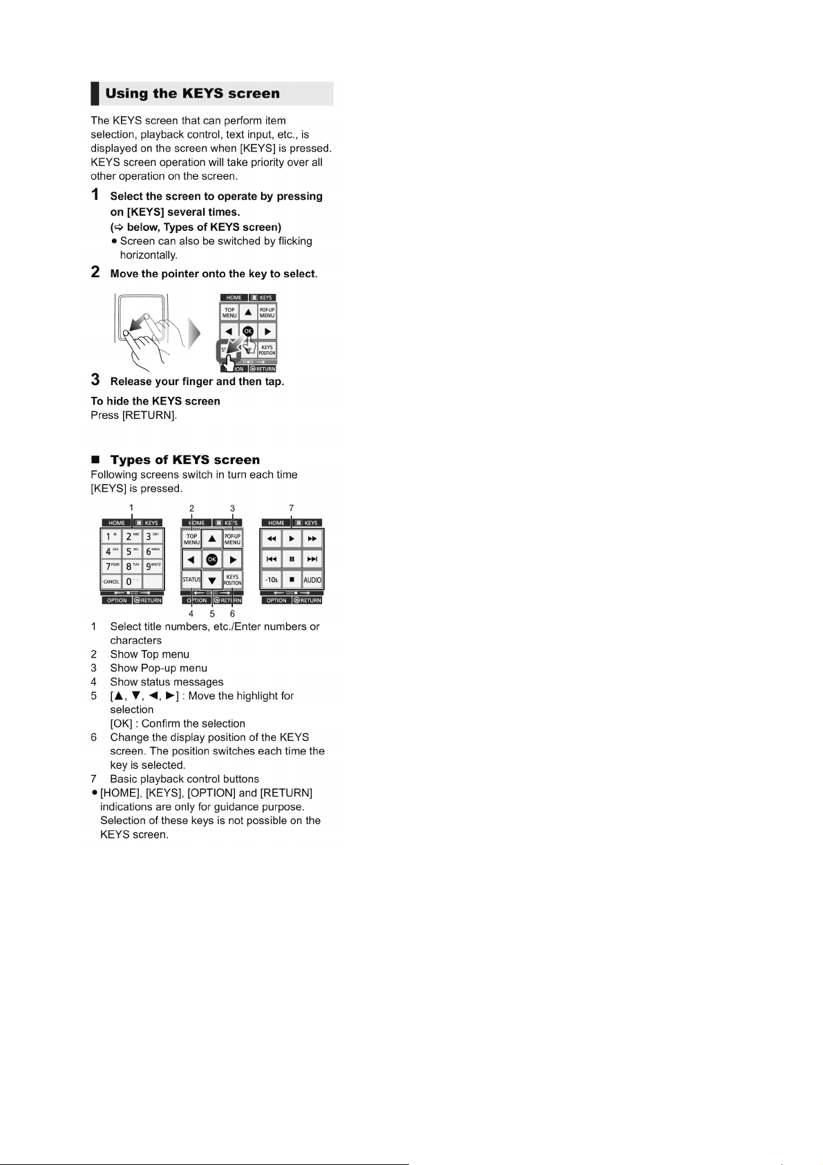
9 Show KEYS screen on the screen
10 Return to previous screen
1
Touch to switch the unit from on to standby
mode or vice versa. In standby mode, the unit
is still consuming a small amount of power.
2Discslot
3 Eject the disc*
4 Remote control signal sensor
One of the two sensors will operate
depending on the installation method of the
main unit.
Distance: Within approx. 7 m
Angle (Against front of the sensor):
Approx. 20G up and down, 30G left and right
5 SD card slot
6 USB port
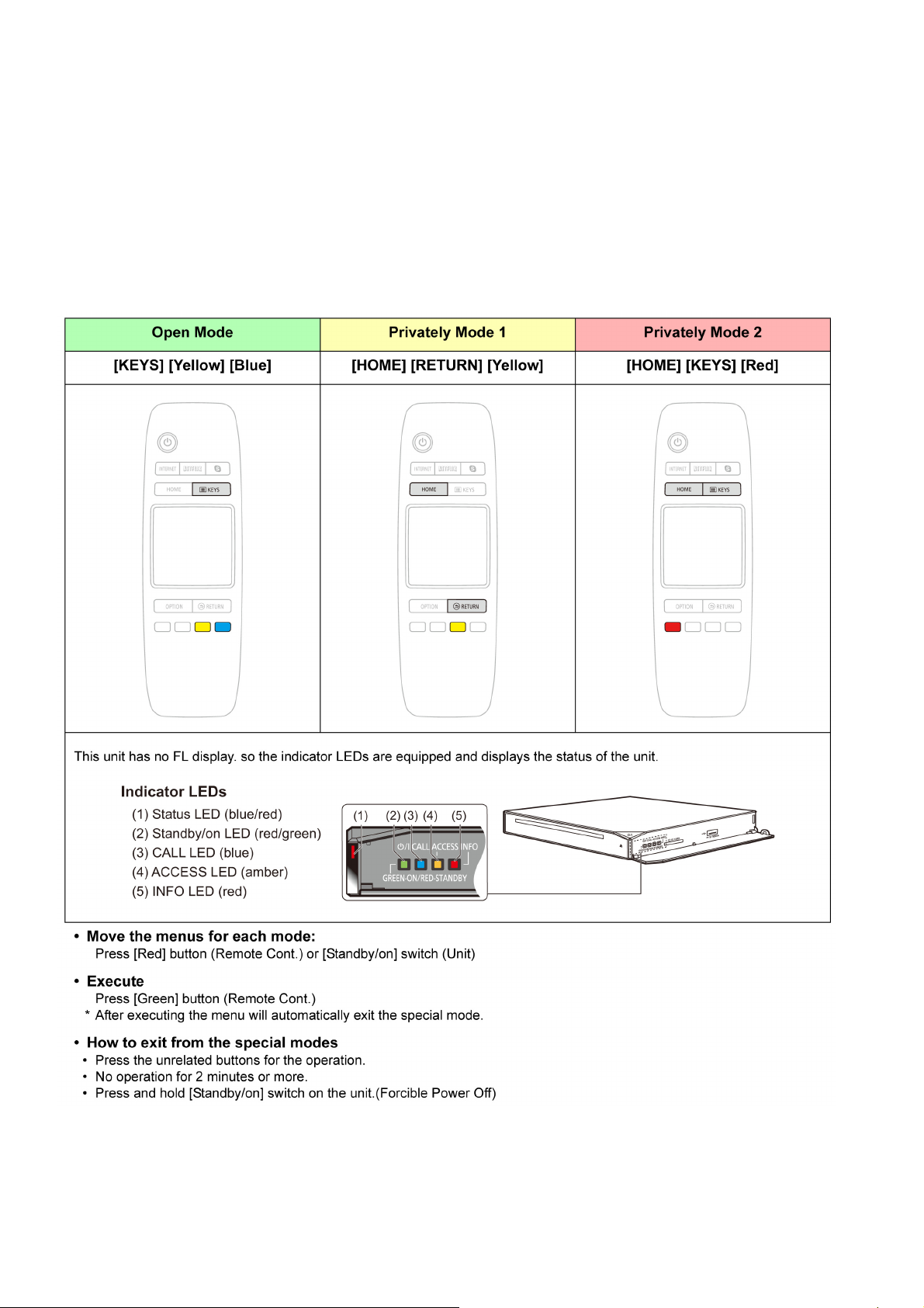
7 Status LED (blue/red)
This will light up in blue when the unit is
turned on.
Blue and red will light up simultaneously
when an error occurs.
This will flash in blue when this unit
receives incoming call etc. of the video
communication.
8 Standby/on LED (red/green)
When the unit is connected to the AC mains
supply, this indicator lights red in standby
mode and lights green when the unit is turned
on. It is also possible to set to turn off when
the unit is in standby mode.
9 CALL LED (blue)
The LED will light up when this unit receives
incoming call etc. of the video
communication.
10 ACCESS LED (amber)
This will flash while accessing the SD card or
USB device.
11 INFO LED (red)
This will light up at the time of error, etc.
* These switches work just by touching the marks. Be
careful not to touch them unintentionally.
The volume of operation sound can be adjusted by “Unit
Operation Volume”.
Standby/on switch* (
/I)
Ɣ
Ɣ
Ɣ
1
INTERNET
2
3
4
HOME
KEYS
5
6
OPTION
RETURN
Indicator LEDs
7891011
7
8
9
10
1
2
3
4
56
14
Pull to flip down
the panel.
Page 15
151617
Page 16
Page 17
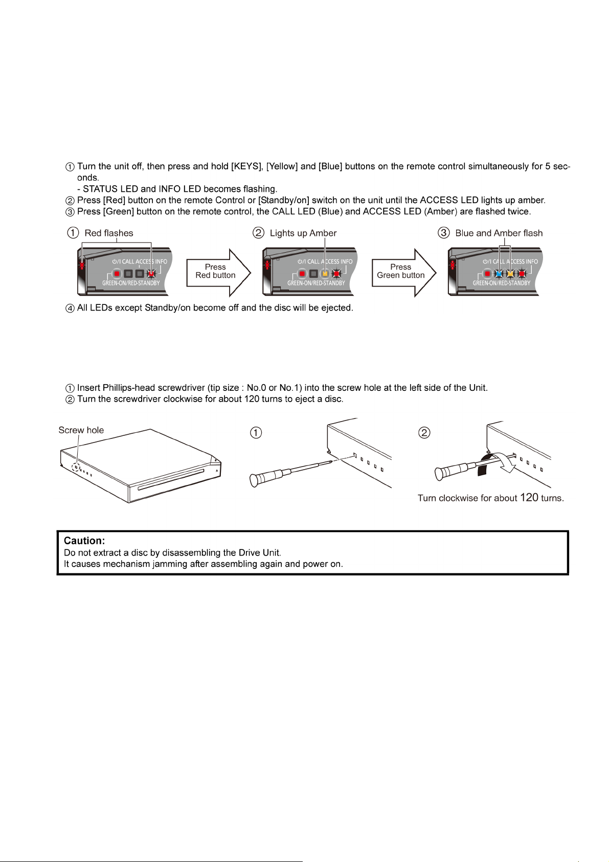
6 Operating Instructions
6.1. Taking out the Disc from Drive Unit when the Disc cannot be ejected by [Eject] switch
6.1.1. Forcible Disc Eject
6.1.1.1. When the power can be turned off.
6.1.1.2. When the power can not be turned off.
Press [Standby/on] switch on the unit for over 4 seconds to turn off the power forcibly, and step 1 to 3 above.
6.1.1.3. When above methods are not effective.
Page 18
7 Multiple Pressing Function
7.1. About the Multiple Pressing of the Unit’s Remote Control
The remote control which included this unit is possible pressing multiple buttons simultaneously (Multiple Pressing function), and
can operate for the customer’s initial settings and the Service Mode, etc.
The Multiple Pressing function is not available for conventional models’ remote control. Use the remote control included this unit.
7.2. How to enter the Special Modes using the Multiple Pressing Function of the Unit’s Remote Control
For pressing the multiple buttons of the remote control, this unit can be entering each of the following special modes.
After entering each mode, and then go to the menu you want to run.
18
Page 19
7.2.1. Open Mode (Remote Cont. Buttons: [KEYS] [Yellow] [Blue])
When pressing the 3 buttons, [KEYS], [Yellow] and [Blue] simultaneously for 5 seconds,
INFO LED becomes flashing Red (Normal speed) and Status LED becomes flashing same timing.
19
Page 20
20
Page 21
7.2.2. Privately Mode 1 (Remote Cont. Buttons: [HOME] [RETURN] [Yellow])
When pressing the 3 buttons, [HOME], [RETURN] and [Yellow] simultaneously for 5 seconds,repeatedly.
21
Page 22
7.2.3. Privately Mode 2 (Remote Cont. Buttons: [HOME] [KEYS] [Red])
When pressing the 3 buttons, [HOME], [KEYS] and [Red] simultaneously for 5 seconds,
INFO LED becomes flashing Red (fast speed) and Status LED becomes flashing same timing.
22
Page 23
23
Page 24
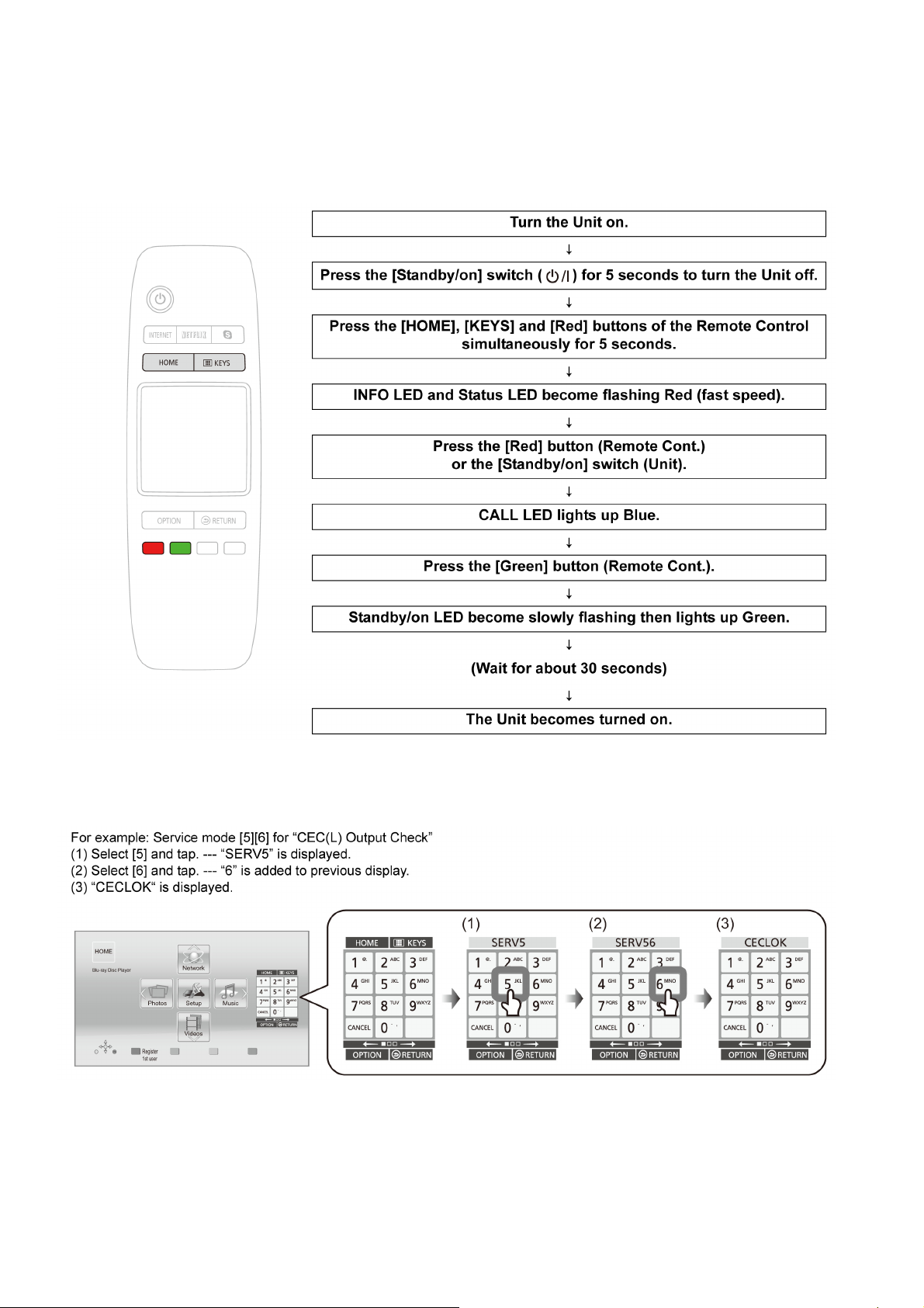
8 Service Mode
8.1. About the Service Mode
Informations necessary for service can be displayed. Connect the display via the HDMI cable before into the service mode.
8.1.1. How to enter the Service Mode
8.1.2. How to operate the Service Mode
Select the Ten Key pad screen by pressing on [KEYS] several time.
While the Ten Key pad screen is displayed, select numeric key and tap for service mode.
8.1.3. How to exit the Service Mode
Press and hold the [Standby/on] switch (remote control or unit).
>>> The Service Mode is terminated and automatically turns the unit off.
24
Page 25
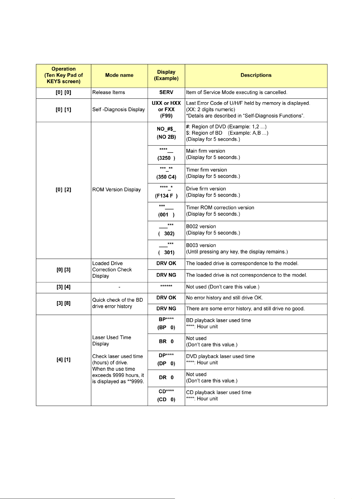
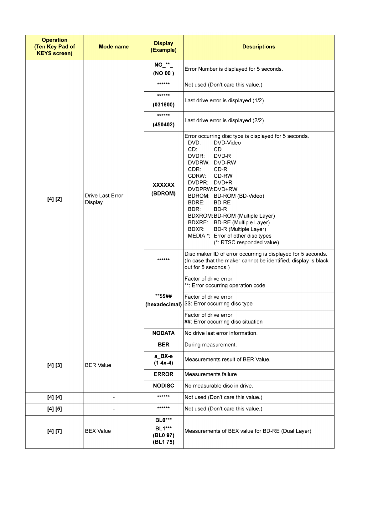
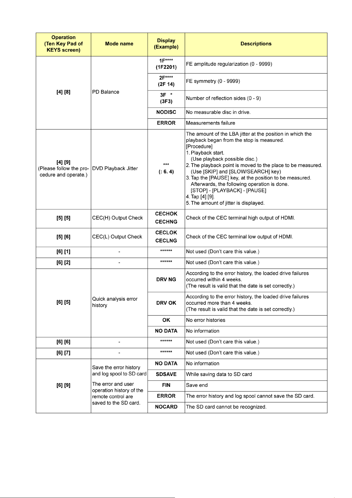
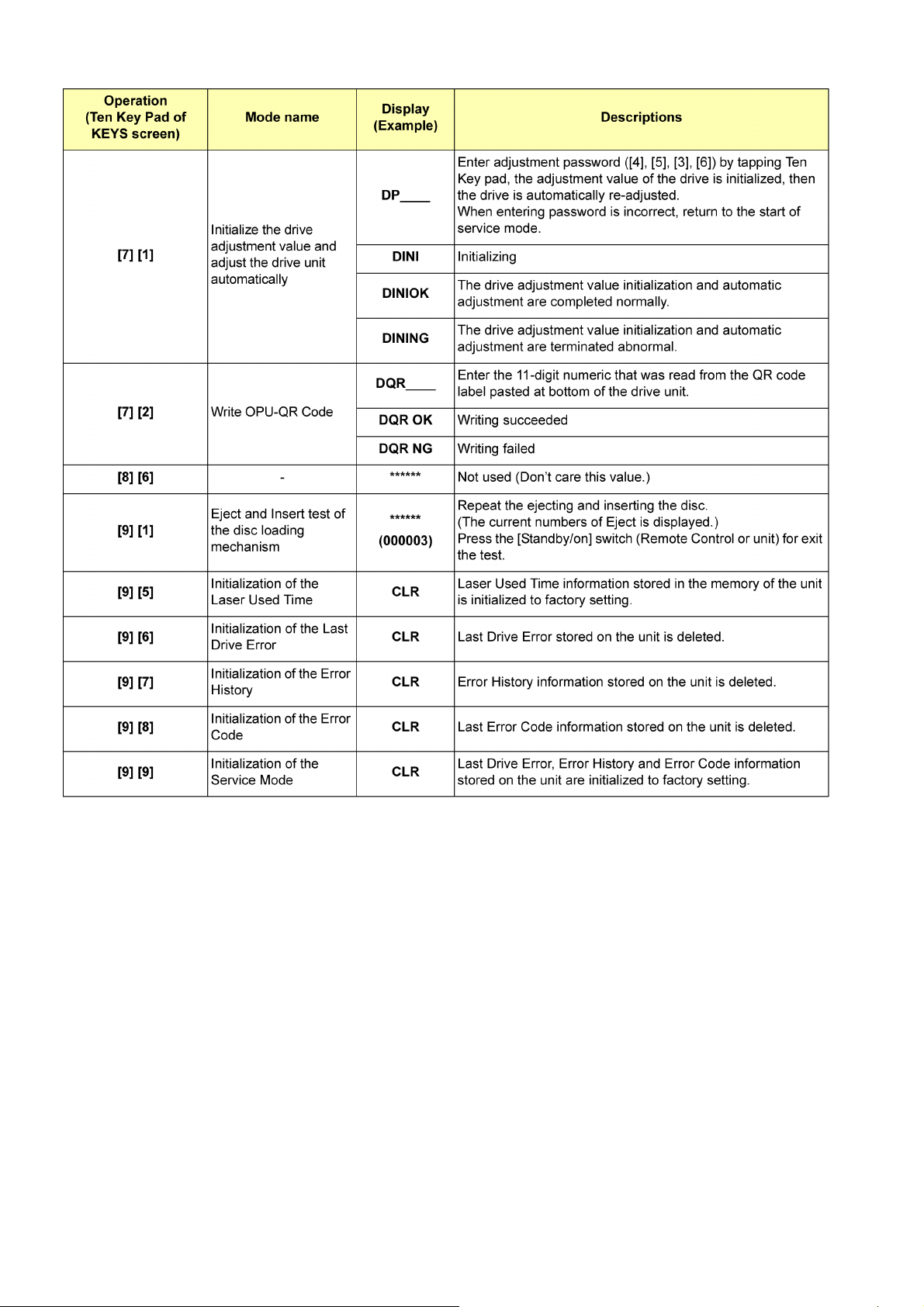
8.2. Service Mode List
The display of information to each command is as follows.
Note:
Do not use it excluding the designated command.
25
Page 26
262728
Page 27
Page 28
Page 29
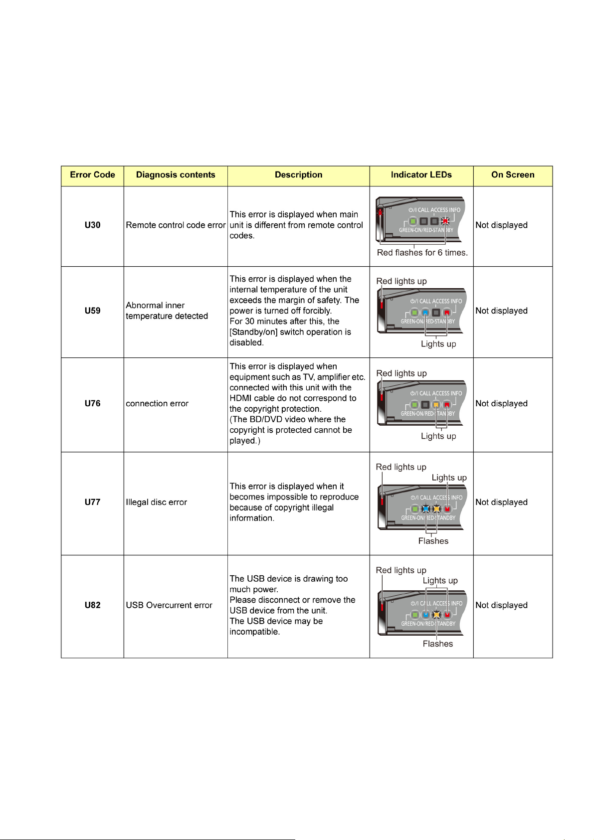
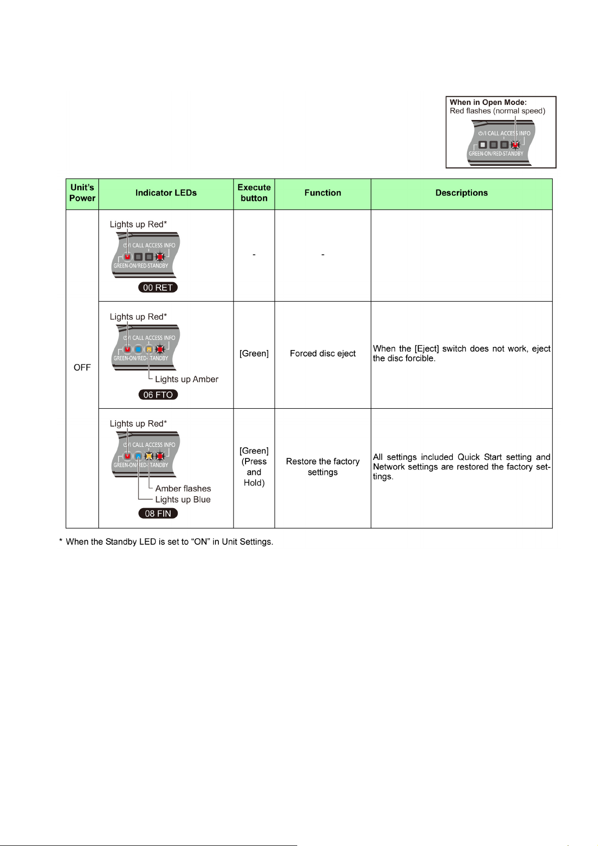
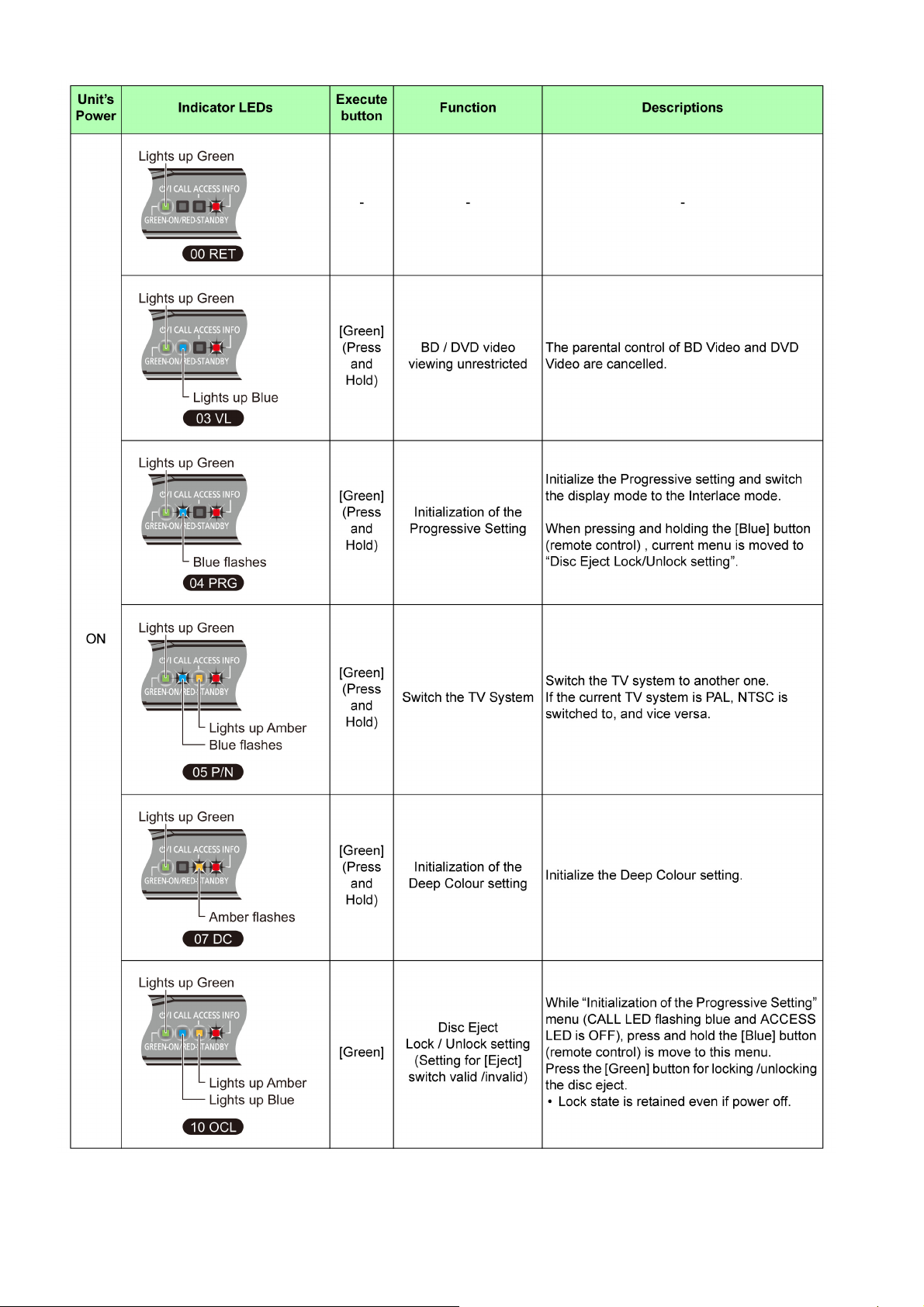
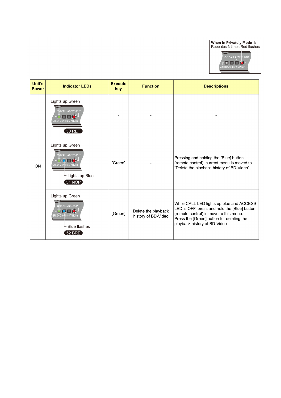
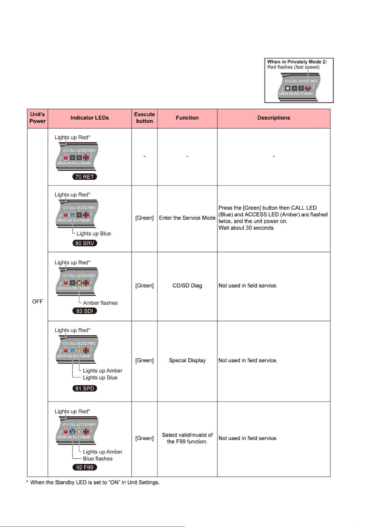
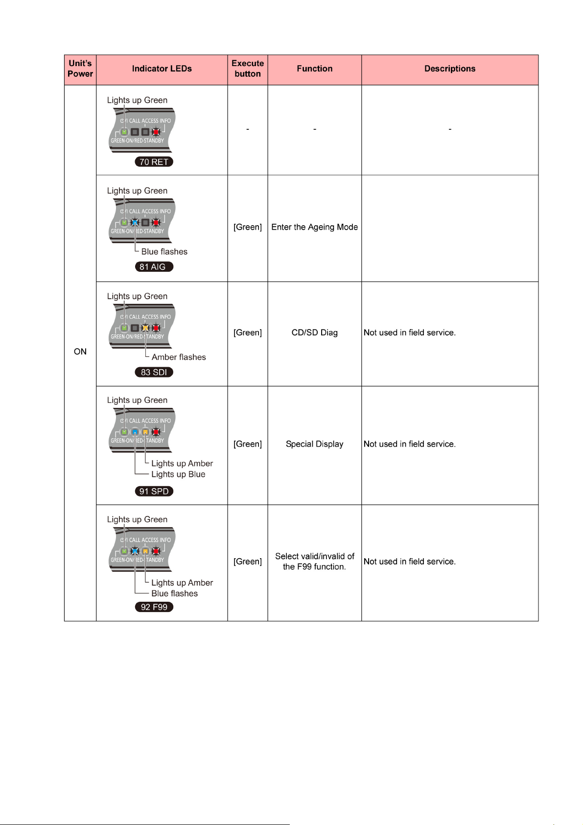
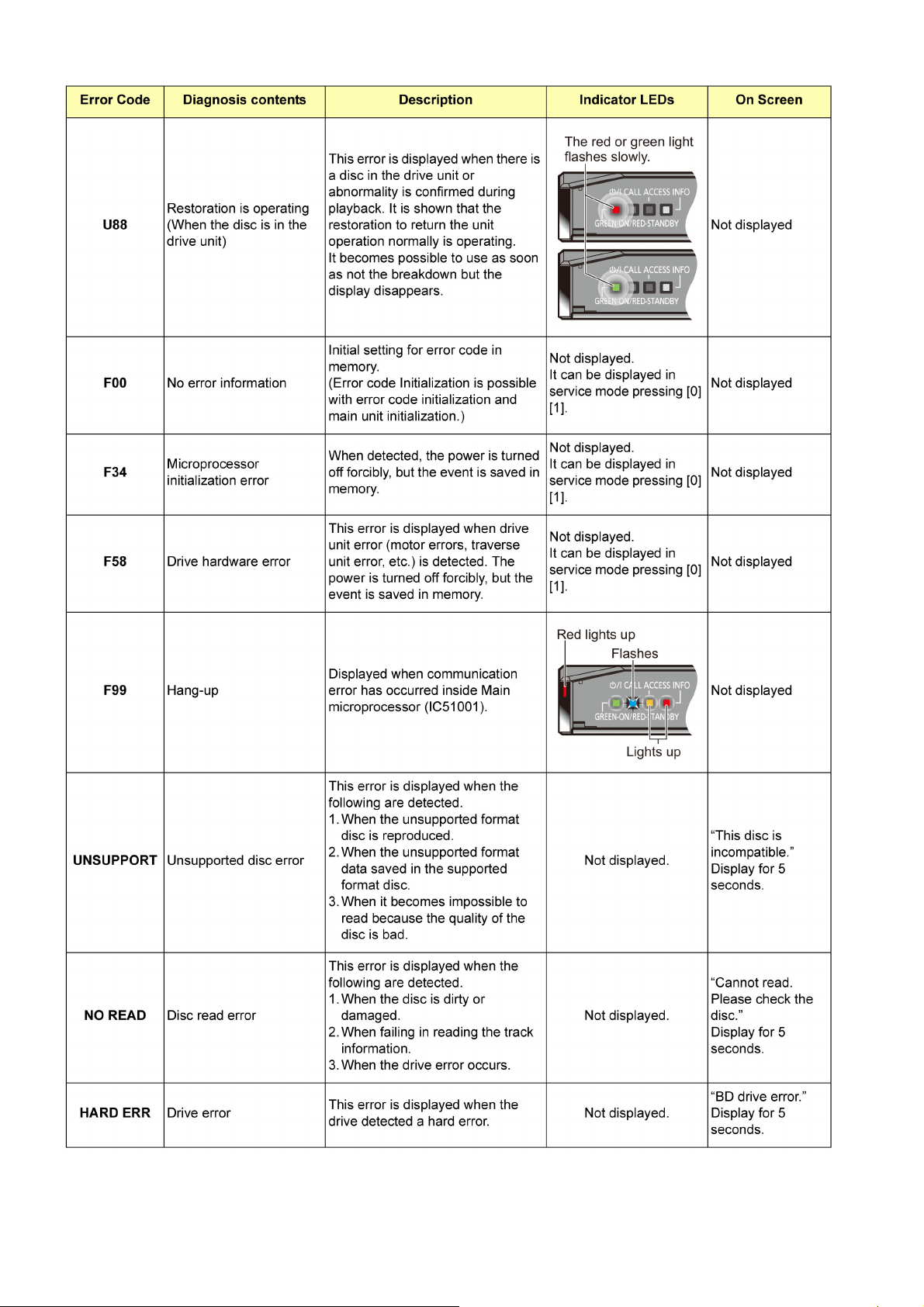
8.3. Self-Diagnostics Functions
8.3.1. Self-Diagnostics Functions
Self-Diagnosis Function provides information for errors to service personnel by Self-Diagnosis Display when any error has
occurred.
U**, H** and F** are stored in memory and held.
You can check last error code by transmitting [0] [1] in Service Mode.
Automatic Display on Indicator LEDs will be cancelled when the power is turned off or AC input is turned off during self-diagnosis
display is ON.
29
Page 30
303132
Page 31

Page 32

9 Service Fixture & Tools
*The above parts are supplied by AVC-CSC-SPC.
Page 33

10 Disassembly and Assembly Instructions
10.1. Unit
10.1.1. Disassembly Flow Chart
The following chart is the procedure for disassembling the casing and inside parts for internal inspection when carrying out the servicing.
To assemble the unit, reverse the steps shown in the chart below.
10.1.2. P.C.B. Positions
33
Page 34

10.1.3. Top Case
1. Remove the 4 screws (A).
2. Open the door unit and remove the screw (B).
3. Unlock the 11 tabs and remove the top case unit.
3. Remove the front panel unit.
10.1.5. Door Unit
1. Open the door unit.
2. Pull out the locking tab of the door unit in direction of the
arrow (1).
3. Remove the door unit in direction of the arrow (2).
10.1.4. Front Panel Unit
1. Remove the FFC(A).
2. Unlock the 3 tabs.
34
Page 35

10.1.6. Bottom Case
1. Spread a little chassis unit and bottom case in the
direction of the arrow (1) and unlock the 2 tabs.
then slide the bottom case a little in the direction of the
arrow (2).
(Sliding the bottom case becomes the 5 locking tabs
unlocked.)
2. Remove the bottom case in direction of arrow (3).
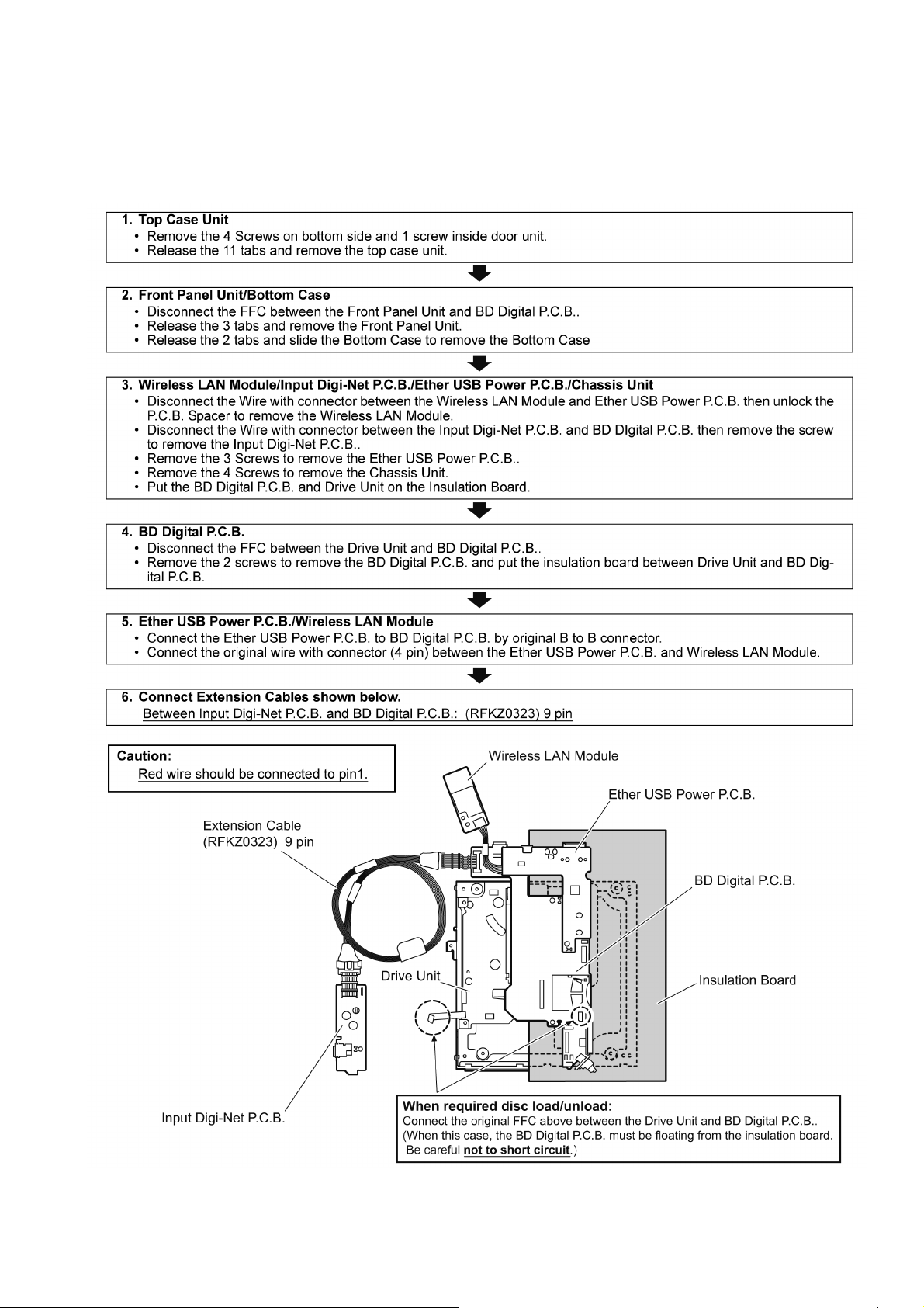
10.1.7. Wireless LAN Module
1. Remove the connector (A).
2. Unlock the P.C.B. spacer and remove the wireless LAN
module.
10.1.8. Input Digi-Net P.C.B.
1. Remove the wire with connector (A).
2. Unscrew the screw (A) to remove the input digi-net
P. C . B . .
35
Page 36

10.1.9. Ether USB Power P.C.B.
1. Remove the screw (A) and 2 screws (B).
2. Remove the ether USB power P.C.B. in direction of arrow.
10.1.10. LED Buzzer P.C.B. and IR LED P. C .B .
1. Remove the LED buzzer P.C.B. and IR LED P.C.B. in
direction of arrow.
10.1.11. Chassis Unit
1. Remove the 4 screws (A).
2. Remove the chassis unit in direction of arrow.
36
Page 37

10.1.12. BD Digital P.C.B. and Drive Unit
1. Pull out the Diffused Sheet.
2. Remove the FFC (A), and isolate it with an ESD prevention bag (RPFC0114).
3. Remove the Connector (A), FFC (B) and FFC (C).
4. Remove the 2 screws (A).
5. Remove the FFC (D) then remove the drive unit from the
BD digital P.C.B..
6. Unscrew the 2 screws (B) to remove the drive angle.
37
Page 38

10.2. Drive Unit
10.2.1. Bezel and Tray Door
1. Unlock 7 tabs (A) and 2 tabs (B) to remove the Bezel and
Tray Door.
10.2.2. Top Cover Unit
1. Unscrew the 2 screws (A) and remove the Top Cover
Unit.
38
Page 39

10.2.3. Bottom Cover
1. Unscrew the 4 screws (A) and remove the Bottom Cover.
3. Unscrew the 2 screws (A) and unlock the locking tab (A)
to remove the FPC bracket.
4. Remove the Radiator sheet with FPC sheet.
10.2.4. OPU and Nut Piece Unit
1. Turn over the drive unit.
2. Slide the OPU Sheet and OPU FPC to release from slit of
the FPC bracket.
39
Page 40
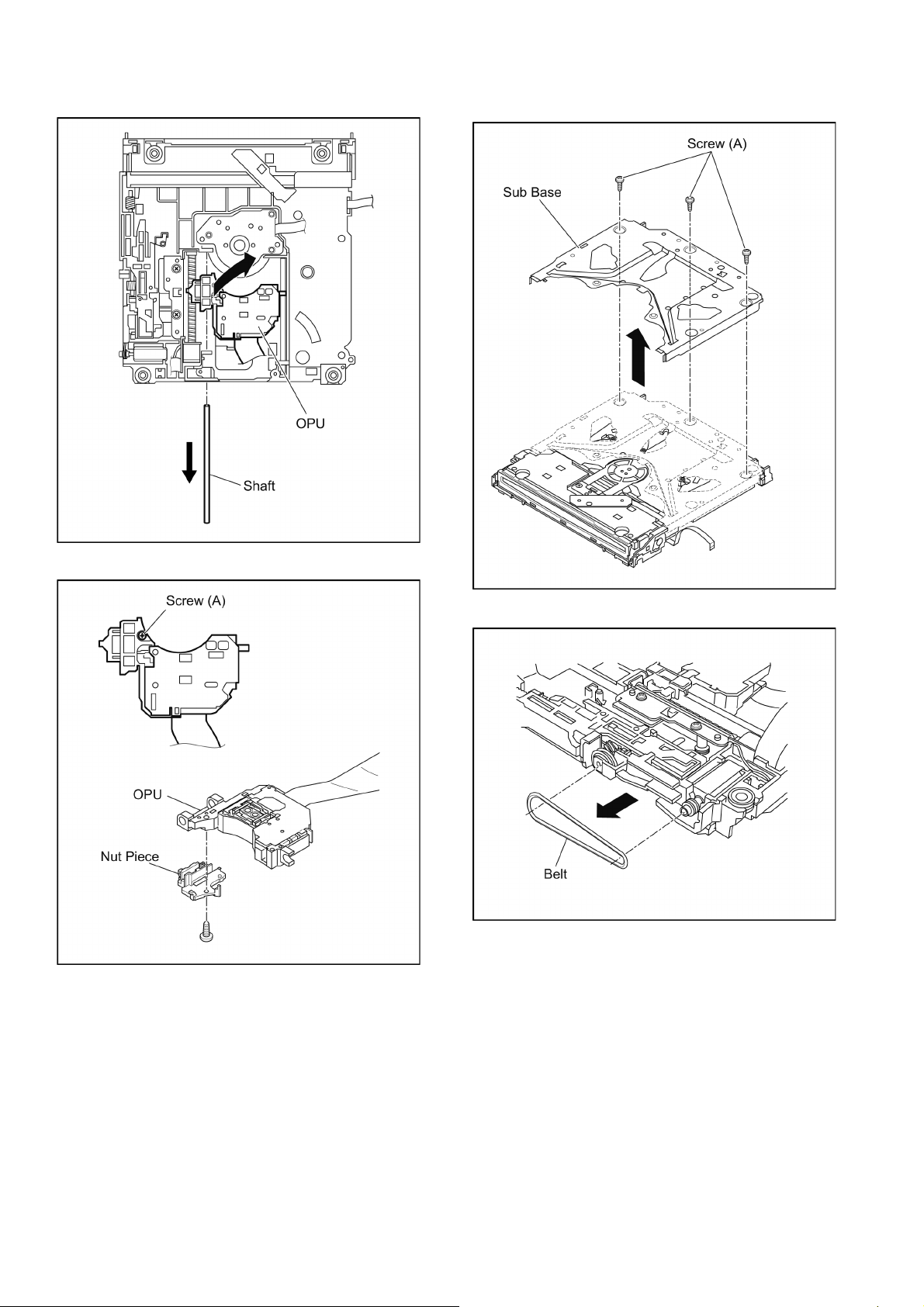
5. Remove the shaft then remove the OPU shifted slightly
diagonally.
10.2.5. Belt
1. Unscrew the 3 screws (A) to remove the the Sub Base.
6. Unscrew the screw (A) and remove the Nut Piece.
2. Remove the belt.
40
Page 41
11 Measurements and Adjustments
11.1. Service Positions
For description of the disassembling procedure, see the “10 Disassembly and Assembly Instructions”.
11.1.1. Checking and repairing
41
Page 42

11.2. Adjustment of Drive Unit/BD Digital P.C.B.
11.2.1. Checking out symptoms and repair of Drive Unit/BD Digital P.C.B.
42
Page 43

11.2.1.1. Analysis Procedures
1. Confirmation the pointed symptom - 1
After replacing the BD Digital P.C.B. with normal one, carry out the drive automatic adjustment using the Service Mode [7][2]
and [7][1], confirm the pointed symptom occurs again.
• When the pointed symptom not occurs:
Original BD Digital P.C.B. is defected, go to Step 2.
• When the pointed symptom occurs:
The drive unit is defective, go to Step 3.
2. Replacing BD Digital P.C.B. with the original one, carry out the failure analysis and repair, go to Step 4.
3. Replacing BD Digital P.C.B. with the original one, carry out the drive automatic adjustment using the Service Mode [7][2] and
[7][1].
• When the pick-up unit is defected, replace the pick-up unit with normal one.
• When exterior parts or mechanism are defected, replace the defective parts.
4. Confirmation the pointed symptom - 2
Carry out the drive automatic adjustment using the Service Mode [7][2] and [7][1], recheck the pointed symptom and failure
not occurs.
• When the pointed symptom occurs again, go to Step 1.
11.2.2. In the Case of Necessity the Adjustment
1. When the OPU ass’y is replaced.
2. When the Drive Unit is replaced.
3. When the BD Digital P.C.B. is replaced.
43
Page 44

11.2.3. Adjustment Procedure
44
Page 45

11.3. Caution for Replacing Parts
After replacing the BD Digital P.C.B., [TEST] is displayed, so, once power off again to on.
11.3.1. Caution after replacing parts
After replacing the Drive Unit/BD Digital P.C.B., must be update Firmware.
11.3.2. Standard Inspect Specifications after Repairs
After making repairs, we recommend performing the following inspection, to check normal operation.
45
Page 46

12 Block Diagram
OVERALL BLOCK DIAGRAM
DMP-BBT01EB/EG OVERALL BLOCK DIAGRAM
TRAVERSE MECHANISM UNIT
OPTICAL
PICK-UP
UNIT
IC51001
SERVO CONTROLLER/
OPTICAL DISC CONTROLLER/
AV DECODER/
SYSTEM CONTROLLER
LED
BUZZER
LASER DIODE
FOCUS COIL
BEAM EXPANDER
TRACKING COIL
STEPPING
MOTOR
SPINDLE
MOTOR
LOADING
MOTOR
SD CARD
IC59020
IC51301
NAND FLASH
ROM/2Gbit
PHYSICAL LAYER
TRANSCEIVER
JK59001
ETHERNET
PORT
IC52001
SDRAM/2Gbit
SDRAM/2Gbit
IC52002
MPX/DE-MPX
IC57101
REMOTE
SENSOR
REMOTE
SENSOR
X51001
(27MHz)
IC55004
DISC
MOTOR
DRIVER
P59601
TOP SENSOR
IC57501
USB PORT
(FRONT)
P59301
HIGH SIDE SWITCH
IC59303
HIGH SIDE SWITCH
IC59304
IC59305
USB HUB
CONTROLLER
WIRELESS
LAN
MODULE
IC53002
DIGITAL
AUDIO OUT
(OPTICAL)
(JK56301)
HDMI
JACK
12.1. Overall Block Diagram
46
Page 47

12.2. Input Digi-Net P.C.B. Regulator Circuit Block Diagram
DMP-BBT01EB/EG INPUT DIGI-NET P.C.B. REGULATOR CIRCUIT BLOCK DIAGRAM
P58002
P58001
P58002 P58001
1,2
3,4
P58002 P58001
9
PW X SW5.9V
P58002
P58001
5
PW ST D3.3V
P58002
P58001
8
IR SEL
SW58001
PW X SW12.2V
P STANDBY H
From/To BD DIGITAL P.C.B.
INPUT DIGI-NET P.C.B. REGULATOR CIRCUIT BLOCK DIAGRAM
IC58003
(REGULATOR +3.3V)
13
Vin
14
Vcc
Vfb
1
7
2
Vo
EN
12
Vbst
10
SW1
SW2
11
CKH1
CKH2
CL58003
CKZ1
CKZ3
CKZ5
CKZ9
CKZ8
CL58005
QR58002
123
4
6
5
Q58002
JK58001
1
3
2
DC
JACK
IP58001
IP58002
Q58001
IC58303
(REGULATOR +5.9V)
8
Vin
Vfb
2
EN
7
Vbst
SW
6
1
47
Page 48

12.3. BD Digital P.C.B. Regulator Circuit Block Diagram
DMP-BBT01EB/EG BD DIGITAL P.C.B. REGULATOR CIRCUIT BLOCK DIAGRAM
BD DIGITAL P.C.B. REGULATOR CIRCUIT BLOCK DIAGRAM
LDD VCC
(P55006-20)
TL55004
IC58302
(REGULATOR +5V)
2
VIN
5
4
1
VO
CN
CONT
DR P ON H
(From IC51001-D14)
QR58001
IC57006
(REGULATOR +3.3V)
4
1
5
VOUT
ON
VIN
CL57003
IC56302
(REGULATOR +5V)
5
VIN
4
1
VOUT
ON
CL57119
HDMI P ON H
(From IC51001-A13)
IC55300
(REGULATOR +5V)
1
Vout
PW HDMI5V
( To JK56301-18)
PW ST D3.3V
CKS18
CL57034
IC55006
(REGULATOR +5V)
2
VC
3
1VOVIN
CL55294 CL55295
CL55003
CL55002
CL55296
CL55297
CL55001
CL55030
IP55005
D5V
(To IC55004-29,37,40)
LDD BVCC
(P55006-15)
PDIC VCC
(To P55006-27)
PW DR12V
(To IC55004-45,54.55)
8
Vin
PW X SW3.3V
IC57003
(REGULATOR +1.2V)
5
1
3
VOUT
VDD
CE
CL57011
VDD12STM
( To IC51001-F8)
IC58004
(REGULATOR +1.5V)
13
Vin
14
Vcc
Vfb
1
7
2
Vo
EN
12
Vbst
10
SW1
SW2
11
From/To INPUT DIGI-NET P.C.B.
P58001P58002
1,2
P58001P58002
3,4
PW X SW12.2V
PW X SW5.9V
IC58005
(REGULATOR +1.1V)
13
Vin
14
Vcc
Vfb
1
7
2
Vo
EN
12
Vbst
10
SW1
SW2
11
CL58001
PW PK D1.5V
CL58002
PW PK D1.1V
CL58004
CL58006
PW USB 5.1V
IC58203
(REGULATOR +5.1V)
8
Vin
Vfb
2
EN
7
Vbst
SW
6
1
CL57203
P STANDBY H
(From IC51001-B15)
P58001
P58002
9
P STANDBY H
123
4
6
5
Q58006
CKW1
P58001P58002
5
PW ST D3.3V
CKW5
CKW9
CKW3
IP55004
5 CONT
VDD33STM
( To IC51001-F7)
48
Page 49

12.4. Digital Video/Audio Circuit Block Diagram
DMP-BBT01EB/EG DIGITAL VIDEO/AUDIO CIRCUIT BLOCK DIAGRAM
: VIDEO PB SIGNAL
:
AUDIO PB SIGNAL
DIGITAL VIDEO/AUDIO CIRCUIT BLOCK DIAGRAM
IC53002
(OPTICAL FIBER
TRANSMITTER)
IC51001
(PEAKS-PRO4)
AO2IEC
K4
1
2
G OPTIEC
VIN
VCC
DRIVE
IC
PW ST D3.3V
CK54001
CK54002
CK51010
4 8
73
1
3
19
16
CL56301CL57118
CKS15
CKS16
CKS13
CKS19
CKS18
JK56301
(HDMI JACK)
D2+
D2-
2 6
51
4
6
D1+
D1-
L56301
L56302
4 8
73
7
9
D0+
D0-
2 6
51
10
12
CLK+
CLK-
HDMISDA
HOTPLG
15
HDMISCL
HTTX2P
HTTX2M
HTTX1P
HTTX1M
HTTX0P
HTTX0M
HTTXCP
HTTXCM
HTSCL
HTSDA
HTHPD
A5
B5
A4
B4
A3
B3
A2
B2
E7
E6
D7
SMPIO07
HDMI CEC
B12
13
CEC
18
+5V
PW HDMI5V
(From IC56302-4)
Q56301
PW X SW5.9V
49
Page 50

12.5. Digital (Front End Section) Circuit Block Diagram
DMP-BBT01EB/EG DIGITAL (FRONT END SECTION) CIRCUIT BLOCK DIAGRAM
DIGITAL(FRONT END SECTION) CIRCUIT BLOCK DIAGRAM
IC51001
(PEAKS-PR04)
CL55040
CL55055
CL55053 CL55054
CL55099 CL55098
CL55144 CL55143
CL55146 CL55145
CL55093 CL55092
CL55091
CL55411
CL55410
CL55097
CL55096
CL55095
CL55094
CL55090
CL55052
OPTICAL PICK-UP/TRAVERSE
SPINDLE
MOTOR
STEPPING
MOTOR
FO/TR
ACTUATOR
LASER DIODE
DRIVE(LDD)
LASER
DETECTOR
LASER
DETECTOR
LASER
DETECTOR
DVD
CD
BD
P55006
P55401
P55011
BD/DVD
RF SIGNAL
FOCUS/TRACKING ACTUATOR
SPINDLE MOTOR DRIVE
STEPPING MOTOR DRIVE
DVD FOCUS AND TRACKING SIGNAL
LD CONTROL SIGNAL
BD FOCUS AND TRACKING SIGNAL
CD MAIN AND SUB SIGNAL
BEAM EXPANDER
B19
PWM1A
C18
PWM0B
B17
PWM3B
C19
PWM2A
PWM3A
A17
P12
L23
P13
L22
FG
B20
PWM4
C17
RF SIGNALMOTOR DRIVE SIGNALTRACKING ERROR SIGNALFOCUS ERROR SIGNAL
IN1
Logic
IN47
VREF
STBY
IN58
DAT
CK
EN
FG
INS6
Pre-Drive
V
DD
FO1
G FO2+
G FO2-
G FO1+
G FO1-
G TR+
G TR-
G SA+
G SA-
G SB+
G SB-
G TRVA+
G TRVA-
G TRVB+
G TRVB-
G U
G V
G W
RO1
Logic
Pre-Drive
Pre-Drive
Pre-Drive
Pre-Drive
FO7
RO7
FO8
RO8
FO4
RO4
FO5
RO5
Logic
Upper
Pre-Drive
Upper
Pre-Drive
OSC
Serial
Distribution
Circuit
Stand-by
(ALL)
IC55004
(MOTOR/PWM/DRIVER)
IN2
Logic
Pre-Drive
FO2
RO2
IN3
Logic
Pre-Drive
FO3
RO3
V
DD
V
PUMP
DMOS
3-phase
bridge
Generate
FG
A1
COM
A2
A3
RCS1
ABS
Logic
Pre-Drive
V
DD
DMOS
H/B
FO6
RO6
DMOS
H/B
DMOS
H/B
DMOS
H/B
DMOS
H/B
DMOS
H/B
DMOS
H/B
DMOS
H/B
G LDM-
G LDM+
LOADING
MOTOR
PWM1A
A19
PWM0A
P14
M23
PWM0A
PWM2A
VHALFIN
PWM3A
PWM0B
PWM3B
G SDIO D
G SCLK D
G SEN D
FG
PWM4
P55401
P55401
7
8
39
38
53
52
51
56
47
46
43
41
36
35
34
33
32
31
25
24
22
20
18
7
10
6
9
12
13
11
14
8
27
26
48
RCS2
CS
GND
49
1
16
E23
VHALFOUT
RL55045
RL55152 RL55153
RL55154
RL55039
RL55041
RL55044
RL55043
RL55079
RL55078
B22
PAD0
D22
PAD1
K23
P10
P12
P13
L23
L22
P14
M23
G26
RFA
G25
RFB
F25
AIN
E26
BIN
E25
CIN
D26
DIN
D25
EIN
C26
FIN
B26
GIN
C25
HIN
50
Page 51

12.6. Digital (Back End Section [1]) Circuit Block Diagram
IC51001
(PEAKS-PRO4)
DMP-BBT01EB/EG DIGITAL(BACK END SECTION[1]) CIRCUIT BLOCK DIAGRAM
DIGITAL(BACK END SECTION [1]) CIRCUIT BLOCK DIAGRAM
CK27XO
CK27XI
X51001
(27MHz)
B10
A10
BD DIGITAL P.C.B.
IC59020
(ETHERNET CONTROLLER)
JK59001
(ETHERNET JACK)
11
10
4
5
TX+
TX-
RX+
RX-
CK59631
10M
100M
WOL
5B 4B
Decoder
(LPI Detection)
TXC10
TXD
TXC25M
RXD
RXC25M
TXD10
RXC10
RXD10
10/100
Half /Full
Switch
Logic
10/100M Auto Negotiation
Control Logic
(EEE Capability Exchange)
Manchester Coded
Waveform
Data Recovery
Receive Low Pass Filter
10M Output Waveform
Shaping
(Amplitude Reduction)
TXO+
MDI+[0]
MDI-[0]
MDI+[1]
MDI-[1]
TXO-
RXIN+
RXIN-
CK25O
PLL
MASTER
CKXTAL1
MII RXD3
MII RXD2
MII RXD1
MII RXD0
MII TXD0
MII TXD1
MII TXD2
MII TXD3
RXD3
RXD2
RXD1
RXD0
TXD0
TXD1
TXD2
TXD3
MII RXCLK
RXC
MII RXER
RXER
MII RXDV
RXDV
MDIO INTL
INTB
PHYRSTL
PHYRSTB
MII TXEN
TXEN
MII TXCLK
TXC
MDC
MDC
MDIO
MDIO
31
PMEB
10
1
2
4
5
22
27
23
24
25
26
13
19
39
18
17
16
14
32
29
42
30
Y4
Y2
Y3
W6
Y1
W4
AB1
AA2
AA3
AA4
AC3
AC2
AC1
AE1
AB3
AD2
AD1
AB2
RL59007
RL59004
RL59002
RL59008
MII CRS
CRS
36
W5
RL59011
MII COL
COL
38
Y5
RL59010
RL59003
CL59003
CL59001
IC59305
(USB HUB CONTROLLER)
CKJ59301
CKA59629
CKA59608
CKA59609CK59635
CKA59630
CK59602
CK59601
CK59634
CKJ59302
CKJ59303
X59301
(30MHz)
SD0CMD
SD0CLK
SD0CD
SD0WP
SD0DAT0
SD0DAT1
SD0DAT2
SD0DAT3
7
8
9
1
2
5
10
12
DAT0
DAT1
DAT2
DAT3
CMD
CLK
CD
WP
3.3V
11
P59601
(SD CARD SLOT)
PW USB 5.1V
PW USB 5.1V
P59602P59603
301
P59602P59603
292
P59602P59603
922
P59602P59603
823
P59602P59603
328
P59602P59603
229
P59602P59603
625
P59602P59603
526
2 3
41
T59301
3
1
2
DN
DP
VBUS
IC59303
(HIGH SIDE SWITCH)
VIN
VOUT
/EN
/OC
3
4
1
5
FRONT-SIDE
(H-type)
USBDN1
AF22
USBDP1
AE22
4B
3.3V
4A
PW ST D3.3V
P59303
4
P59303
2
P59303
3
25
26
45
46
DM1
DP2
PPB1
CSB1
CKJ59013
IC59304
(HIGH SIDE SWITCH)
VIN
VOUT
/EN
/OC
3
4
1
5
43
44
PPB2
CSB2
DP1
21
22
1
10
11
DMU
DPU
VDD33
VDD33
VDD33
VBUSM
VDD25OUT
12
VDD25
19
AVDD
24
VDD25
33
VDD25
X1
X2
DM2
CK59011
CK59012
2 3
41
T59302
DP
DN
1 5
62
L59601
3 7
84
29
28
17
AVDD
9
20
30
47
VDD33REG
48
PW ST D3.3V
WIRELESS
LAN MODULE
CKJ59610
CKJ59609
CKJ59606
CKJ59603
CKJ59602
CKJ59601
CKJ59608
CKJ59607
CKJ59605
W25
V23
V25
V24
W24
W26
V22
W23
ETHER USB POWER P.C.B.
PW X SW12.2V
Q57502
Q57501
QR57501
+
BZ51091
BUZZER
SMPIO14
SMPIO16
E13
C12
Data
Alignment
Scrambler
Descrambler
Serial to
Parallel
Parallel to Serial
Supports
EEE Quiet
3 Level
Driver
TD+
Adaptive
Equalizer
ck Slave
3Level
Comparator
MLT-3
to NRZI
PLL
data
4B 5B
Encoder
(LPI Generation)
Variable Current
Link Pulse
RL57002
RL57004
P59301
(USB JACK)
CK59003
CK59004
CKA59602CK59629
CK59628
CK59626
CK59625
CKA59603
CK59005
CKA59605
CK59006
CKA59606
CK59633
CK59605
CK59632
CL59002
51
Page 52

12.7. Digital (Back End Section [2]) Circuit Block Diagram
IC52001
(DDR3 SDRAM/2Gbit)
44
29
IC51301
(NAND FLASH ROM/2Gbit)
DATA
DATA
MMDQ14
MMDQ9
MMA13
MMA0
ED0
ED7
IO0
IO7
MMDQ2
MMDQ3
A3
D7
H7
E3
AC7
AB9
AD4
AC5
AD14
AF10
A13
A0
DQU7
DQU0
DQL7
DQL0
M3
N8
BA2
BA1
M2
BA0
AB13
AE13
MMBA2
MMBA1
AD9
MMBA0
T3
N3
AF25
AC25
ADDRESS
BANK BANK
M3
N8
BA2
BA1
M2
BA0
BANK
ADDRESS
IC51001
(PEAKS-PRO4)
DMP-BBT01EB/EG DIGITAL(BACK END SECTION[2]) CIRCUIT BLOCK DIAGRAM
DIGITAL(BACK END SECTION [2]) CIRCUIT BLOCK DIAGRAM
PW ST D3.3V
12
VCC
37
VCCQ
DATA
DATA
IC52002
(DDR3 SDRAM/2Gbit)
A3
D7
H7
E3
AA16
AB15
AD20
AC18
A13
A0
DQU7
DQU0
DQL7
DQL0
T3
N3
ADDRESS
D
ATA
DATA
MMDQ25
MMDQ31
MMDQ23
MMDQ18
P58001 P58002
1,2
PW X SW3.3V
1
3
REMOCON
IR51921
REMOTE
SENSOR
BD DIGITAL P.C.B.
CK27XO
CK27XI
X51001
(27MHz)
B10
A10
XRST STM
F15
IC57002
(RESET)
1 2
OUT VDD
CL57001
SMPIO05
A14
IC57005
(RESET)
SMPIO22
A11
1 2
OUT VDD
P58001 P58002
3,4
CL57014
CL57031
CL57032
CL57033
CL57103
CL57122
CKD1
INPUT DIGI-NET P.C.B.
TOUCH SW P.C.B.
LED BUZZER P.C.B.
IR LED P.C.B.
P51901P51701
5
REMOCON
PW X SW3.3V
1
3
REMOCON
IR57101
REMOTE
SENSOR
IC57101
(MPX/DE-MPX)
CH0
1
CKJ2
PW X SW12.2V
P58001 P58002
8
IR SEL
PW X SW5.9V
P57501 FT701
1
P57501 FT701
3
D51902
D51901
VDD
1
IC57501
(TOP SENSOR)
ALERT
17
SM CLK
8
SM DATA
6
CS1
CS2
RL701
CS1
CS2
CS1
RL702
CS2
P-ON
D51904
SKYPE
D51903
ACCESS
D51906
INFO
P-OFF
24
CKD3
23
P51701 P51901
8
LED2
CKB8 CKM8
CKM7
CKM5
P51702 P51921
2
CKC2
10
P51701 P51901
7
LED1
CKB7
CKB5
CKB3
CKB2
9
SMPIO17
SMPIO20
D12
E12
PW X SW3.3V
PW X SW5.9V
LED POWER1
INFO LED
P51901P51701
3
CKM3
SKYPE LED
P51901P51701
2
CKM2
USB LED
LED POWER2
D51922
INFO
P51702 P51921
6
CKC6
CKJ6
PW X SW5.9V
INFO LED
QR51902
QR51903
QR51901
QR57502
P51921P51702
5
D51921
SD
CKJ5
CKC5
SD LED
QR51921
SMPIO13
D13
SMPIO21
F12
SMPIO30
C10
D8
SMPIOA2
RL57114
RL57021
RL51107
7
CH1
6
A
VCC
CMMON
5
INH
2
PW X SW3.3V
8
SMPIO23
B11
52
Page 53

13 Wiring Connection Diagram
INTERCONNECTION DIAGRAM
DMP-BBT01EB/EG INTERCONNECTION DIAGRAM
P51701
5R9V 1
USB_LED 2
SKYPE_LED 3
NC 4
INFO_LED 5
LED_PW_CRL 6
LED_POWER1 7
LED_POWER2 8
GND 9
GND 10
P51702
13R3V
2 REMOCON
3GND
45R9V
5SD_LED
6 INFO2_LED
7GND
8GND
9GND
10 GN D
P59603
30 DGND
29 TX+
28 TX27 DGND
26 RX+
25 RX24 DGND
23 BUZZER_P
22 BUZZER_M
21 DGN D
20 DGND
19 PW_ST_ D3R3V
18 PW_ST_ D3 R3V
17 P W_ST_ D3R3 V
16 PW_ ST_D3R3V
15 PW_X_S12R2 V
14 PW_ X_S12 R2 V
13 PW_ X _S12 R2V
12 PW_ X _S12 R2V
11 DGND
10 DGND
9DGND
8DGND
7DGND
6P_STANBY_H
5DGND
4USBEN1
3DGND
2USBDN1
1USBDP1
JK58001
1+12V
2GND
P58002
PW_X_SW12R2V 1
PW_X_SW12R2V 2
PW_X_SW5R9V3
PW_X_SW5R9V 4
PW_ST_D3R3V 5
GND 6
GND 7
IR_SEL 8
P_ STANB Y_H 9
P51921
3R3V 1
REMOCON 2
GND 3
5R9V 4
SD_LED 5
INFO_LED 6
GND 7
GND 8
GND 9
GND 10
INPUT DIGI-NET P.C.B.
IR LED P.C.B.
BD DIGITAL P.C.B.
WIRELESS LAN MODULE
AC ADAPTOR
TOUCH SW P.C.B.
LED BUZZER P.C.B.
ETHER USB POWER P.C.B.
P55006
OL-ACT FOC2+ 1
OL-ACT FOC2- 2
OL-ACT TRK- 3
OL-ACT TRK+ 4
OL-ACT FOC1+ 5
OL-ACT FOC1- 6
CL-ACT SB+ 7
CL-ACT SB- 8
CL-ACT SA- 9
CL-ACT SA+ 10
LDD GND 11
LDD PTG/GND 12
TMP 13
LDD GND 14
LDD BVCC 15
LDD GND 16
LDD MON 17
LDD GND 18
LDMKR 19
LDD VCC 20
LDD GND 21
LDD LDON 22
LDD SDIO 23
LDD SCLK 24
LDD SEN 25
LDD GND 26
PDIC VCC 27
PDIC GND 28
PDIC C/A2 29
PDIC D/A4 30
PDIC SW2 31
PDIC SW1 32
PDIC A/A3 33
PDIC B/A1 34
PDIC GND 35
PDIC RFN 36
PDIC GND 37
PDIC RFP 38
PDIC GND 39
PDIC FJ/B3 40
PDIC GK/B1 41
PDIC EI/B6 42
PDIC HL/B5 43
PDIC GND 44
PDIC VREF 45
DRIVE UNIT
P55401
LO- 8
LO+ 7
ST2- 6
ST1+ 5
ST2+ 4
ST1- 3
GND 2
SW4 1
P55402
GND 2
PD_3R3V 1
P55011
GND 1
COM 2
V3
W4
U5
P55400
D3R3V 4
SW_2E 3
SW_1E 2
FT3.3V 1
P59602
DGND 1
TX+ 2
TX- 3
DGND 4
RX+ 5
RX- 6
DGND 7
BUZZER_P 8
BUZZER_M 9
DGND 10
DGND 11
PW_ST_D3R3V 12
PW_ST_D3R3V 13
PW_ST_D3R3V 14
PW_ST_D3R3V 15
PW_X_S12R2V 16
PW_X_S12R2V 17
PW_X_S12R2V 18
PW_X_S12R2V 19
DGND 20
DGND 21
DGND 22
DGND 23
DGND 24
P_ STANB Y_H 2 5
DGND 26
USBEN1 27
DGND 28
USBDN1 29
USBDP1 30
P58001
1PW_X_SW12R2V
2PW_X_SW12R2V
3PW_X_SW5R9V
4PW_X_SW5R9V
5 PW_ST_D3R3V
6GND
7GND
8IR_SEL
9P_STANBY_H
P59303
1GND
2DP
3DN
4USB5V
P57501
4GND
3CS2
2GND
1CS1
P51901
15R9V
2USB_LED
3SKYPE_LED
4NC
5 INFO_LED
6NC
7 LED_POWER1
8 LED_POWER 2
9GND
10 GN D
13.1. Interconnection Diagram
53
Page 54

Model No. : DMP-BBT01EG/EB Schematic Diagram Note
Page 55

Model No. : DMP-BBT01EG/EB Parts List Note
Page 56

Model No. : DMP-BBT01EG/EB Abbreviation01
Page 57

Model No. : DMP-BBT01EG/EB Abbreviation02
Page 58

Model No. : DMP-BBT01EG/EB Abbreviation03
Page 59

Model No. : DMP-BBT01EG/EB Abbreviation04
Page 60

Model No. : DMP-BBT01EG/EB AUDIO IO (DIGITAL P.C.B.)
Page 61

Model No. : DMP-BBT01EG/EB BP4 (DIGITAL P.C.B.)
Page 62

Model No. : DMP-BBT01EG/EB BP4 ATA (DIGITAL P.C.B.)
Page 63

Model No. : DMP-BBT01EG/EB BP4 FE_SLOT (DIGITAL P.C.B.)
Page 64

Model No. : DMP-BBT01EG/EB DDR BP4 (DIGITAL P.C.B.)
Page 65

Model No. : DMP-BBT01EG/EB DIGI NET (DIGITAL P.C.B.)
Page 66

Model No. : DMP-BBT01EG/EB ETHER USB (DIGITAL P.C.B.)
Page 67

Model No. : DMP-BBT01EG/EB VIDEO (DIGITAL P.C.B.)
Page 68

Model No. : DMP-BBT01EG/EB USB_POWER (ETHER USB POWER P.C.B.)
Page 69

Model No. : DMP-BBT01EG/EB ETHERNET (ETHER USB POWER P.C.B.)
Page 70

Model No. : DMP-BBT01EG/EB LED BUZZER (LED BUZZER P.C.B.)
Page 71

Model No. : DMP-BBT01EG/EB IR LED (IR LED P.C.B.)
Page 72

Model No. : DMP-BBT01EG/EB INPUT DIGI-NET (INPUT DIGI-NET P.C.B.)
Page 73

Model No. : DMP-BBT01EG/EB TOUCH SW (TOUCH SW P.C.B.)
Page 74

Model No. : DMP-BBT01EG/EB DIGITAL P.C.B. (Component Side)
Page 75

Model No. : DMP-BBT01EG/EB DIGITAL P.C.B. (Foil Side)
Page 76

Model No. : DMP-BBT01EG/EB ETHER USB POWER P.C.B. (Component Side)
Page 77

Model No. : DMP-BBT01EG/EB ETHER USB POWER P.C.B. (Foil Side)
Page 78

Model No. : DMP-BBT01EG/EB LED BUZZER P.C.B. (Component Side)
Page 79

Model No. : DMP-BBT01EG/EB LED BUZZER P.C.B. (Foil Side)
Page 80

Model No. : DMP-BBT01EG/EB IR LED P.C.B. (Component Side)
Page 81

Model No. : DMP-BBT01EG/EB IR LED P.C.B. (Foil Side)
Page 82

Model No. : DMP-BBT01EG/EB INPUT DIGI-NET P.C.B. (Component Side)
Page 83

Model No. : DMP-BBT01EG/EB INPUT DIGI-NET P.C.B. (Foil Side)
Page 84

Model No. : DMP-BBT01EG/EB TOUCH SW P.C.B. (Component Side)
Page 85

Model No. : DMP-BBT01EG/EB TOUCH SW P.C.B. (Foil Side)
Page 86

Model No. : DMP-BBT01EG/EB Parts List
Safety
Ref.
No.
BZ51901 L0DCYB000001 BUZZER 1
C51001 F1H0J475A010 6.3V 4.7U 1
C51002 F1H0J475A010 6.3V 4.7U 1
C51003 F1G1A1040006 10V 0.1U 1
C51004 F1G1A1040006 10V 0.1U 1
C51005 F1G1A1040006 10V 0.1U 1
C51006 F1G1A1040006 10V 0.1U 1
C51007 F1G1A1040006 10V 0.1U 1
C51008 F1G1A1040006 10V 0.1U 1
C51015 F1H0J475A010 6.3V 4.7U 1
C51016 F1G1A1040006 10V 0.1U 1
C51017 F1G1A1040006 10V 0.1U 1
C51019 F1G0J4740003 6.3V 0.47U 1
C51022 F1G1A1040006 10V 0.1U 1
C51023 F1G1E1030005 25V 0.01U 1
C51030 F1H0J475A010 6.3V 4.7U 1
C51031 F1G1A1040006 10V 0.1U 1
C51032 F1G1A1040006 10V 0.1U 1
C51033 F1G1A1040006 10V 0.1U 1
C51034 F1G1A1040006 10V 0.1U 1
C51035 F1G1A1040006 10V 0.1U 1
C51036 F1G1A1040006 10V 0.1U 1
C51037 F1G1A1040006 10V 0.1U 1
C51038 F1G1A1040006 10V 0.1U 1
C51039 F1G1E102A086 25V 1000P 1
C51046 F1H0J475A010 6.3V 4.7U 1
C51048 F1G1A1040006 10V 0.1U 1
C51049 F1G1A1040006 10V 0.1U 1
C51050 F1G1A1040006 10V 0.1U 1
C51052 F1G1A1040006 10V 0.1U 1
C51053 F1G1A1040006 10V 0.1U 1
C51054 F1G1A1040006 10V 0.1U 1
C51055 F1G1A1040006 10V 0.1U 1
C51056 F1G1A1040006 10V 0.1U 1
C51057 F1G1A1040006 10V 0.1U 1
C51058 F1G1A1040006 10V 0.1U 1
C51059 F1G1A1040006 10V 0.1U 1
C51060 F1G1A1040006 10V 0.1U 1
C51062 F1G1A1040006 10V 0.1U 1
C51063 F1H0J475A010 6.3V 4.7U 1
C51064 F1G1A1040006 10V 0.1U 1
C51065 F1G1A1040006 10V 0.1U 1
C51067 F1G1A1040006 10V 0.1U 1
C51068 F1H0J225A005 6.3V 2.2U 1
C51069 F1G1E1030005 25V 0.01U 1
C51070 F1G1H180A565 50V 18P 1
C51071 F1G1H120A565 50V 12P 1
C51073 F1G1A1040006 10V 0.1U 1
C51074 F1H0J225A005 6.3V 2.2U 1
C51075 F1H0J225A005 6.3V 2.2U 1
C51076 F1G1E1030005 25V 0.01U 1
C51077 F1G1A1040006 10V 0.1U 1
C51078 F1G1A1040006 10V 0.1U 1
C51079 F1G1A1040006 10V 0.1U 1
C51080 F1G1A1040006 10V 0.1U 1
C51081 F1H0J225A005 6.3V 2.2U 1
C51082 F1G1E1030005 25V 0.01U 1
C51921 F1H1A105A028 10V 1U 1
C52003 F1G1A1040006 10V 0.1U 1
C52004 F1G1A1040006 10V 0.1U 1
C52005 F1J0J106A020 6.3V 10U 1
C52006 F1J0J106A020 6.3V 10U 1
Part No. Part Name & Description Q'ty Remarks
Page 87

Model No. : DMP-BBT01EG/EB Parts List
Safety
Ref.
No.
C52007 F1G1A1040006 10V 0.1U 1
C52008 F1G1A1040006 10V 0.1U 1
C52009 F1G1A1040006 10V 0.1U 1
C52010 F1G1A1040006 10V 0.1U 1
C52011 F1G1E102A086 25V 1000P 1
C52013 F1G1A1040006 10V 0.1U 1
C52014 F1G1A1040006 10V 0.1U 1
C52015 F1G1A1040006 10V 0.1U 1
C52016 F1G1A1040006 10V 0.1U 1
C52017 F1J0J106A020 6.3V 10U 1
C52018 F1H0J475A010 6.3V 4.7U 1
C52019 F1G1A1040006 10V 0.1U 1
C52020 F1G1A1040006 10V 0.1U 1
C52021 F1G1A1040006 10V 0.1U 1
C52022 F1G1A1040006 10V 0.1U 1
C52024 F1G1E102A086 25V 1000P 1
C52025 F1G1A1040006 10V 0.1U 1
C52026 F1G1A1040006 10V 0.1U 1
C52027 F1G1A1040006 10V 0.1U 1
C52028 F1G1A1040006 10V 0.1U 1
C52029 F1G1A1040006 10V 0.1U 1
C52030 F1G1A1040006 10V 0.1U 1
C52037 F1G1A1040006 10V 0.1U 1
C52038 F1G1E102A086 25V 1000P 1
C52040 F1G1E102A086 25V 1000P 1
C52044 F1H0J475A010 6.3V 4.7U 1
C53019 F1G0J1050007 6.3V 1U 1
C55012 F1J1A106A024 10V 10U 1
C55013 F1G1A1040006 10V 0.1U 1
C55015 F1J1C106A059 16V 10U 1
C55017 F1J1E104A137 25V 0.1U 1
C55024 F1J0J2260004 6.3V 22U 1
C55027 F1G1C104A077 16V 0.1U 1
C55028 F1J1A106A024 10V 10U 1
C55029 F1J1C106A059 16V 10U 1
C55033 F1J0J2260004 6.3V 22U 1
C55034 F1J0J2260004 6.3V 22U 1
C55035 F1J0J2260004 6.3V 22U 1
C55036 F1J0J2260004 6.3V 22U 1
C55037 F1J0J2260004 6.3V 22U 1
C55038 F1J0J2260004 6.3V 22U 1
C55039 F1J0J2260004 6.3V 22U 1
C55040 F1J0J2260004 6.3V 22U 1
C55041 F1J0J2260004 6.3V 22U 1
C55042 F1J0J2260004 6.3V 22U 1
C55043 F1J0J2260004 6.3V 22U 1
C55052 F1J0J2260004 6.3V 22U 1
C55053 F1G1E102A086 25V 1000P 1
C55054 F1G1E102A086 25V 1000P 1
C55055 F1G1C104A077 16V 0.1U 1
C55057 F1G1C822A081 16V 8200K 1
C55058 F1G1C822A081 16V 8200K 1
C55059 F1G1C822A081 16V 8200K 1
C55063 F1J1E104A137 25V 0.1U 1
C55065 F1H0J2250008 6.3V 2.2U 1
C55067 F1J1E104A137 25V 0.1U 1
C55068 F1G1A1040006 10V 0.1U 1
C55070 F1G1C104A077 16V 0.1U 1
C55071 F1G1C104A077 16V 0.1U 1
C55079 F1J1C106A059 16V 10U 1
C55081 F1J1C106A059 16V 10U 1
C55083 F1G1C104A077 16V 0.1U 1
Part No. Part Name & Description Q'ty Remarks
Page 88

Model No. : DMP-BBT01EG/EB Parts List
Safety
Ref.
No.
C55084 F1J1C475A059 16V 4.7U 1
C55086 F1H0J4750004 6.3V 4.7U 1
C55087 F1G1E222A086 25V 2200P 1
C55089 F1G0J1050007 6.3V 1U 1
C55095 F1G0J1050007 6.3V 1U 1
C55096 F1G0J1050007 6.3V 1U 1
C55097 F1G0J1050007 6.3V 1U 1
C55099 F1G1A823A032 10V 0.082U 1
C55102 F1G1A104A012 10V 0.1U 1
C55103 F1G1A104A012 10V 0.1U 1
C55104 F1G1C822A081 16V 8200K 1
C55105 F1G1A333A032 10V 0.033U 1
C55113 F1J1A106A024 10V 10U 1
C55115 F1J1C106A059 16V 10U 1
C55117 F1J0J2260004 6.3V 22U 1
C55120 F1G1E102A086 25V 1000P 1
C55121 F1G1E102A086 25V 1000P 1
C55122 F1G1E102A086 25V 1000P 1
C55123 F1G1H1010001 50V 100P 1
C55124 F1G1H1010001 50V 100P 1
C55125 F1G1H1010001 50V 100P 1
C55134 F1G0J105A031 6.3V 1U 1
C55142 F1J0J225A004 6.3V 2.2U 1
C55151 F1G1H1010001 50V 100P 1
C55186 F1J1C475A059 16V 4.7U 1
C55187 F1G1A1040006 10V 0.1U 1
C55190 F1G1E102A086 25V 1000P 1
C55202 F1G1H100A565 50V 10P 1
C55250 F1J1C106A059 16V 10U 1
C55251 F1J1C106A059 16V 10U 1
C55355 F1H1A105A036 10V 1U 1
C55400 F1G1A104A012 10V 0.1U 1
C55403 F1G1H1010001 50V 100P 1
C55404 F1G1H1010001 50V 100P 1
C55406 F1G1E1020001 25V 1000P 1
C55413 F1J0J2260004 6.3V 22U 1
C56342 F1H1A105A028 10V 1U 1
C56343 F1G0J1050007 6.3V 1U 1
C57005 F1G1A1040006 10V 0.1U 1
C57006 F1G0J1050007 6.3V 1U 1
C57007 F1G0J1050007 6.3V 1U 1
C57008 F1G0J1050007 6.3V 1U 1
C57010 F1G1A1040006 10V 0.1U 1
C57011 F1G1A1040006 10V 0.1U 1
C57014 F1G1H1010001 50V 100P 1
C57017 F1H1C104A071 16V 0.1U 1
C57020 F1H1A105A028 10V 1U 1
C57048 F1G1A1040006 10V 0.1U 1
C57101 F1G1A1040006 10V 0.1U 1
C57102 F1G1E102A086 25V 1000P 1
C57103 F1H0J475A010 6.3V 4.7U 1
C57501 F1H1C104A071 16V 0.1U 1
C57502 F1H1C104A071 16V 0.1U 1
C58005 F1H1C104A041 16V 0.1U 1
C58006 F1H1E104A002 25V 0.1U 1
C58008 F1H1A105A028 10V 1U 1
C58015 F1H1A105A028 10V 1U 1
C58016 F1G1E102A086 25V 1000P 1
C58023 F1H1E104A002 25V 0.1U 1
C58024 F1J1C1060001 16V 10U 1
C58025 F1J1C1060001 16V 10U 1
C58031 F1J1A1060011 10V 10U 1
Part No. Part Name & Description Q'ty Remarks
Page 89

Model No. : DMP-BBT01EG/EB Parts List
Safety
Ref.
No.
C58032 F1J1A1060011 10V 10U 1
C58033 F1J1A1060011 10V 10U 1
C58035 F1G1E6820007 25V 6800P 1
C58036 F1G1E222A086 25V 2200P 1
C58043 F1H1E104A002 25V 0.1U 1
C58050 F1H1A105A028 10V 1U 1
C58067 F1H1E104A002 25V 0.1U 1
C58071 F1J1C1060001 16V 10U 1
C58072 F1J1C1060001 16V 10U 1
C58074 F1H1E104A002 25V 0.1U 1
C58075 F1J1C1060001 16V 10U 1
C58076 F1J1C1060001 16V 10U 1
C58077 F1H1E104A002 25V 0.1U 1
C58078 F1H1E104A002 25V 0.1U 1
C58084 F1J0J226A014 6.3V 22U 1
C58085 F1J0J226A014 6.3V 22U 1
C58086 F1H1A105A028 10V 1U 1
C58088 F1J1C1060001 16V 10U 1
C58089 F1J1A1060011 10V 10U 1
C58090 F1J1A1060011 10V 10U 1
C58096 F1J0J226A014 6.3V 22U 1
C58097 F1J0J226A014 6.3V 22U 1
C58100 F1G1E102A086 25V 1000P 1
C58101 F1G1E102A086 25V 1000P 1
C58102 F1G1E102A086 25V 1000P 1
C58143 F1G0J224A001 6.3V 0.22U 1
C58215 F1H1A105A028 10V 1U 1
C58216 F1G1E102A086 25V 1000P 1
C58223 F1H1E104A002 25V 0.1U 1
C58224 F1J1C1060001 16V 10U 1
C58225 F1J1C1060001 16V 10U 1
C58231 F1J1A1060011 10V 10U 1
C58232 F1J1A1060011 10V 10U 1
C58233 F1J1A1060011 10V 10U 1
C58234 F1J1A1060011 10V 10U 1
C58243 F1H1E104A002 25V 0.1U 1
C58315 F1H1A105A028 10V 1U 1
C58316 F1G1E102A086 25V 1000P 1
C58323 F1H1E104A002 25V 0.1U 1
C58324 F1J1C1060001 16V 10U 1
C58325 F1J1C1060001 16V 10U 1
C58331 F1J1A1060011 10V 10U 1
C58332 F1J1A1060011 10V 10U 1
C58333 F1J1A1060011 10V 10U 1
C58343 F1H1E104A002 25V 0.1U 1
C58350 F1G1E102A086 25V 1000P 1
C58351 F1G1E102A086 25V 1000P 1
C58352 F1G1E102A086 25V 1000P 1
C59001 F1J0J226A014 6.3V 22U 1
C59002 F1G1A1040006 10V 0.1U 1
C59003 F1G1H1010001 50V 100P 1
C59010 F1G1A1040006 10V 0.1U 1
C59014 F1G1A1040006 10V 0.1U 1
C59015 F1G1A1040006 10V 0.1U 1
C59301 F1G1H100A565 50V 10P 1
C59302 F1G1H100A565 50V 10P 1
C59303 F1G1A1040006 10V 0.1U 1
C59304 F1J0J106A020 6.3V 10U 1
C59305 F1G1A1040006 10V 0.1U 1
C59306 F1J0J106A020 6.3V 10U 1
C59307 F1J0J106A020 6.3V 10U 1
C59308 F1G1A1040006 10V 0.1U 1
Part No. Part Name & Description Q'ty Remarks
Page 90

Model No. : DMP-BBT01EG/EB Parts List
Safety
Ref.
No.
C59309 F1J0J106A020 6.3V 10U 1
C59310 F1G1A1040006 10V 0.1U 1
C59311 F1G1A1040006 10V 0.1U 1
C59312 F1G1A1040006 10V 0.1U 1
C59313 F1H1A105A028 10V 1U 1
C59314 F1G1A1040006 10V 0.1U 1
C59315 F1J1A1060011 10V 10U 1
C59316 F1J1A1060011 10V 10U 1
C59319 F1G1A1040006 10V 0.1U 1
C59324 F1J1A1060011 10V 10U 1
C59339 F1G1A1040006 10V 0.1U 1
C59343 F1J1A1060011 10V 10U 1
C59344 F1J1A1060011 10V 10U 1
C59346 F1J1A1060011 10V 10U 1
C59347 F1G1A1040006 10V 0.1U 1
C59601 F1G1A1040006 10V 0.1U 1
C59602 F1G1E102A086 25V 1000P 1
C59603 F1G1E102A086 25V 1000P 1
C59605 F1H1H102A013 50V 1000P 1
C59606 F1J0J226A014 6.3V 22U 1
D9000 B3EB00000026 DIODE 1
D9001 B3EB00000026 DIODE 1
D51901 B3AAB0000389 LED 1 E.S.D.
D51902 B3ABB0000386 LED 1 E.S.D.
D51903 B3ACB0000243 LED 1 E.S.D.
D51904 B3AEB0000114 LED 1 E.S.D.
D51906 B3AAB0000389 LED 1 E.S.D.
D51921 B3AEB0000114 LED 1 E.S.D.
D51922 B3AAB0000316 DIODE 1 E.S.D.
D55400 DB2S31100L DIODE 1 E.S.D.
D58001 B0BC013A0007 DIODE 1 E.S.D.
FL59601 J0MAB0000146 FILTER 1
IC51001 RFKB76275CGT IC 1 EG E.S.D. (JIG AND ADJ.)
IC51001 RFKB76275DBT IC 1 EB E.S.D. (JIG AND ADJ.)
IC51301 RFKB76275CGT IC 1 EG E.S.D. (JIG AND ADJ.)
IC51301 RFKB76275DBT IC 1 EB E.S.D. (JIG AND ADJ.)
IC52001 C3ABUY000007 IC 1 E.S.D.
IC52002 C3ABUY000007 IC 1 E.S.D.
IC53002 K7JAAAB00001 IC 1 E.S.D.
IC55004 AN41226A-VFP IC 1 E.S.D.
IC55006 C0CBCYG00004 IC 1 E.S.D.
IC55300 C0CBCDD00025 IC 1 E.S.D.
IC56302 C0CBCDC00074 IC 1 E.S.D.
IC57002 C0EBK0000206 IC 1 E.S.D.
IC57003 C0DBGFC00051 IC 1 E.S.D.
IC57005 C0EBK0000206 IC 1 E.S.D.
IC57006 C0CBCBC00227 IC 1 E.S.D.
IC57101 C0JBAR000432 IC 1 E.S.D.
IC57501 C0ZBZ0001834 IC 1 E.S.D.
IC58003 C0DBAYY00903 IC 1 E.S.D.
IC58004 C0DBAYY00903 IC 1 E.S.D.
IC58005 C0DBAYY00903 IC 1 E.S.D.
IC58203 C0DBAYY01285 IC 1 E.S.D.
IC58302 C0DBGYY01974 IC 1 E.S.D.
IC58303 C0DBAYY01285 IC 1 E.S.D.
IC59020 C1CB00003704 IC 1 E.S.D.
IC59303 C0DBZYY00482 IC 1 E.S.D.
IC59304 C0DBZHE00026 IC 1 E.S.D.
IC59305 C1CB00002807 IC 1 E.S.D.
IP55004 K5H252Z00003 IC PROTEC TO R 1
IP55005 K5H252Z00003 IC PROTEC TO R 1
IP58001 ERBRE2R50V CHIP FUSE 1
Part No. Part Name & Description Q'ty Remarks
Page 91

Model No. : DMP-BBT01EG/EB Parts List
Safety
Ref.
No.
IP58002 ERBRE2R50V CHIP FUSE 1
IR51921 B3RAD0000207 PHOTO DETECTOR 1
IR57101 B3RAD0000206 PHOTO DETECTOR 1
JK56301 K1FY119E0025 CONNECTOR 1
JK58001 K2ED2B000009 CONNECTOR 1
JK59001 K2LZ912B0001 TERMINA L JA CK S 1
L55001 G1C220MA0291 COIL 22UH 1
L55003 G1C100KA0101 COIL 10UH 1
L55006 G1C100KA0101 COIL 10UH 1
L56301 J0MAB0000241 COIL 1
L56302 J0MAB0000241 COIL 1
L58001 G1C4R7Z00014 COIL 4.7UH 1
L58004 G1C3R3Z00005 COIL 3.3UH 1
L58005 G1C3R3Z00005 COIL 3.3UH 1
L58201 G1C4R7MA0535 COIL 1
L58301 G1C4R7Z00014 COIL 4.7UH 1
L59601 J0MAB0000241 COIL 1
LB51001 J0JKC0000021 COIL 1
LB51003 J0JKC0000021 COIL 1
LB51004 J0JCC0000287 COIL 1
LB51006 J0JCC0000287 COIL 1
LB51007 J0JKC0000021 COIL 1
LB51009 J0JCC0000287 COIL 1
LB51010 J0JKC0000021 COIL 1
LB51013 J0JYC0000070 COIL 1
LB51014 J0JCC0000287 COIL 1
LB51016 J0JCC0000287 COIL 1
LB51017 J0JCC0000287 COIL 1
LB51019 J0JCC0000287 COIL 1
LB51020 J0JYC0000070 COIL 1
LB51021 J0JCC0000287 COIL 1
LB51022 J0JCC0000287 COIL 1
LB55001 J0JJC0000005 COIL 1
LB55002 J0JJC0000005 COIL 1
LB55400 J0JJC0000016 COIL 1
LB55401 J0JJC0000016 COIL 1
LB56001 J0JYC0000070 COIL 1
LB59001 J0JGC0000020 COIL 1
LB59303 J0JGC0000020 COIL 1
LB59304 J0JGC0000020 COIL 1
LB59306 J0JGC0000070 COIL 1
LB59602 J0JYC0000070 COIL 1
LB59603 J0JHC0000045 COIL 1
P51601 K1KA06AA0083 CONNECTOR(6P) 1
P51701 K1KB10A00120 CONNECTOR(10P) 1
P51702 K1KB10A00120 CONNECTOR(10P) 1
P51901 K1KA10BA0206 CONNECTOR(10P) 1
P51921 K1KA10BA0206 CONNECTOR(10P) 1
P55006 K1MN45B00027 CONNECTOR(45P) 1
P55011 K1MY05BA0041 CONNECTOR(5P) 1
P55400 K1MN04AA0046 CONNECTOR(4P) 1
P55401 K1MY08BA0041 CONNECTOR(8P) 1
P55402 K1KA02BA0014 CONNECTOR(2P) 1
P57501 K1MN04AA0046 CONNECTOR(4P) 1
P58001 K1KY09AA0607 CONNECTOR(9P) 1
P58002 K1KY09AA0606 CONNECTOR(9P) 1
P59301 K1FY104B0074 CONNECTOR(104P) 1
P59303 K1KA04BA0047 CONNECTOR(4P) 1
P59601 K1NA09E00098 CONNECTOR(9P) 1
P59602 K1YG30000001 CONNECTOR 1
P59603 K1YY30000001 CONNECTOR 1
Q9101 B3HB00000031 TRANSISTOR 1
Part No. Part Name & Description Q'ty Remarks
Page 92

Model No. : DMP-BBT01EG/EB Parts List
Safety
Ref.
No.
Q9102 B3HB00000031 TRANSISTOR 1
Q56301 B1CBGD000001 TRANSISTOR 1 E.S.D.
Q57501 B1ABDF000033 TRANSISTOR 1 E.S.D.
Q57502 B1ABDF000026 TRANSISTOR 1 E.S.D.
Q58001 B1ABDF000026 TRANSISTOR 1 E.S.D.
Q58002 B1DGDC000002 TRANSISTOR 1 E.S.D.
Q58006 B1DGDC000002 TRANSISTOR 1 E.S.D.
QR51901 B1GBCFEN0015 TRANSISTOR 1 E.S.D.
QR51902 B1GBCFEN0015 TRANSISTOR 1 E.S.D.
QR51903 B1GBCFEN0015 TRANSISTOR 1 E.S.D.
QR51921 B1GBCFEN0015 TRANSISTOR 1 E.S.D.
QR55408 DRC5143T0L TRANSISTOR 1 E.S.D.
QR55409 DRC5143T0L TRANSISTOR 1 E.S.D.
QR55410 DRC5143T0L TRANSISTOR 1 E.S.D.
QR55411 DRC5143T0L TRANSISTOR 1 E.S.D.
QR57501 B1GBCFJJ0040 TRANSISTOR 1 E.S.D.
QR57502 B1GBCFEN0015 TRANSISTOR 1 E.S.D.
QR58001 B1GBCFNN0041 TRANSISTOR 1 E.S.D.
QR58002 B1GBCFNN0041 TRANSISTOR 1 E.S.D.
R9000 ERJ2GEJ181X 1/16W 180 1
R9001 ERJ2GEJ181X 1/16W 180 1
R51006 ERJ2GEJ105X 1/16W 1000K 1
R51007 ERJ2GEJ104X 1/16W 100K 1
R51019 ERJ2GEJ561X 1/16W 560 1
R51024 ERJ2RKF5601X 1/10W 5600 1
R51026 ERJ2RKF5601X 1/10W 5600 1
R51028 ERJ2GEJ4R7X 1/16W 4.7 1
R51315 ERJ2GEJ103X 1/16W 10K 1
R51316 ERJ2GEJ473X 1/16W 47K 1
R51317 ERJ2GEJ103X 1/16W 10K 1
R51901 ERJ6GEYJ751V CHIP RESISTOR 1
R51902 ERJ8GEYJ301V CHIP RESISTOR 1
R51903 ERJ6GEYJ391V 1/8W 390 1
R51904 ERJ6GEYJ391V 1/8W 390 1
R51905 ERJ6GEYJ751V CHIP RESISTOR 1
R51922 ERJ6GEYJ391V 1/8W 390 1
R51923 ERJ3GEYJ330V 1/10W 33 1
R52001 ERJ2RKF2700X 1/10W 270 1
R52002 ERJ2RKF2700X 1/10W 270 1
R52003 ERJ2RKF2700X 1/10W 270 1
R52004 ERJ2RKF2700X 1/10W 270 1
R52007 ERJ2RKF2700X 1/10W 270 1
R52008 ERJ2RKF2700X 1/10W 270 1
R52009 ERJ2RKF2400X CHIP RESISTOR 1
R52010 ERJ2GEJ221X 1/16W 220 1
R52011 ERJ2RKF2700X 1/10W 270 1
R52012 ERJ2RKF2700X 1/10W 270 1
R52013 ERJ2RKF2400X CHIP RESISTOR 1
R52014 ERJ2GEJ221X 1/16W 220 1
R52015 ERJ2GEJ103X 1/16W 10K 1
R52018 ERJ2GE0R00X 1/16W 0 1
R52019 ERJ2GE0R00X 1/16W 0 1
R52020 ERJ2RKF1001X CHIP RESISTOR 1
R52021 ERJ2RKF1001X CHIP RESISTOR 1
R52022 ERJ2RHD241X 1/10W 240 1
R52023 ERJ2GEJ103X 1/16W 10K 1
R55003 ERJ2GEJ472X 1/16W 4.7K 1
R55005 ERJ2GEJ333X 1/16W 33K 1
R55021 ERJ3EKF2201V CHIP RESISTOR 1
R55023 ERJ3EKF5101V CHIP RESISTOR 1
R55059 ERJ2GEJ272X 1/16W 2.7K 1
R55060 ERJ2GEJ472X 1/16W 4.7K 1
Part No. Part Name & Description Q'ty Remarks
Page 93

Model No. : DMP-BBT01EG/EB Parts List
Safety
Ref.
No.
R55061 ERJ2GEJ103X 1/16W 10K 1
R55062 ERJ2GEJ223X 1/16W 22K 1
R55063 ERJ2GEJ303X 1/16W 33K 1
R55064 ERJ2GEJ303X 1/16W 33K 1
R55065 ERJ2GEJ303X 1/16W 33K 1
R55066 ERJ2GEJ561X 1/16W 560 1
R55067 ERJ2GEJ561X 1/16W 560 1
R55068 ERJ2GEJ561X 1/16W 560 1
R55069 ERJ2GEJ153X 1/16W 15K 1
R55070 ERJ2GEJ153X 1/16W 15K 1
R55071 ERJ2GEJ153X 1/16W 15K 1
R55079 ERJ2GEJ103X 1/16W 10K 1
R55084 ERJ8RQF1R8V CHIP RESISTOR 1
R55085 ERJ8RQF1R8V CHIP RESISTOR 1
R55086 ERJ8RQF1R8V CHIP RESISTOR 1
R55127 ERJ2RHD103X 1/16W 10K 1
R55131 ERJ2GE0R00X 1/16W 0 1
R55132 ERJ2GEJ221X 1/16W 220 1
R55133 ERJ2GE0R00X 1/16W 0 1
R55135 ERJ2GE0R00X 1/16W 0 1
R55216 ERJ2GEJ103X 1/16W 10K 1
R55400 ERJ2GEJ103X 1/16W 10K 1
R55403 ERJ3GEY0R00V 1/10W 0 1
R55440 ERJ2GEJ473X 1/16W 47K 1
R55450 ERJ2GEJ201X 1/16W 200 1
R55451 ERJ2GEJ201X 1/16W 200 1
R55456 ERJ2GEJ104X 1/16W 100K 1
R55461 ERJ2GEJ202X 1/16W 2K 1
R55464 ERJ2GEJ103X 1/16W 10K 1
R55470 ERJ2GEJ103X 1/16W 10K 1
R55471 ERJ2GEJ202X 1/16W 2K 1
R55472 ERJ2GEJ202X 1/16W 2K 1
R56301 ERJ2GEJ103X 1/16W 10K 1
R56302 ERJ2GEJ471X 1/16W 470 1
R56308 ERJ2GEJ273X 1/16W 27K 1
R57001 ERJ2GEJ103X 1/16W 10K 1
R57003 ERJ2GEJ473X 1/16W 47K 1
R57051 ERJ2GEJ203X 1/16W 20K 1
R57052 ERJ2GEJ333X 1/16W 33K 1
R57062 ERJ2GE0R00X 1/16W 0 1
R57063 ERJ2GEJ433X 1/16W 43K 1
R57101 ERJ2GE0R00X 1/16W 0 1
R57102 ERJ2GEJ560X 1/16W 56 1
R57103 ERJ2GEJ560X 1/16W 56 1
R57104 ERJ2GEJ103X 1/16W 10K 1
R57105 ERJ3GEYJ330V 1/10W 33 1
R57501 ERJ2GEJ102X 1/16W 1K 1
R57502 ERJ2GEJ103X 1/16W 10K 1
R57503 ERJ2GEJ103X 1/16W 10K 1
R57504 ERJ3GEYJ272V 1/10W 2.7K 1
R57505 ERJ3GEYJ272V 1/10W 2.7K 1
R57506 ERJ3GEYJ103V 1/10W 10K 1
R57507 ERJ2GEJ562X 1/16W 5.6K 1
R57508 ERJ2GEJ473X 1/16W 47K 1
R57509 ERJ6GEYJ102V 1/8W 1K 1
R57510 ERJ3GEYJ510V 1/10W 51 1
R57511 ERJ2GEJ332X 1/16W 3.3K 1
R57512 ERJ2GEJ332X 1/16W 3.3K 1
R57513 ERJ3GEYJ4R7V 1/10W 4.7 1
R57514 ERJ3GEY0R00V 1/10W 0 1
R57515 ERJ3GEY0R00V 1/10W 0 1
R57516 ERJ2GE0R00X 1/16W 0 1
Part No. Part Name & Description Q'ty Remarks
Page 94

Model No. : DMP-BBT01EG/EB Parts List
Safety
Ref.
No.
R57519 ERJ2GE0R00X 1/16W 0 1
R57520 ERJ6GEYJ391V 1/8W 390 1
R58001 ERJ3GEYJ100V 1/10W 10 1
R58002 ERJ3GEYJ472V 1/10W 4.7K 1
R58003 ERJ3GEYJ100V 1/10W 10 1
R58004 ERJ3GEYJ472V 1/10W 4.7K 1
R58005 ERJ3GEYJ473V 1/10W 47K 1
R58006 ERJ3GEYJ104V 1/10W 100K 1
R58007 ERJ3GEYJ473V 1/10W 47K 1
R58008 ERJ2GEJ101X 1/16W 100 1
R58019 ERJ2RHD223X 1/16W 22K 1
R58020 ERJ2RHD223X 1/16W 22K 1
R58024 ERJ2RHD152X 1/16W 1.5K 1
R58026 ERJ2GE0R00X 1/16W 0 1
R58030 ERJ2RHD223X 1/16W 22K 1
R58031 ERJ2RHD123X 1/16W 12K 1
R58036 ERJ3GEYJ100V 1/10W 10 1
R58049 ERJ2RHD683X 1/16W 68K 1
R58052 ERJ2RHD472X 1/16W 4.7K 1
R58053 ERJ2RHD223X 1/16W 22K 1
R58101 ERJ2GEJ103X 1/16W 10K 1
R58219 ERJ6GEYJ221V 1/8W 220 1
R58236 ERJ3GEYJ100V 1/10W 10 1
R58249 ERJ2RHD472X 1/16W 4.7K 1
R58252 ERJ2RKD124X CHIP RESISTOR 1
R58253 ERJ2RHD223X 1/16W 22K 1
R58336 ERJ3GEYJ100V 1/10W 10 1
R58349 ERJ2RHD273X 1/16W 27K 1
R58352 ERJ2RKD124X CHIP RESISTOR 1
R58353 ERJ2RHD223X 1/16W 22K 1
R59009 ERJ2GEJ330X 1/16W 33 1
R59015 D1BA2491A014 CHIP RESISTOR 1
R59020 ERJ2GEJ330X 1/16W 33 1
R59311 ERJ2GE0R00X 1/16W 0 1
R59312 ERJ2GEJ103X 1/16W 10K 1
R59313 ERJ2RHD242X 1/16W 2.4K 1
R59315 ERJ2RKD300X 1/16W 30 1
R59316 ERJ2GEJ103X 1/16W 10K 1
R59353 ERJ2GE0R00X 1/16W 0 1
R59354 ERJ2GE0R00X 1/16W 0 1
R59601 ERJ2GEJ820X 1/16W 82 1
R59602 ERJ2GEJ101X 1/16W 100 1
R59603 ERJ2GEJ390X 1/16W 39 1
R59606 ERJ3GEYJ1R0V 1/10W 1 1
R59611 ERJ3GEYJ1R0V 1/10W 1 1
R59612 ERJ3GEYJ1R0V 1/10W 1 1
R59701 ERJ2GEJ103X 1/16W 10K 1
R59704 ERJ2GEJ103X 1/16W 10K 1
R59706 ERJ2GEJ103X 1/16W 10K 1
R59707 ERJ2GEJ103X 1/16W 10K 1
RX51306 D1H84724A024 RESISTOR-RESISTOR 1
RX51311 D1H81014A024 RESISTOR-RESISTOR 1
RX51312 D1H81014A024 RESISTOR-RESISTOR 1
RX51313 D1H84724A024 RESISTOR-RESISTOR 1
RX51315 D1H81034A024 RESISTOR-RESISTOR 1
RX51316 D1H81034A024 RESISTOR-RESISTOR 1
RX55005 D1H81034A024 RESISTOR-RESISTOR 1
RX55010 D1H81034A024 RESISTOR-RESISTOR 1
RX55011 D1H83334A024 RESISTOR-RESISTOR 1
RX55012 D1H83334A024 RESISTOR-RESISTOR 1
RX55031 D1H81034A024 RESISTOR-RESISTOR 1
RX55410 D1H82014A024 RESISTOR-RESISTOR 1
Part No. Part Name & Description Q'ty Remarks
Page 95

Model No. : DMP-BBT01EG/EB Parts List
Safety
Ref.
No.
RX56314 D1H82024A024 RESISTOR-RESISTOR 1
RX56315 D1H81014A024 RESISTOR-RESISTOR 1
RX57001 D1H81014A024 RESISTOR-RESISTOR 1
RX57002 D1H81014A024 RESISTOR-RESISTOR 1
RX57004 D1H81014A024 RESISTOR-RESISTOR 1
RX57005 D1H84734A024 RESISTOR-RESISTOR 1
RX58001 D1H84734A024 RESISTOR-RESISTOR 1
RX59001 D1H81014A024 RESISTOR-RESISTOR 1
RX59002 D1H81014A024 RESISTOR-RESISTOR 1
RX59003 D1H81014A024 RESISTOR-RESISTOR 1
RX59004 D1H84724A024 RESISTOR-RESISTOR 1
RX59005 D1H84724A024 RESISTOR-RESISTOR 1
RX59006 D1H81214A024 RESISTOR-RESISTOR 1
RX59302 D1H84734A024 RESISTOR-RESISTOR 1
RX59303 D1H81034A024 RESISTOR-RESISTOR 1
RX59305 D1H81034A024 RESISTOR-RESISTOR 1
RX59601 D1H81014A024 RESISTOR-RESISTOR 1
RX59602 D1H83334A024 RESISTOR-RESISTOR 1
RX59603 D1H83334A024 RESISTOR-RESISTOR 1
RX59604 D1H88204A024 RESISTOR-RESISTOR 1
RX59605 D1H88204A024 RESISTOR-RESISTOR 1
S9201 K0L1BB000040 SWITCH 1
SW58001 K0C111Z00001 SAFETY TA B SW IT CH 1
T59301 EXC24CE900U FILTER 1
T59302 EXC24CE900U FILTER 1
X51001 H0J270500157 CRYSTAL OSCILLATOR 1
X59301 H0J300500024 CRYSTAL OSCILLATOR 1
ZB51001 RMN1034 IR HOLDER 1
ZB51901 RMN1031 LED CASE B 1
ZJ56301 K4AD01D00008 TERMINAL 1
ZJ56302 K4AD01D00008 TERMINAL 1
ZJ59001 RMA2345 ANGEL 1
Part No. Part Name & Description Q'ty Remarks
Page 96

Model No. : DMP-BBT01EG/EB Frame and Casing Section
Page 97
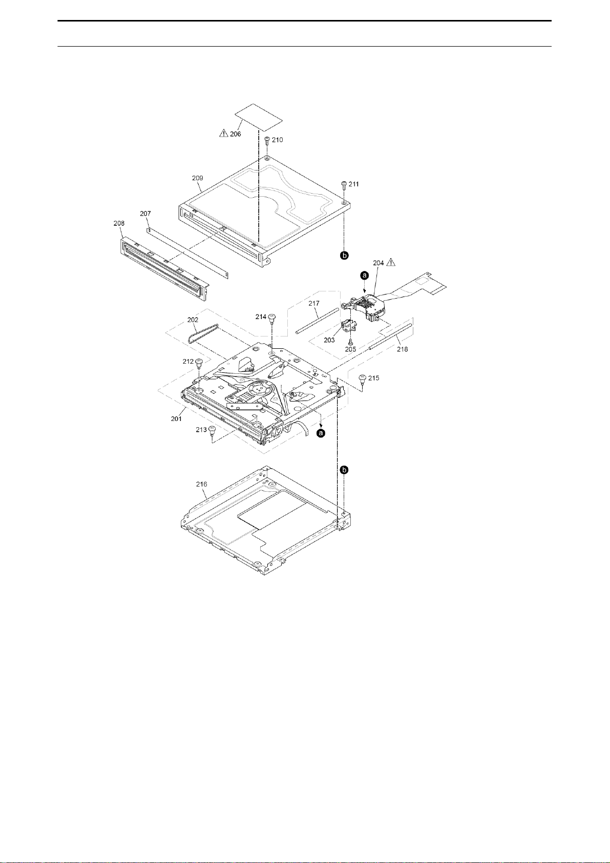
Model No. : DMP-BBT01EG/EB Mechanism Section
Page 98

Model No. : DMP-BBT01EG/EB Packing Parts and Accessories Section
Page 99

Model No. : DMP-BBT01EG/EB Parts List
Safety
Ref.
No.
1 XTN17+6GFJK SCREW 1
2 XTN17+6GFJK SCREW 1
3 XTN17+6GFJK SCREW 1
4 XTN17+6GFJK SCREW 1
5 XTN17+6GFJK SCREW 1
6 RFY0952B-K TOP CASE UNIT 1
7 VEP70552A TOUCH SW P.C.B. UNIT 1 (RTL) E.S.D.
8 RYP1782-K FRONT PANEL UNIT 1
8-1 RMR2083-Q PRISM 1
9 RYF0934-K DOOR UNIT 1
10 RYK1708C-K BOTTOM CASE UNIT 1
10-1 RKA0223-K LEG
10-2 RKA0223-K LEG
10-3 RKA0223-K LEG
10-4 RKA0223-K LEG
12 RMX0490 P.C.B. SPACER 1
13 C5ZZZ0000065 WIRELESS LAN MODULE 1
14 XTB26+4FFJ SCREW 1
15 VEP76301A INPUT DIGI-NET P.C.B. 1 (RTL) E.S.D.
16 XTB26+4FFJ SCREW 1
17 XTB26+4FFJ SCREW 1
18 XTB26+4FFJ SCREW 1
19 XSN3+4FJ SCREW 1
20 XSN3+4FJ SCREW 1
21 XTB26+4FFJ SCREW 1
22 XTB26+4FFJ SCREW 1
23 RXK0714 CHASSIS UNIT 1
24 RMZ1300 BARRIER 1
25 VEP73206C ETHER USB POWER P.C.B. 1 (RTL) E.S.D. EG
25 VEP73206D ETHER USB POWER P.C.B. 1 (RTL) E.S.D. EB
26 VEE1L31 WIRELESS-LAN CABLE UNIT 1
27 RMV0394 DIFFUSED SHEET 1
28 VEP70548A LED BUZZER P.C.B. 1 (RTL) E.S.D.
29 VEP70572A IR LED P.C.B. 1 (RTL) E.S.D.
30 XTB26+4FFJ SCREW 1
31 XTB26+4FFJ SCREW 1
32 VEP76275C BD DIGITAL P. C.B. 1 EG
32 RFKB76275CGT BD DIGITAL P.C.B. 1 EG E.S.D. (JIG AND ADJ.)
32 RFKB76275DBT BD DIGITAL P.C.B. 1 EB E.S.D. (JIG AND ADJ.)
33 XTN26+4FFJ SCREW 1
34 XTN26+4FFJ SCREW 1
35 RMA2381 SIDE ANGLE 1
36 VXY2162 DRIVE UNIT 1
201 VXA9033-SER MECHANISM UNIT(W/O OPU) 1
202 RDV0077 BELT 1
203 VMD6571 NUT PIECE 1
204 RAF3621A-C OPTICAL PICK-UP 1
205 RHD17066-1 SCREW 1
206 VQL2P54 LASER CAUTION LABEL 1
207 VMT2264 TRAY DO OR 1
208 VMD6572 BEZEL 1
209 VXA8993 TOP COVER UNIT 1
210 XTB2+4FFJ SCREW 1
211 XTB2+4FFJ SCREW 1
212 RHD20077 SCREW 1
213 RHD20077 SCREW 1
214 RHD20077 SCREW 1
215 RHD20077 SCREW 1
216 VMA0Y37 UNDER COVER 1
217 RMU0097 SHAFT 1
218 RMU0097 SHAFT 1
A1 K1HY19YY0012 HDMI CABLE 1
Part No. Part Name & Description Q'ty Remarks
Page 100

Model No. : DMP-BBT01EG/EB Parts List
Safety
Ref.
No.
A2 N2QAYB000712 REMOTE CONTROLLER 1 EG
A2 N2QAYB000711 REMOTE CONTROLLER 1 EB
A3 RFEA221W-1AB AC ADAPTOR 1
A4 RJA0043-1C AC POWER SUPPLY CORD 1 EG
A4 K2CT2YY00003 AC POWER SUPPLY CORD 1 EB
A5 VFF0885 CD-ROM (O/I) 1 EG
A6 VQT3W10 OPERATING INSTRUCTIONS 1 EG
A6 VQT3W11 OPERATING INSTRUCTIONS 1 EG
A6 VQT3W24 OPERATING INSTRUCTIONS 1 EB
A7 RFA3406 SET STAND UNIT 1
PC1 RPF0606 POLYETHYLENE COVER 1
PC2 RPQ2927 PAD 1
PC3 RPF0620 POLYETHYLENE COVER 1
PC4 RPN2448A-1 CUSHION A 1
PC5 RPN2448B-1 CUSHION B 1
PC6 RPG0A74 PACKING CASE 1 EG
PC6 RPG0A73 PACKING CASE 1 EB
PC7 RPF0557-1 PE-BAG 1
PC8 RPF0535 POLYETHYLENE COVER 1 EG
PC8 RPF0501 POLYETHYLENE COVER 1 EB
Part No. Part Name & Description Q'ty Remarks
 Loading...