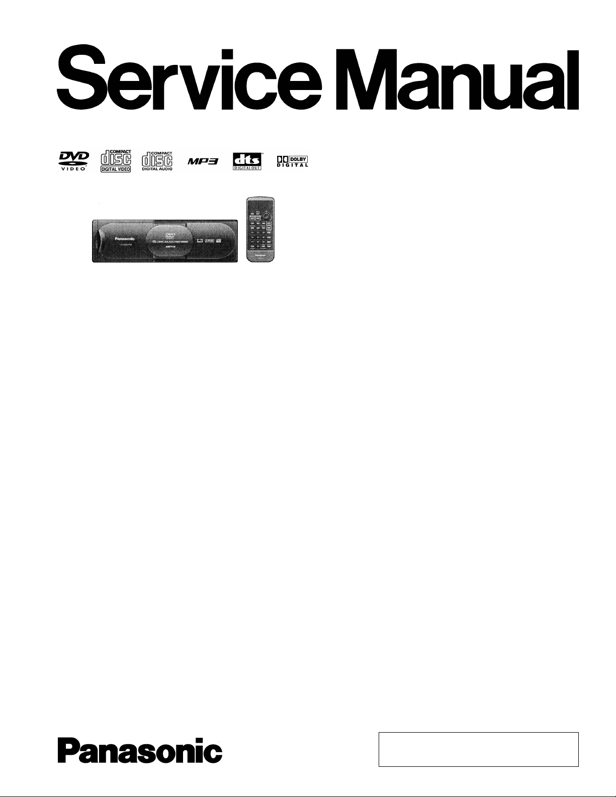
Panasonic CXDH-801-N Service manual
Specifications*
ORDER NO. ACED050312C8
AUTOMOTIVE AFTERMARKET
CX-DH801N
8-Disc DVD Changer
General
Power Supply DC 12V,
Test Voltage 14.4V
Negative Ground
Current Consumption Less than 2.0A (play mode)
DVD Changer Unit
Load Impedance More than 10kΩ
Output Voltage 2V rms (1kHz, 0 dB, at max.)
Output Impedance 600Ω
Channel 2 chanels
Frequency Response 5-20,000Hz±1dB
Signal to Noise Ratio 95dB
Total Harmonic Distortion 0.006% (1,000Hz)
Wow and Flutter Below measurable limit
Light Source Semiconductor laser
Wavelength 650nm
Video section
Video Output Video composite signal, 1.0V
[p-p], 75Ω
Digital audio output
DVD Disc
Sound recording format Optical digital audio output from
connector
Dolby Digital Dolby Digital bitstream (1-5.1 ch)
DTS* DTS bitstream (1-5.1 ch)
(The analog portion is not output)
Linear PCM
(44.1/48/88.2/96 kHz 16/20/24
bit)
MPEG 1 LPCM (48kHz/16bit)
MPEG 2 LPCM (48kHz/16bit)
Video CD
MPEG 1 MPEG 1 bitstream
Linear PCM Linear PCM (2ch)
CD
Linear PCM Linear PCM (2ch)
DTS* DTS bitstream (1-5.1 ch)
*DTS only works with optical outputs.
DVD Changer Unit
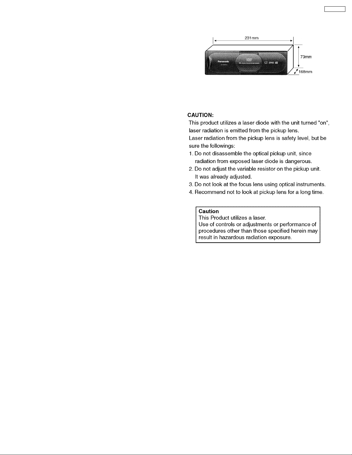
Dimensions (W×H×D)** 231×73×168mm
Weight** 1.5 kg
Disc Magazine Unit : VYQ3174 (included) holds 8 discs
Dimensions (W×H×D)** 121×35×128mm
Weight** 0.2 kg
* Specifications and the design are subject to possible modification
without notice due to improvements.
** Dimensions and Weight shown are approximate.
** Above specifications comply with EIA standards.
Linear PCM (2ch)
(44.1/48/88.2/96 kHz 16/20/24 bit)
(44.1 kHz sampling/16 bit)
(44.1 kHz sampling/16 bit)
(The analog portion is not output)
© 2005 Matsushita Electric Industrial Co., Ltd. All
rights reserved. Unauthorized copying and
distribution is a violation of law.
CX-DH801N
CONTENTS
Page Page
1 ABOUT LEAD FREE SOLDER (PbF) 3
2 FEATURES
3 REPLACING THE FUSE
4 MAINTENANCE
5 NOTES
6 DIMENSIONS
7 LASER PRODUCTS
8 WIRING CONNECTION
9 TERMINALS DESCRIPTION
3
10 IC BLOCK DIAGRAM
11 REPLACEMENT PARTS LIST
3
3
12 EXPLODED VIEW
3
13 WIRING DIAGRAM
14 SCHEMATIC DIAGRAM-1
3
3
15 SCHEMATIC DIAGRAM-2
16 BLOCK DIAGRAM
4
5
8
10
16
18
23
25
27
2
CX-DH801N
1 ABOUT LEAD FREE
SOLDER (PbF)
Distinction of PbF PCB:
PCBs (manufactured) using lead free solder will have a PbF
stamp on the PCB.
Caution :
•
• Pb free solder has a higher melting point than standard
• •
solder; Typically the melting point is 50 - 70°F (30 40°C) higher. Please use a soldering iron with
temperature control and adjust it to 700 ± 20°F (370 ±
10°C). In case of using high temperature soldering iron,
please be careful not to heat too long.
•
• Pb free solder will tend to splash when heated too high
• •
(about 1100°F/600°C)
•
• This lead free solder will be used for the products after
• •
serial No. 1,000,001.
2 FEATURES
•
• DVD Video / Video CD/ CD (CD-DA, MP3) 8 Disc Changer.
• •
•
• Notes
• •
WMA files are not playable.
This unit does not support 8 cm discs.
•
• 5.1-channel system can be buult up.
• •
•
• Both NTSC and PAL format software are playable.
• •
•
• Both NTSC and PAL video format can be generated.
• •
6 DIMENSIONS
7 LASER PRODUCTS
3 REPLACING THE FUSE
Use fuses of the same specified rating (5A). Using different
substitutes or fuses with higher ratings, or connecting the unit
directly without a fuse, could cause fire or damage to the stereo
unit.
4 MAINTENANCE
Your products is designed and manufactured to ensure a
minimum of maintenance. Use a soft cloth for routine exterior
cleaning. Never use benzine, thinner or other solvents.
5 NOTES
[DVD DECK BLOCK]
This model has no servo alignment points because
microcomputer controls the servo circuit
3
CX-DH801N
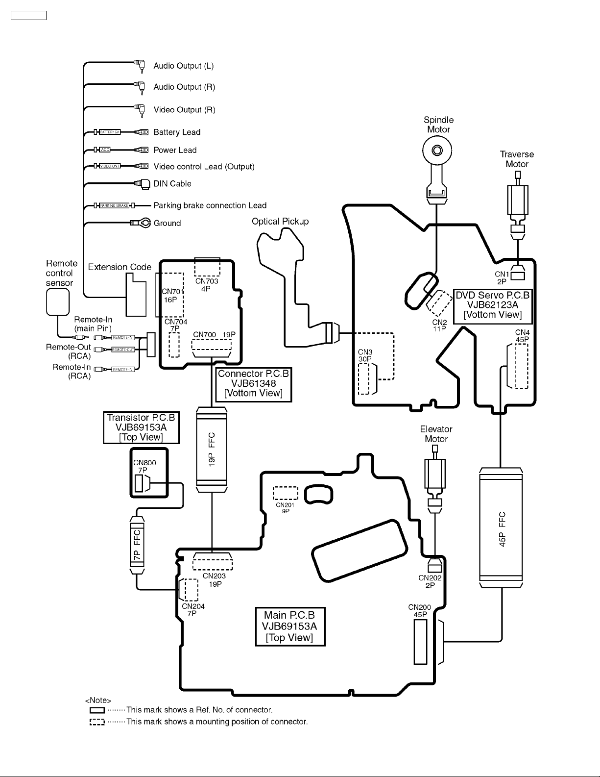
8 WIRING CONNECTION
4
9 TERMINALS DESCRIPTION
CX-DH801N
9.1. Main Block
No. Port Description I/O (V)
1 VD33 1 IO power supply P 3.3
2 XIN X ´tal input (27MHz) I 1.7
3 XOUT X ´tal output (27MHz) O 1.7
4 DCLK System clock I 1.7
5 MA[0] DRAM address 0 O 0
6 MA[1] DRAM address 1 O 0.8
7 MA[2] DRAM address 2 O 0.8
8 MA[3] DRAM address 3 O 1.6
9 VS33 1 IO GND G 0
10 VD33 2 IO power supply P 3.3
11 MA[4] DRAM address 4 O 1.6
12 MA[5] DRAM address 5 O 1.6
13 MA[6] DRAM address 6 O 1.6
14 MA[7] DRAM address 7 O 3.3
15 MA[8] DRAM address 8 O 1.0
16 MA[9] DRAM address 9 O 3.1
17 MA[10] DRAM address 10 O 2.8
18 VS33 2 IO GND G 0
19 VD33 3 IO power supply P 3.3
20 MA[11] DRAM address 11 O 0
21 /CAS DRAM column address strobing O 3.0
22 /CS0 DRAM chip selection 0 O 2.7
23 NC No Connection - 24 /RAS0 DRAM row address strobing 0 O 3.0
25 /RAS1 DRAM row address strobing 1 O 0
26 VSS 1 Internal core GND G 0
27 VDD 1 Internal core power supply P 2.1
28 /RAS2 DRAM row address strobing 2 O 0
29 /DOE DRAM clock enable/output
30 /DWE DRAM write enable O 3.0
31 DB[0] DRAM data 0 I/O 1.2
32 DB[1] DRAM data 1 I/O 1.2
33 DB[2] DRAM data 2 I/O 1.3
34 VS33 3 IO GND G 0
35 VD33 4 IO power supply P 3.3
36 DB[3] DRAM data 3 I/O 1.3
37 DB[4] DRAM data 4 I/O 1.3
38 DB[5] DRAM data 5 I/O 1.0
39 DB[6] DRAM data 6 I/O 1.1
40 DB[7] DRAM data 7 I/O 1.5
41 DB[15] DRAM data 15 I/O 1.7
42 DB[14] DRAM data 14 I/O 1.6
43 VS33 4 IO GND G 0
44 VD33 5 IO power supply P 3.2
45 DB[13] DRAM data 13 I/O 1.3
46 DB[12] DRAM data 12 I/O 1.2
47 DB[11] DRAM data 11 I/O 1.0
48 DB[10] DRAM data 10 I/O 1.2
49 DB[9] DRAM data 9 I/O 1.1
50 DB[8] DRAM data 8 I/O 1.1
51 DSCK DRAM clock O 1.6
52 VS33 5 IO GND G 0
53 VD33 6 IO power supply P 3.3
54 DQM Data IO mask O 0
55 NC No Connection - 56 LA[20] FROM address 20 O 0
57 LA[19] FROM address 19 O 0
58 LA[18] FROM address 18 O 0
59 LA[17] FROM address 17 O 0
60 LA[16] FROM address 16 O 0
61 VS33 6 IO GND G 0
IC203 : C1AB00001972
O 3.3
enable
No. Port Description I/O (V)
62 VD33 7 IO power supply P 3.3
63 LA[15] FROM address 15 O 2.0
64 LA[14] FROM address 14 O 1.3
65 LA[13] FROM address 13 O 2.1
66 LA[12] FROM address 12 O 2.6
67 LA[11] FROM address 11 O 2.2
68 LA[10] FROM address 10 O 0
69 LA[9] FROM address 9 O 2.3
70 VSS 2 Internal core GND G 0
71 VDD 2 Internal core power supply P 2.1
72 LA[8] FROM address 8 O 2.2
73 LA[7] FROM address 7 O 2.4
74 LA[6] FROM address 6 O 1.8
75 LA[5] FROM address 5 O 1.5
76 LA[4] FROM address 4 O 2.2
77 LA[3] FROM address 3 O 2.0
78 VS33 7 IO GND G 0
79 VD33 8 IO power supply P 3.3
80 LA[2] FROM address 2 O 2.0
81 LA[1] FROM address 1 O 2.0
82 LA[0] FROM address 0 O 2.0
83 NC No Connection - 84 NC No Connection - 85 NC No Connection - 86 VSS 3 Internal core GND G 0
87 VDD 3 Internal core power supply P 2.1
88 /LCS3 FROM chip selection O 0
89 /WRLL FROM write enable O 3.3
90 /LOE FROM output enable O 0
91 LD[0] FROM data 0 I/O 1.6
92 LD[1] FROM data 1 I/O 1.6
93 LD[2] FROM data 2 I/O 1.6
94 LD[3] FROM data 3 I/O 0.9
95 VS33 8 IO GND G 0
96 VD33 9 IO power supply P 3.3
97 LD[4] FROM data 4 I/O 1.2
98 LD[5] FROM data 5 I/O 1.8
99 LD[6] FROM data 6 I/O 1.5
100 LD[7] FROM data 7 I/O 1.4
101 NC No Connection - 102 RBCK/TDMCLK Audio cereal clock input I 1.6
103 RWS/TDMFS Audio cereal frame sink input I 1.6
104 VD33 PL PLL power supply P 3.3
105 VS33 PL PLL GND G 0
106 VREF/YUV1 Video DAC VREF/YUV1 output I/O 1.3
107 COMP/YUV3 Video composite input/YUV3
output
108 RSET/YUV4 Input/YUV4 output for DAC
current regulation
109 NC No Connection - 110 VDAC/YUV6 VDAC/YUV6 output O 0
111 VDD33 DA DA power supply P 3.3
112 VS33 DA DA GND G 0
113 NC No Connection - 114 NC No Connection - 115 NC No Connection - 116 TWS PLL audio frame sink
output/<setting>2
117 TSD0 PLL 0 audio serial data
outputs/<setting>0
118 TSD1/SEL PLL1 PLL one audio serial data
output/<setting>1
119 VS33 9 IO GND G 0
120 TSD2 Two audio serial data outputs I/O 0
121 NC No Connection - -
I/O 2.1
I/O 1.3
I/O 1.6
I/O 1.6
I/O 0
5
CX-DH801N
No. Port Description I/O (V)
122 MCLK Clock for audio DAC I/O 1.5
123 TBCK Audio bit clock O 1.6
124 SPD DOBM/SEL
PLL3
S/PDIF output/clock source
switch
I/O 1.6
125 NC No Connection - 126 VD33 10 IO power supply P 0
127 VS33 10 IO GND G 3.3
128 HFMPW High frequency module power
O 0
supply ON (H:ON)
129 DVDSW DVD/CD switch O 0
130 STBY Driver standby O 3.3
131 IP2 Two DVD RAM rivet and bolt
I 0
header outputs
132 IP1 One DVD RAM rivet and bolt
I 0
header output
133 NC No Connection - 134 NC No Connection - 135 NC No Connection - 136 NC No Connection - 137 VSS 4 Internal core GND G 0
138 VDD 4 Internal core power supply P 2.1
139 TEXI High-speed tracking error input I 1.7
140 TESTAD Test AD input I 0
141 SBAD Sub beam input I 2.5
142 FEI Foci error input I 1.5
143 AVSS AD ADC analog GND G 0
144 CEI Central error input I 1.5
145 TEI Tracking error input I 1.5
146 RFRP Radio frequency envelope input I 0
147 AVDD3 AD ADC analog power supply P 3.3
148 VREF21 VREF 2.1V O 2.1
149 VREF09 VREF 0.9V O 0.9
150 VREF15 VREF 1.5V O 1.5
151 IREF PLL current control I 1.2
152 AVDD3 DS Data slice part analog power
P 3.3
supply
153 IPIN Data slice reversing input I 1.5
154 RFIN Radio frequency input (-) I 0
155 RFIP Radio frequency input (+) I 1.5
156 DSSLV Data slice output O 1.5
157 AVSS DS Data slice part GND G 0
158 AVSS PL PLL analog GND G 0
159 PDOFTR1 PLL filter 1 output O 1.5
160 FDO PLL charge pump output O 1.5
161 FTRPOI PLL loop filter input I 1.5
162 AVDD3 PL PLL analog power supply P 3.3
163 NC No Connection - 164 PLLFTR2 PLL loop filter 1 input I 2.1
165 VREFO PLL VREF O 1.5
166 AWRC AWRC DAC I/O 1.9
167 AVSS DA DAC analog GND G 0
168 RFRPCTR RFRP center I/O 1.5
169 NC No Connection - 170 AVDD3 DA Analog power supply in part
P 3.3
DAC
171 SPDRV Spindle output O 1.4
172 FDRV Foci drive output O 1.5
173 NC No Connection - 174 TRSDRY Traverse drive output (-) O 1.4
175 TRDRV Tracking drive output O 1.4
176 NC No Connection - 177 FG FG input I 1.6
178 NC No Connection - 179 SCSJ Chip selection for radio
O 0
frequency setting
180 SDATA Data I/O for radio frequency
I/O 2.2
setting
181 SCLK Clock output for radio frequency
O 3.3
setting
No. Port Description I/O (V)
182 SDFCT DF input I 0
183 SLDC Laser ON/OFF control O 3.3
184 NC No Connection - 185 VD33 11 IO power supply P 3.3
186 VS33 11 IOGND G 0
187 NC No Connection - 188 NC No Connection - 189 CLAMP Chakking completion I 4.9
190 REST Inner detection I 3.3
191 BRK TRV/LD motor brake O 0
192 NC No Connection - 193 EAUX03 - O 3.3
194 EAUX02 General purpose of controlling
I/O 3.3
by servo port 2
195 EAUX01 Audio DAC D 1 I/O 3.3
196 EAUX00 Audio DAC D 0 I/O 0
197 VSS 5 Internal core GND G 0
198 VDD 5 Internal core power supply P 2.1
199 AUX0 FRAMI2C data I/O 3.3
200 AUX1 FRAMI2C Crroc I/O 3.3
201 ACK I/F microcomputer
O 3.3
communication (ACK)
202 NC No Connection - 203 DATAOUT I/F microcomputer
I 4.0
communication (DATAOUT)
204 NC No Connection - 205 STRB I/F microcomputer
I 0
communication (STRB)
206 NC No Connection - 207 /RESET Reset input I 3.3
208 VS33 12 IO GND G 0
6
Pin
Port Description I/O (V)
No.
1 CLMPIN Clamping completion I 0
2 ACCDET ACC voltage detection I 4.9
3 BATDET BATT voltage detection I 4.9
4 P.BRK Parking brake input (L: Parking) I 4.9
IC209 : C2BBFD000510
5 INT Magazine insertion completion
I 5
(L:ON)
6 REST Inner detection SW input (L:ON) I 3.3
7 TEST TEST for treatment device I 4.9
8 TEST C1 C1 for treatment device I 4.9
9 AVSS DGND - 0
10 TEST C2 C2 for treatment device O 4.9
11 ESS RST IC203 DSP reset (L: Reset) O 4.8
12 ACK Dataacc from ESS I 3.3
13 DATAIN Data input from ESS I 3.3
14 E INT External interruption (L:ON) I 0
15 PTDET Elevator position detection I 0
16 SCK Serial clock I 4.9
17 VDD1 Power supply (+5V) - 4.9
18 SI Serial output O 4.9
19 SO Serial input I 4.9
20 TEST DATA Direct access terminal
I/O 4.9
application for treatment device
21 REQ Data transmission demand
O 4.9
(L: Demand)
22 VPP VPP when flash is rewritten - 0
23 XT2(NC) No Connection - 24 XT1 DGND - 0
25 RST Reset (L: Reset) I 4.9
26 X2 Selah lock (10.00MHz) - 3.1
27 X1 Selah lock (10.00MHz) - 2.5
28 VSS0 DGND - 0
29 VDD0 Power supply (+5V) - 4.9
30 MAGCONT Magazine detection
O 4.9
effective/invalidity (H: Effective)
31 PTON Photo sensor ON/OFF (L:ON) O 4.9
32 ELV FWD Rise in elevator O 0
33 ELV REV Descent in elevator O 0
34 SPD1/2 Switch of speed of elevator
O 4.9
(L: High speed)
35 LOD FWD Loading M normal rotation
I/O 1.5
(L: Tray LOAD)
36 MCON Mechanical control ON/OFF
I 0
(L:ON)
37 VSS1 DGND - 0
38 CLMPOUT Clamping completion O 4.9
39 STRB Data strobing to ESS O 4
40 EJECT Eject I 4.9
41 DATAOUT Data output to ESS O 4
42 MAGIN Magazine detection I 0
43 AVDD Power supply (+5V) - 4.9
44 AVREF Power supply (+5V) - 4.9
No.
Port Description I/O (V)
Pin
1 VDD Power supply (+5V) - 4.9
2 GND GND - 0
3 VPP1 VPP when flash is rewritten I 0
4 VDD Power supply (+5V) - 4.9
5 VDD Power supply (+5V) - 4.9
6 GND GND - 0
7 X1 Selah lock (10.00MHz) - 2.1
8 X2 Selah lock (10.00MHz) - 2.3
9 RESET Reset (L: Reset) I 4.7
10 GND DGND - 0
11 NC No Connection - 12 MCON Mechanical control (L: Operation) O 0
13 NC GND O 0
14 NC GND O 0
IC211 : C2BBGD000090
15 REQ Data communication demand
I 4.9
(L: Demands)
16-22 NC GND O 0
23 MCRST Mechanical riset output
O 4.9
(L: Reset)
24 PON Power supply control O 4.9
25 SO Mechanical control
O 4.9
communication serial output
26 SI Mechanical control
I 4.9
communication serial input
27 SCK Mechanical control
I/O 4.9
communication clock output (at
flash rewritten : Input)
28 NC GND O 0
29 NC GND O 0
30 NC GND - 0
31 NC GND - 0
32 GND GND - 0
33 VDD Power supply (+5V) - 4.9
34 REMO - O 5.0
35 NC GND O 0
36 CLK Clock output for communication O 4.8
37 REMO Data input for communication I 5.0
38 DATA Data output for communication O 4.3
39 IR Remote control input I 5.0
40 NC GND I 0
41 A/D Changer 1/2 switch (H:1) I 4.9
42 STB Strobing output for
O 0
communication
43 P.BRK Parking brake input (H: Parking) I 0
44 VIDEO CNT Video control O 4.9
45-56 NC GND O 0
57 BATDET Battery voltage detection I 4.8
58 ACCDET ACC voltage detection I 4.8
59-64 NC GND I 0
CX-DH801N
7
CX-DH801N
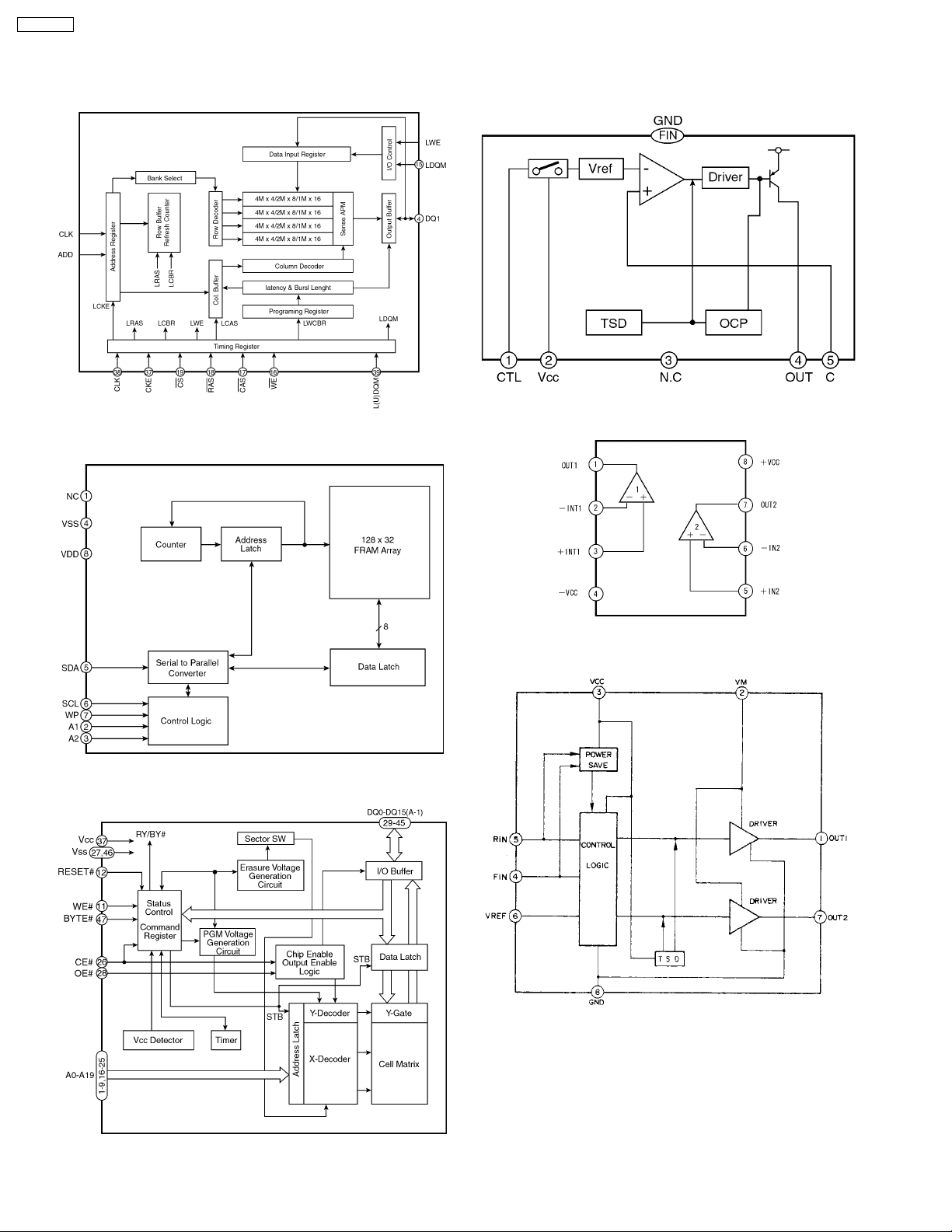
10 IC BLOCK DIAGRAM
10.1. Main Block
IC200 : C3ABPG000133
IC206 : C0DBEJG00001
IC202 : C3GBBC000007
IC208 : C0ABBB000220
IC210 : C0GBD0000010
IC204 : C3FBMD000216
8
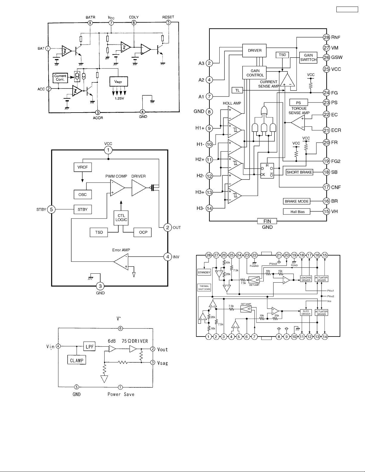
IC212 : AN8065SE1
CX-DH801N
10.2. DVD Servo Block
IC215 : C0DBAZG00033
IC218 : C1AB00001756
IC1 : C0GBF0000004
IC2 : C0GBE0000004
9
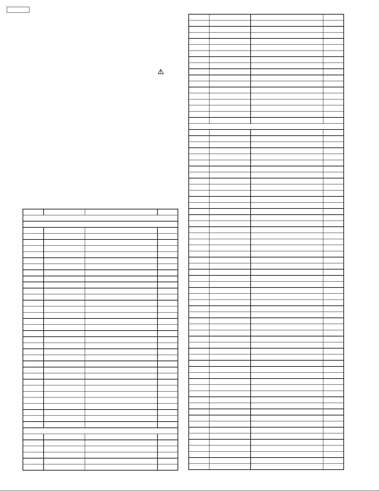
CX-DH801N
11 REPLACEMENT PARTS
LIST
Notes :
1. Be sure to make your orders of replacement parts
according to this list.
2. Important safety notice: Components, identified by
have special characteristics important for safety. When
replacing any of these components, use only
manufacturer´s specified parts.
3. Location keys in the remarks column indicates the general
location of the parts shown in the exploded drawing, as in a
road map.
4. The marking (RTL) indicates that Retention Time is limited
for this item. After the discontinuation of assembly in
production, the item will continue to be available for a
specific period of time. The retention period of availability is
dependent on the type of assembly, and in accordance with
the laws governing part and product retention. After the end
of this period, the assembly will no longer be available.
•
• Order intake period is basically six months after the first
• •
shipment.
5. “T” marks in remarks colum are indicated supply parts of
TAMACO.
Ref. No. Part No. Part Name & Description Remarks
[VJB69153A] Main/Transistor Block
IC´s AND TRANSISTORs
IC200 C3ABPG000133 IC
IC202 C3GBBC000007 IC
IC203 C1AB00001972 IC
IC204 C3FBMD000216 IC
IC206 C0DBEJG00001 IC
IC208 C0ABBB000220 IC
IC209 C2BBFD000510 IC
IC210 C0GBD0000010 IC
IC211 C2BBGD000090 IC
IC212 AN8065SE1 IC
IC213 C0JBAB000406 IC
IC215 C0DBAZG00033 IC
IC216 C0FBBK000057 IC
IC217 C0JBAA000099 IC
IC218 C1AB00001756 IC
IC219 C0EBE0000340 IC
Q200 2SB07100RL Transistor
Q201 B1ABGC000005 Transistor
Q202 B1ABGC000005 Transistor
Q203 B1GDCFGN0001 Transistor
Q204 YEANC114YKX Transistor
Q205 B1BCCG000002 Transistor
Q206 B1BBAC000007 Transistor
Q207 YEANFP1F3PT1 Transistor
Q208 B1GBCFNN0004 Transistor
Q209 B1GKCFGJ0001 Transistor
Q218 B1GDCFGN0001 Transistor
Q220 B1BBCD000001 Transistor
Q221 B1GBCFNN0004 Transistor
Q222 B1ABGC000005 Transistor
ZC1 YEANRPI352 Transistor
DIODEs
D207 B0ACCK000005 Diode
D208 B0BC8R100004 Diode
D209 B0JCCE000002 Diode
D211 B0BC5R600003 Diode
D213 YEADSR1544TL Diode
D215 B0JCPE000003 Diode
mark
Ref. No. Part No. Part Name & Description Remarks
D216 B0ACCK000005 Diode
D218 B3ABA0000337 Diode
D219 B0BC5R600003 Diode
D220 MA3J14300L Diode
D221 B0JCCE000002 Diode
D222 B0JCCE000002 Diode
D223 B0JCCE000002 Diode
D224 YEADRB081L20 Diode
D225 YEADRB081L20 Diode
D226 B0BC5R600003 Diode
D227 B0BC5R600003 Diode
D228 B0BC8R100004 Diode
D230 B0BC4R0A0006 Diode
D235 YEADRB081L20 Diode
D236 YEADRB081L20 Diode
CAPACITORs
C200 ECJ1VF1C105Z Ceramic, 1µF 16WV
C201 ECJ1VF1C105Z Ceramic, 1µF 16WV
C202 ECJ1VF1C105Z Ceramic, 1µF 16WV
C203 ECJ1VF1C105Z Ceramic, 1µF 16WV
C204 F1H1C104A009 Ceramic, 0.1µF 16WV
C205 EEEHB1C100R 10µF 16WV
C207 F1H1C104A042 Ceramic, 33PF 50WV
C208 ECJ1VC1H330J Ceramic, 47PF 50WV
C209 ECJ1VC1H470J Ceramic, 33PF 50WV
C210 F1H1C104A042 Ceramic, 0.1µF 16WV
C211 ECJ1VC1H330J Ceramic, 1µF 16WV
C212 ECJ1VF1C105Z Ceramic, 1µF 16WV
C215 F1H1C473A054 Ceramic, 0.047µF 16WV
C216 ECJ1VB1H561K Ceramic, 560PF 50WV
C217 ECJ1VC1H330J Ceramic, 33PF 50WV
C218 F1H1C104A009 Ceramic, 0.1µF 16WV
C219 F1H1C104A009 Ceramic, 0.1µF 16WV
C220 F1H1C104A009 Ceramic, 0.1µF 16WV
C221 ECJ1VF1C105Z Ceramic, 1µF 16WV
C222 ECJ1VF1C105Z Ceramic, 1µF 16WV
C223 ECJ1VF1C105Z Ceramic, 1µF 16WV
C224 F1H1C104A042 Ceramic, 0.1µF 16WV
C225 ECJ1VC1H080D Ceramic, 8PF 50WV
C227 ECJ1VB1H472K Ceramic, 4700PF 50WV
C229 F1H1C104A009 Ceramic, 0.1µF 16WV
C230 ECJ1VB1H472K Ceramic, 4700PF 50WV
C231 ECJ1VF1C105Z Ceramic, 1µF 16WV
C232 ECJ1VC1H080D Ceramic, 8PF 50WV
C233 ECJ1VB1H682K Ceramic, 6800PF 50WV
C234 F1H1H102A009 Ceramic, 1000PF 50WV
C235 ECJ1VB1H472K Ceramic, 4700PF 50WV
C236 F1H1H102A009 Ceramic, 1000PF 50WV
C237 F1H1H102A009 Ceramic, 1000PF 50WV
C238 F1H1H102A009 Ceramic, 1000PF 50WV
C239 F1H1C104A042 Ceramic, 0.1µF 16WV
C240 EEEHB1E4R7R 4.7µF 25WV
C241 ECJ1VF1C105Z Ceramic, 1µF 16WV
C242 ECJ1VF1C105Z Ceramic, 1µF 16WV
C243 ECJ1VF1C105Z Ceramic, 1µF 16WV
C244 ECJ1VF1C105Z Ceramic, 1µF 16WV
C245 ECJ1VF1C105Z Ceramic, 1µF 16WV
C246 ECJ1VF1C105Z Ceramic, 1µF 16WV
C247 F1H1C104A042 Ceramic, 0.1µF 16WV
C248 ECJ1VF1C105Z Ceramic, 1µF 16WV
C249 ECJ1VF1C105Z Ceramic, 1µF 16WV
C250 ECJ1VF1C105Z Ceramic, 1µF 16WV
C251 ECJ1VF1C105Z Ceramic, 1µF 16WV
C252 ECJ1VF1C105Z Ceramic, 1µF 16WV
C253 F1H1C104A042 Ceramic, 0.1µF 16WV
C254 ECJ1VB1H331K Ceramic, 330PF 50WV
C255 ECJ1VC1H121J Ceramic, 120PF 50WV
C256 F1H1C104A009 Ceramic, 0.1µF 16WV
C257 ECJ1VC1H680J Ceramic, 68PF 50WV
C258 EEFCD0G680R Electrolytic, 68µF 4WV
C259 F1H1C104A009 Ceramic, 0.1µF 16WV
C260 F1K1A1060015 Ceramic, 10µF 10WV
10
 Loading...