

Page 1
ORDER NO. MTNC020827A1
B1
Service Manual
Color Television
d
S
m
i
p
l
i
f
i
e
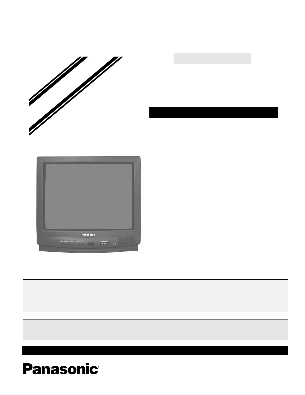
Simplified Manual
(NA7D)
Panasonic
Models
CT-2022HBF AP395
CT-2022HBCF AP395
Chassis
This simplified service manual is issued to add the models of the NA7D family listed above to main manual order No.
MTNC010734C1 (CT-2022HE). Included in this simplified service manual are unique characteristics and a complete
parts list. Please file and use together with the main service manual order No. MTNC010734C1 (CT-2022HE) and
related manuals.
“WARNING! This service manual isdesigned forexperienced repair techniciansonly and is not designed for use by the generalpublic.
It does not contain warnings or cautions to advise non-technical individuals of potential dangers in attempting to service a product.
Products poweredby electricity should be serviced or repaired only by experienced professional technicians. Any attempt to
service or repair the product or products dealt with in this service manual by anyone else could result in serious injury or death.”
The service technician is requiredtoreadand follow the “Safety Precautions”and“Important Safety Notice” in this Manual.
Copyright2002 by Matsushita Electric Corporationof
America. All rights reserved. Unauthorized copying
and distribution is a violation of law.
Page 2
Important safety notice
Special components are used in this television set which are important for safety. These parts are identified on the
schematic diagram by the symbol and printed in BOLD TYPE on the replacement part list. It is essential that
these critical parts are replaced with the manufacturer’s specified replacement part to prevent X-ray radiation,
shock, fire or other hazards. Do not modify the original design without the manufacturer’s permission.
Safety precautions
General guidelines
An isolation transformer should always be used
during the servicing of a Receiver whose chassis is not
isolated from AC power line. Use a transformer of
adequate power rating as this protects the technician
from accidents resulting in personal injury from
electrical shocks. It will also protect the Receiver from
being damaged by accidental shorting that may occur
during servicing.
When servicing, observe the original lead dress,
especially in the high voltage circuit. Replace all
damaged parts (also parts that show signs of
overheating.)
Always replace protective devices,suchas
fishpaper, isolation resistors and capacitors, and
shields after servicing the Receiver. Use only
manufacturer’s recommended rating for fuses, circuits
breakers, etc.
High potentials are present when this receiver is
operating. Operation of the receiver without the rear
cover introduces danger for electrical shock. Servicing
should not be performed by anyone who is not
thoroughly familiar with the necessary precautions
when servicing high-voltage equipment.
Extreme care should be practiced when handling the
picture tube. Rough handling may cause it to implode
due to atmospheric pressure. (14.7 lbs per sq. in.). Do
not nick or scratch the glass or subject it to any undue
pressure. When handling, use safety goggles and
heavy gloves for protection. Discharge the picture
tube by shorting the anode to chassis ground (not to
the cabinet or to other mounting hardware). When
discharging connect cold ground (i.e. dag ground lead)
to the anode with a well insulated wire or use a
grounding probe.
Avoid prolonged exposure at close range to unshielded
areas of the picture tube to prevent exposure to X-ray
radiation.
The test picture tube used for servicing the chassis at
the bench should incorporate safety glass and
magnetic shielding. The safety glass provide shielding
for the tube viewing area against X-ray radiation as
well as implosion. The magnetic shield limits the X-ray
radiation around the bell of the picture tube in addition
to the restricting magnetic effects. When using a
picture tube test jig for service, ensure that the jig is
capable of handling 50kV without causing X-ray
radiation.
Before returning a serviced receiver to the owner,
the service technician must thoroughly test the unit to
ensure that is completely safe to operate. Do not use a
line isolation transformer when testing.
Leakage current cold check
Unplug the AC cord and connect a jumper between the
two plug prongs.
Measure the resistance between the jumpered AC plug
and expose metallic parts such as screwheads,
antenna terminals, control shafts, etc. If the exposed
metallic part has a return path to the chassis, the
reading should be between 240kΩ and 5.2MΩ. If the
exposed metallic part does not have a return path to
the chassis, the reading should be infinite.
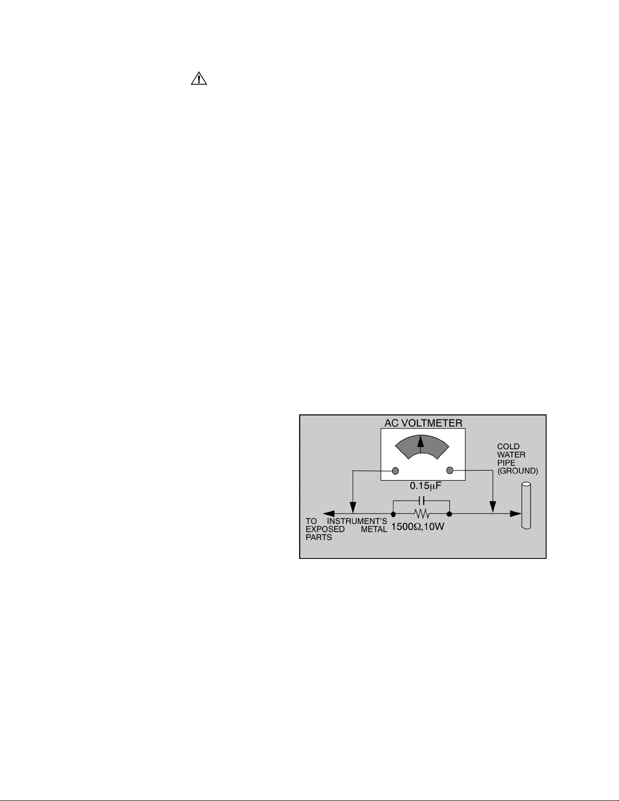
Leakage current hot check (Fig. 1)
Plug the AC cord directly into the AC outlet. Do not use
an isolation transformer during the check.
Connect a 1.5kΩ 10 watt resistor in parallel with a
0.15µF capacitor between an exposed metallic part
and ground. Use earth ground, for example a
water pipe.
Using a DVM with a 1000 ohms/volt sensitivity or
higher, measure the AC potential across the resistor.
Repeat the procedure and measure the voltage
present with all other exposed metallic parts.
Verify that any potential does not exceed 0.75 volt
RMS. A leakage current tester (such a Simpson Model
229, Sencore Model PR57 or equivalent) may be used
in the above procedure, in which case any current
measure must not exceed 0.5 milliamp. If any
measurement is out of the specified limits, there is a
possibility of a shock hazard and the Receiver must be
repaired and rechecked before it is returned to the
customer.
Figure 1. Hot check circuit
X-ray radiation
WARNING: The potential source of X-ray radiation in the
receiver isin the high voltagesectionand the picture tube.
Refer to “X-Ray protection circuit check & adjustments”
on page 6 to confirm HHS voltage.
High voltage (CRT anode)
Set the brightness, picture, sharpness and color
controls to minimum (to obtain dark image). Measure
the High Volt age. The high voltage should be
27.70kV ± 1.25kV . If the upper limit is out of tolerance,
immediate service and correction is required.
Note: It is important to use an accurate, calibrated
high voltage meter.
-2-
Page 3
About lead free solder (PbF)
Note: Lead is listed as (Pb) in the periodic table of elements.
In the information below, Pb will refer to Lead solder, and PbF will refer to Lead Free Solder.
The Lead Free Solder used in our ma nufacturing process and discussed below is (Sn+Ag+Cu).
That is Tin (Sn), Silver (Ag) and c opper (Cu) although other types ar e available.
This model uses Pb Free solder in it’s manufacture due to environmental conservation issues. For
service and repair work, we’d suggest the use of Pb free solder as well, although Pb solder may be
used.
PCBs manufactured using lead free solder will have the “PbF” or a leaf symbol stamped on the
back of PCB.
Caution
• Pb free solder has a higher melting point than standard solder. Typically the melting
point is 50 ~ 70 °F(30~40°C) higher. Please use a high temperature soldering iron
and set it to 700 ± 20 °F(370± 10 °C).
• Pb free solder will tend to splash when heated too high (about 1100 °For600°C).
If you must use Pb solder, please completely remove all of the Pb free solder on the
pins or solder area before applying Pb solder. If this is not practical, be sure to heat the
Pb free solder until it melts, before applying Pb solder.
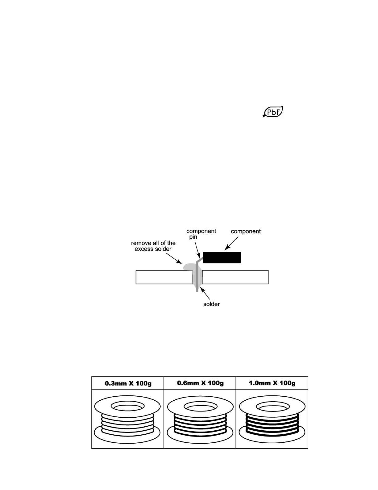
• After applying PbF solder to double layered boards, please check the component side
for excess solder which may flow onto the opposite side. (see figure below)
slice view
Suggested Pb free solder
There are several kinds of Pb free solder available for purchase. This product uses Sn+Ag+Cu
(tin, silver, copper) solder. However, Sn+Cu (tin, copper), Sn+Zn+Bi (tin, zinc, bismuth) solder
canalsobeused.
-3-
Page 4

Importantsafetynotice ...................2
Safetyprecautions..................2
Generalguidelines..................2
Leakagecurrentcoldcheck...........2
Leakagecurrenthotcheck ...........2
X-rayradiation.....................2
High voltage (CRT anode). . . . ........2
Servicenotes ...........................5
Leadless chip component
(surfacemount)....................5
Componentremoval ................5
Chip component installation . . ........5
Howtoreplaceflat-IC...............5
X-ray protection circuit check
&adjustments..................6
Locationofcontrols(Remote) .............9
Identification of components . . . . . . .......10
Audiosignalpathblockdiagram ..........12
Videosignalpathblockdiagram...........13
Partslist ..............................14
Components abbreviations guide. . . .......19
Schematicnotes........................20
A-Boardschematic.......................22
C-Boardschematic.......................27
-4-
Page 5
Service notes
Note: Some components may be affixed with glue. Be careful not to break or damage foil under the component
or at the pins of the ICs when removing. Usually applying heat to the component for a short time while
twisting with tweezers will break the component loose.
Leadless chip component
(surface mount)
Chip components must be replaced with identical chips
due to critical foil track spacing. There are no holes in
the board to mount standard transistors or diodes.
Some chips capacitor or resistor board solder pads
may have holes through the board, however the hole
diameter limits standard resistor replacement to 1/8
watt. Standard capacitor may also be limited for the
same reason. It is recommended that identical
components be used.
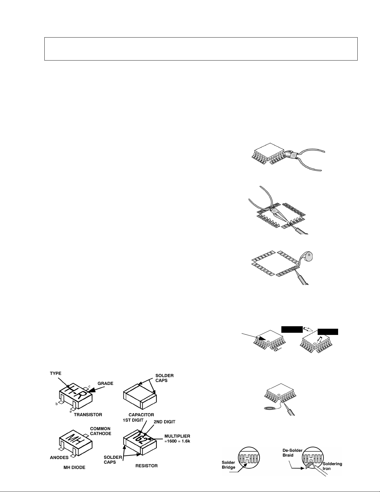
Chip resistor have a three digit numerical resistance
code - 1st and 2nd significant digits and a multiplier.
Example: 162 = 1600 or 1.6kΩ resistor, 0 = 0Ω (jumper).
Chip capacitors generally do not have the value
indicated on the capacitor. The color of the component
indicates the general range of the capacitance.
Chip transistors are identified by a two letter code. The
first letter indicates the type and the second letter, the
grade of transistor.
Chip diodes have a two letter identification code as per
the code chart and are a dual diode pack with either
common anode or common cathode. Check the parts
list for correct diode number.
Component removal
1. Use solder wick to remove solder from component
end caps or terminal.
2. Without pulling up, carefully twist the component
with tweezers to break the adhesive.
3. Do not reuse removed leadless or chip
components since they are subject to stress
fracture during removal.
Chip component installation
1. Put a small amount of solder on the board
soldering pads.
2. Hold the chip component against the soldering
pads with tweezers or with a miniature alligator clip
and apply heat to the pad area with a 30 watt iron
until solder flows. Do not apply heat for more than
3 seconds.
Chip components
How to replace flat-IC
- Required Tools -
• Soldering iron • De-solder braids
• Needle nose pliers • Magnifier
• Wire cutters (sharp & small)
1. Cut the pins of a defective IC with wire cutters.
Remove IC from board. If IC is glued to the board,
heat the IC and release the IC. See Note above.
Flat IC
2. Using soldering iron and needle nose pliers
remove the IC pins from the board.
Soldering
Iron
3. Using de-soldering braid and soldering iron remove
solder from affected are on board (pads).
De-soldering
Braid
Soldering
Iron
4. Position the new Flat-IC in place (apply the pins of
the Flat-IC to the soldering pads where the pins
need to be soldered). Determine the positions of
the soldering pads and pins by correctly aligning
the polarity symbol. Solder pin #1 first, align the IC.
Polarity
symbol
Solder the pin opposite to pin #1. This will assist
positioning the IC.
5. Solder all pins to the soldering pads using a fine
tipped soldering iron.
2nd solder
1st solder
Solder
6. Check with a magnifier for solder bridge between
the pins or for dry joint between pins and soldering
pads. To remove a solder bridge, use a de-solder
braid as shown in the figure below.
-5-
Soldering
Iron
Page 6
IMPORTANT: To protect against possible damage to
the solid state devices due to arcing or static discharge,
make certain that all ground wires and CRT DAG wire
are securely connected.
CAUTION: The power supply circuit is above earth
ground and the chassis cannot be polarized. Use an
isolation transformer when servicing the Receiver to
avoid damage to the test equipment or to the chassis.
Connect the test equipment to the proper ground ( ) or
( ) when servicing, or incorrect voltages will be
measured.
WARNING: This Receiver has been designed to meet
or exceed applicable safety and X-ray radiation
protection as specified by government agencies and
independent testing laboratories.
To maintain original product safety design standards
relative to x-ray radiation and shock and fire hazard,
parts indicated with the symbol on the schematic
must be replaced with identical parts. Order parts from
the manufacturer’s parts center using the parts
numbers shown in this service manual, or provide the
chassis number and the part reference number.
For optimum performance and reliability, all other parts
should be replaced with components of identical
specification.
X-Ray protection circuit check &
adjustments
This test must be performed as final check before the
Receiver is returned to the customer. If voltages are out
of tolerance, immediate service and correction is
required to insure safe operation and to prevent the
possibility of premature component failure.
Equipment:
1. Isolation transformer.
2. High voltage meter.
3. Short jumper.
4. Jumper diode (same as D823, PN S3L60P154004).
diode should be rated a minimum of 150V.
Procedure:
1. Connect the receiver to an isolation transformer.
turn receiver ON.
2. Apply a monoscope pattern.
3. In service mode (see service mode section in this
manual) select register C0B.
4. Measure TP5 (located near the tuner). Compare
the measured value to the left column of the table
below. Set C0B with value from the right column
corresponding to the measured level at TP5.
Example, if the measured level at TP5 is 1.03V, set
C0B to 03.
TP5 MEASUREMENT SET C0B TO (HEX)
0 ~ 0.93V 00
0.93 ~ 0.97V 01
0.97 ~ 1.01V 02
1.01 ~ 1.05V 03
1.05 ~ 1.09V 04
1.09 ~ 1.13V 05
1.13 ~ 1.17V 06
1.17 ~ 1.21V 07
5. Exit service mode and shut it OFF .
6. Connect the short jumper between TPD16 and
TPD17.
7. Connect the jumper diode between TPD14 and
TPD15 (cathode connected to TPD14, anode
connected to TPD15).
8. Apply 75VAC to the input of the isolation
transformer.
9. Turn receiver ON.
10. Set PICTURE and BRIGHTNESS to minimum.
11. Slowly increase the voltage at the input of the
isolation transformer and confirm HHS voltage
measure 34.0KV when the receiver starts to go out
of sync.
12. Turn receiver OFF and remove jumper & diode.
-6-
Page 7
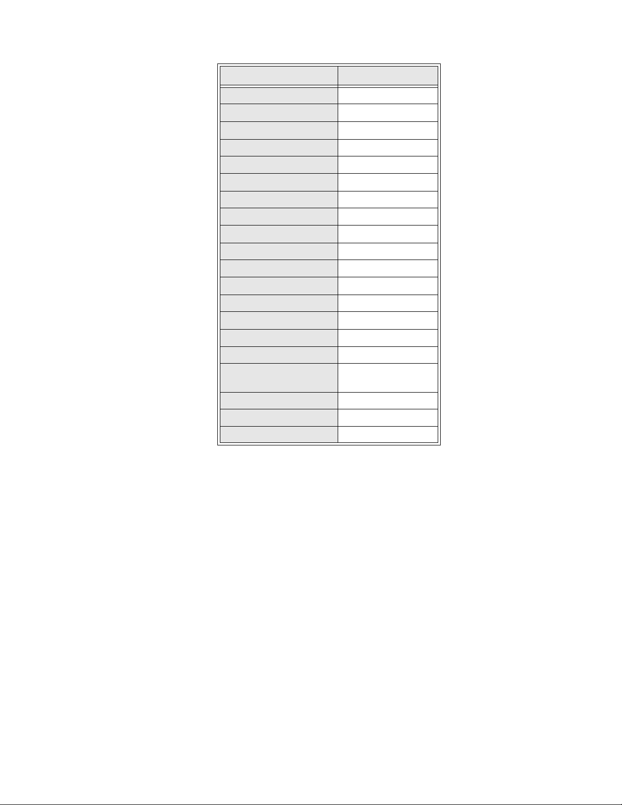
Receiver feature table
FEA TURE/MODEL CT-2022HBF/HBCF
Chassis AP395
Tuning system
Number of channels 181
Closed Caption X
V-Chip X
75 Ω input X
Remote TV Only EUR501450
CRT SUPPLIER BMCC
Comb filter 2Dig
V/A norm (X=BOTH) V
AUTO ON X
AI Sound (always on) X
Built-in audio power 1.5W
Number of speakers 1
A/V in (rear/front) (0/1)
Smart plug interfase SMART PLUG
Dimensions mm
(HxWxD) in
Weight (kg/lbs) 19.7/43.34
40K - GEN
516x492x462
20.28x19.33x18.15
II
Power source (V/Hz) 120/60
Anode voltage 27.7kV±1.25kV
Table 1. Receiver features
-7-
Page 8

Board description
BOARD CT-2022HBF/HBCF DESCRIPTION
A-Board TNP2AH024 DZ MAIN BOARD
C-Board TNP2AA075 AH CRT BOARD
DI-Board TNP2AA094 NIL SMART PLUG
Table 1. Receiver features
Specifications are subject to change without notice or obligation.
Dimensions and weights are approximate.
Note: When ordering a replacement board, append an “S” to
the board number.
Example: to order the A-Board for CT-2022HBF, the
replacement board is TNP2AH024DZS.
-8-
Page 9
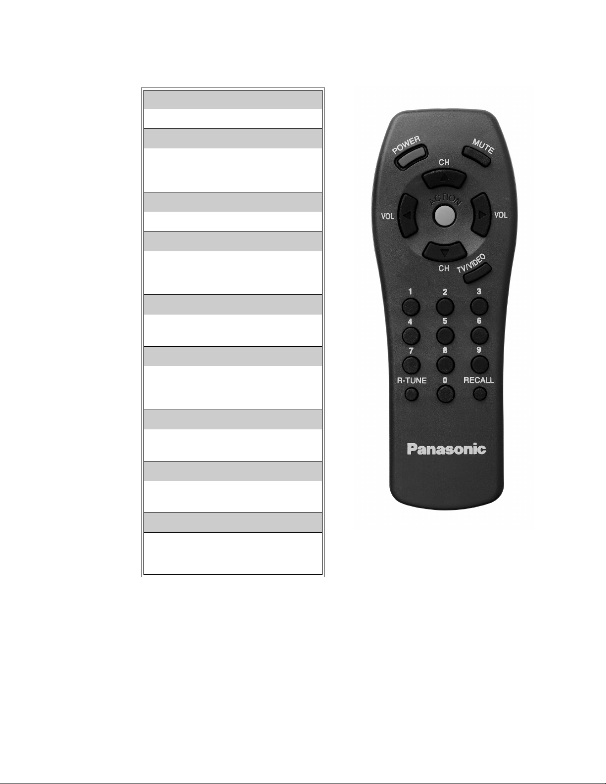
Location of controls (remote)
POWER button
Press to turn ON and OFF.
MUTE button
Press to mute sound. A second press
resumes sound. Press also to access
and delete closed caption display.
TV/VIDEO button
Press to select TV or Video input.
VOLUME buttons
Press to adjust TV sound level. Use
with channel buttons to navigate in
menus.
CHANNEL buttons
Press to select channels. Use with
volume buttons to navigate in menus.
ACTION button
Press to display main menu and
access or exit on screen features and
adjustment menus.
Keypad buttons
Press desired channel number to
randomly access any channel.
R-TUNE (rapid tune) button.
Press to switch to the previous
channel.
RECALL button
Press to display time, status of sleep
timer, channel, video mode and
channel caption (station identifier).
Figure 2. Location of controls (remote).
EUR501450
-9-
Page 10
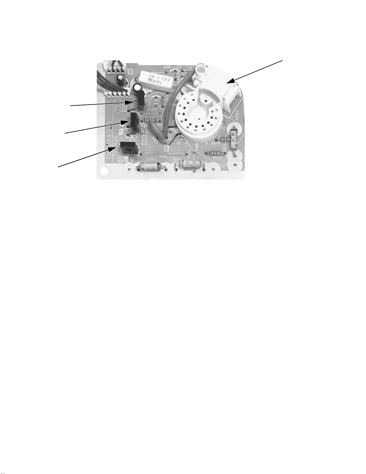
Q352
Gout
Q353
Bout
Identification of components
CRT socket
Q351
R out
Figure 3. C-Board components location
-10-
Page 11
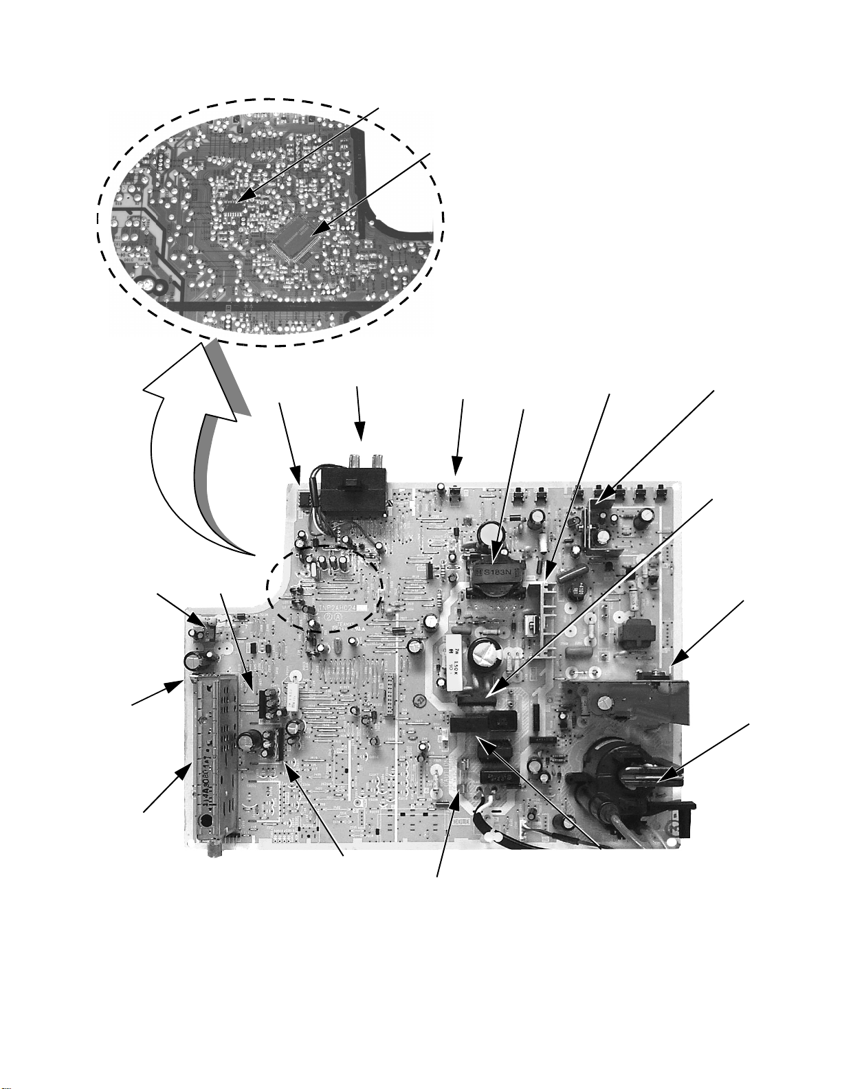
Identification of components
IC050
halftone
IC001
MPU
Components on trace side
IC552
Stand-By
Reg
IC551
9V Reg
IC2401
IC002
Front A/V
jacks
IC003
T801
Chopper
Transformer
IC801
IC451
D801
Q551
Flyback
T551
TNR001
IC2302
F801
Figure 4. A-Board location of components
-11-
RL801
Page 12
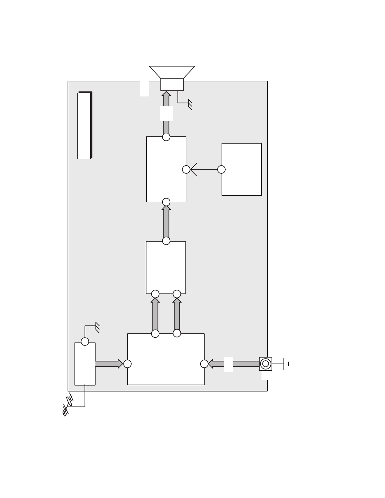
Audiosignalpathblockdiagram
-
+
SPEAKER
OUT
LEFT
10
A-BOARD
OUT
LEFT
L IN
1
9
OUT
IC2302
L/MONO
TV
IN
3
3
L
OUT
IC2401
VOL
R IN
10
10
OUT
6
64
VOL
IC001
MPU/VCJ
TUNER
TNR001
8
AUDIO IN
AUDIO
IC3101
SWITCH
IN
LEFT
11
Figure 5. Audio signal block diagram
-12-
LEFT
A1
AUDIO
FRONT
JK3001
Page 13
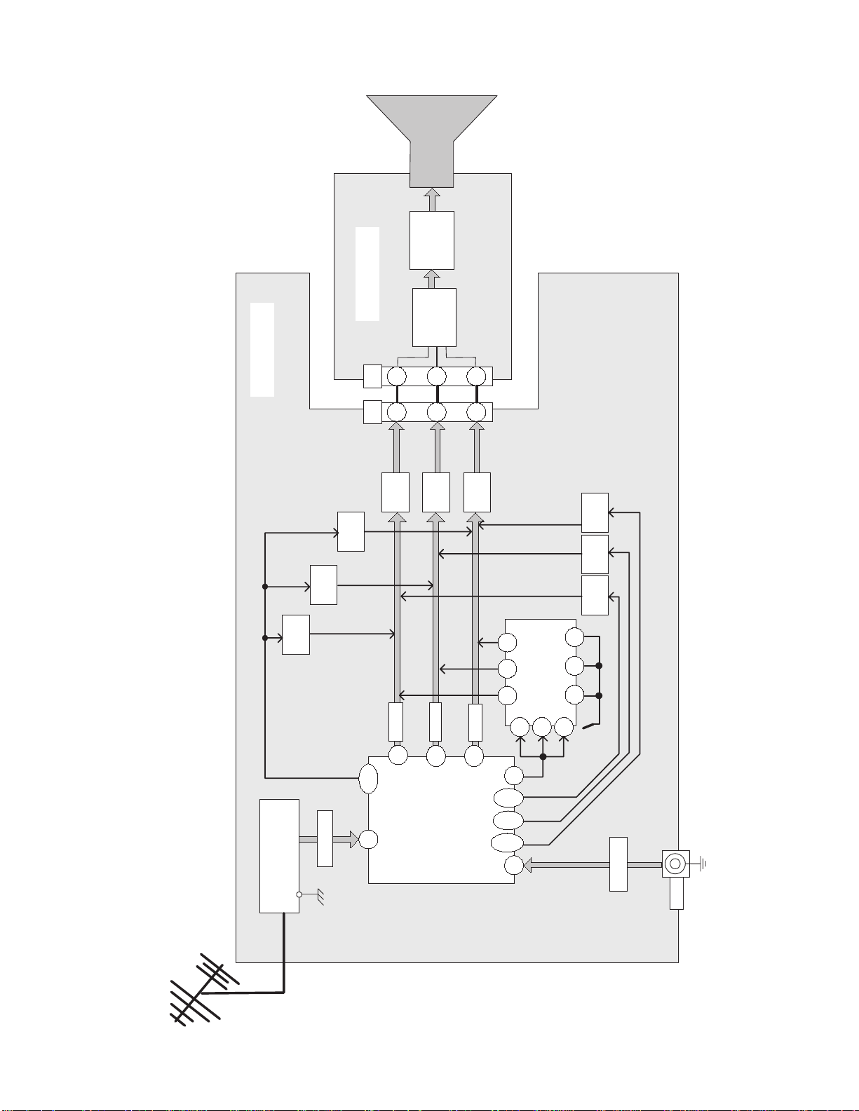
Videosignalpathblockdiagram
Q353 -B
Q351 -R
Q352 -G
C-BOARD
Q356 -B
Q354 -R
Q355 -G
1
2
A-BOARD
C1
A11
1
3
2
3
Q053
TNR001
MAIN TUNER
Q054
VIDEO IN
Q055
50,56
26
Q006
R-OUT
28
FB
TV IN
Q007
G-OUT
30
IC001
MPU/VCJ
Q008
B-OUT
32
HALF-
RGB
OSD
41 8
59
TONE
55,
51
57,
49
58,
48
20
EXT
5
IC050
HALFTONE
6
13
Q050 Q051 Q052
2 3 9
3.3V
VIDEO IN
V 1
JK3001
FRONT VIDEO
Figure 6. Video signal block diagram
-13-
Page 14
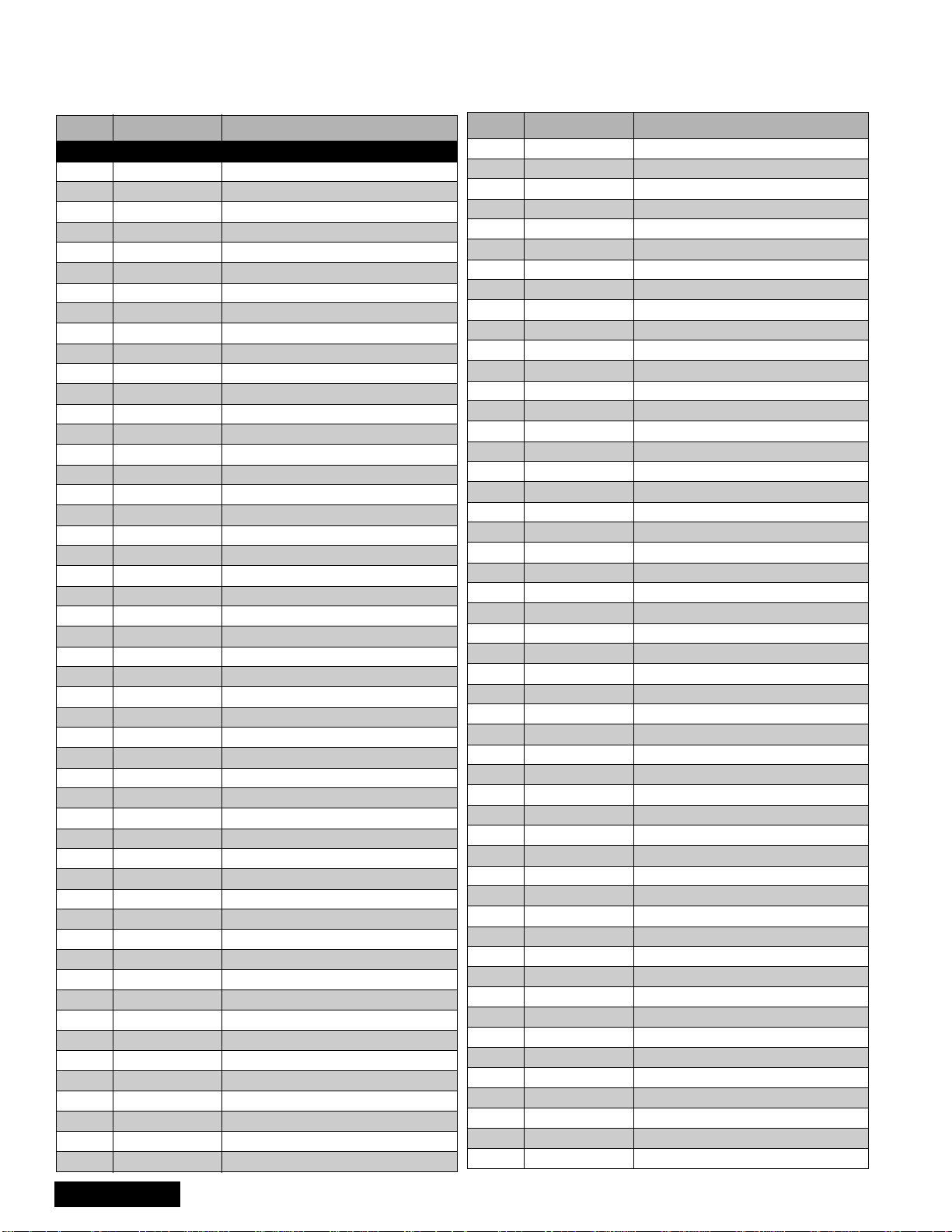
REPLACEMENT PARTS LIST
Models: CT-2022HBF, CT-2022HBCF.
Important Safety Notice: Components printed in BOLD TYPE have special c haracteristics important for safety. When replacing
any of these components use only manufacturer’s specified parts.
REF NO. PART NO. DESCRIPTION
CAPACITORS
C001 TCJ2VB1H103K CAP,C .01UF-K-50V
C002 TCJ2VB1H471K CAP,C 470PF-K-50V
C003 ECA1HM4R7B CAP,E 4.7UF-50V
C004 TCJ2VC1H150J CAP,C 15PF-J-50V
C005 TCJ2VC1H150J CAP,C 15PF-J-50V
C008 TCJ2VF1H104Z CAP,C .1UF-Z-50V
C009 ECA1CM470B CAP,E 47UF/16V
C010 TCJ2VF1H104Z CAP,C .1UF-Z-50V
C011 ECA1CM101B CAP,E 100UF/16V
C015 ECJ2VB1C224K CAP,C .22UF-K-16V
C016 TCJ2VC1H101J CAP,C 100PF-J-50V
C017 TCJ2VB1C104K CAP,C .1UF-K-16V
C018 TCJ2VC1H151J CAP,C 150PF-J-50V
C020 TCJ2VB1C104K CAP,C .1UF-K-16V
C022 TCJ2VC1H101J CAP,C 100PF-J-50V
C023 TCJ2VC1H151J CAP,C 150PF-J-50V
C024 ECA1CM470B CAP,E 47UF/16V
C025 TCJ2VB1C104K CAP,C .1UF-K-16V
C026 TCJ2VB1C104K CAP,C .1UF-K-16V
C027 TCJ2VF1H104Z CAP,C .1UF-Z-50V
C028 TCJ2VB1C104K CAP,C .1UF-K-16V
C029 ECQB1H333JF3 CAP,P .033UF-J-50V
C031 ECA1HMR22B CAP,E .22UF-50V
C032 ECA1VM470B CAP,E 47UF/35V
C033 TCJ2VC1H390J CAP,C 39PF-J-50V
C034 TCJ2VB1H103K CAP,C .01UF-K-50V
C035 ECA1HM010B CAP,E 1UF-50V
C036 TCJ2VB1H103K CAP,C .01UF-K-50V
C037 ECA1HM0R1B CAP,E 0.1UF/50V
C038 ECA1VM470B CAP,E 47UF/35V
C040 ECA1CM470B CAP,E 47UF/16V
C041 ECA1HM2R2B CAP,E 2.2UF-50V
C042 TCJ2VF1H104Z CAP,C .1UF-Z-50V
C043 ECA1CM470B CAP,E 47UF/16V
C044 TCJ2VC1H471J CAP,C 470PF-J-50V
C045 ECA1HM0R1B CAP,E 0.1UF/50V
C046 TCJ2VB1C104K CAP,C .1UF-K-16V
C047 TCJ2VC1H220J CAP,C 22PF-J-50V
C048 TCJ2VC1H220J CAP,C 22PF-J-50V
C050 ECA1CM101B CAP,E 100UF/16V
C051 TCJ2VF1H104Z CAP,C .1UF-Z-50V
C055 TCJ2VC1H560J CAP,C 56PF-J-50V
PARTS LIST
C103 ECA0JM331B CAP,E 330UF-6.3V
C104 TCJ2VB1H103K CAP,C .01UF-K-50V
C105 ECA0JM101B CAP,E 100UF-6.3V
C201 TCJ2YC1H222J CAP,C .022UF-J-50V
C350 ECA1CM101B CAP,E 100UF/16V
C351 TCJ2VB1H391K CAP,C 390PF-K-50V
C352 TCJ2VB1H391K CAP,C 390PF-K-50V
C353 TCJ2VB1H471K CAP,C 470PF-K-50V
REF NO. PART NO. DESCRIPTION
C354 ECKW3D102KBN CAP,C .001UF-K-2KVDC
C357 EEANA1E1R0B CAP,E 1.0UF-25V
C361 TCJ2VC1H151J CAP,C 150PF-J-50V
C362 TCJ2VC1H151J CAP,C 150PF-J-50V
C363 TCJ2VC1H151J CAP,C 150PF-J-50V
C451 ECA1CHG470B CAP,E47UF-16V
C452 ECSF1EE105VB CAP,E 1.0UF-25V
C453 ECEA1HFS4R7B CAP,E 4.7UF-50V
C454 ECA1EM102E CAP,E 1000UF-25V
C455 ECA1EHG101B CAP,E 100UF-25V
C456 ECQB1H103JF3 CAP,P .01UF-J-50V
C459 ECA1VHG471E CAP,E 470UF-35V
C462 ECA1HM4R7B CAP,E 4.7UF-50V
C502 TCJ2VC1H471J CAP,C 470PF-J-50V
C503 TCJ2VB1C104K CAP,C .1UF-K-16V
C504 TCJ2VB1C104K CAP,C .1UF-K-16V
C510 ECCR2H100D5 CAP,C 10PF-D-500V
C511 ECKR2H821KB5 CAP,C 820PF-K-500V
C512 ECKR2H101KB5 CAP,C 100UF-K-500V
C531 ECA1HM220B CAP,E 22UF-50V
C551 ECA1VM331B CAP,E 330UF-35V
C554 ECKR2H561KB5 CAP,C 560PF-K-500V
C555 ECA2EM220E CAP,E 22UF-250V
C556 ECA1CM471B CAP,E 470UF-16V
C557 ECKR2H222KB5 CAP,C 2200PF-K-500V
C560 ECEA1HN010UB CA P,E 1UF/50V
C561 ECKR2H561KB5 CAP,C 560PF-K-500V
C563 ECWH12H362JS CAP,P 3600PF-J-1250VDC
C564 ECWH12H472JS CAP,P .0047UF-J-1.2KV
C565 ECKW3D102JBR CAP,C 1000PF-J-2KV
C566 ECKW3D181JBP CAP,C 180PF-J-2KV
C568 ECQM4473JZW CAP,P .047UF-J-400V
C569 ECWF2474JBB CAP,P .47UF-J-200V
C570 ECA1CM222E CAP,E 2200UF-16V
C571 ECA1HM220B CAP,E 22UF-50V
C572 ECA1HM100B CAP,E 10UF/50V
C573 ECA1CM101B CAP,E 100UF/16V
C575 ECA0JM222B CAP,E 2200UF-6.3V
C577 ECA1CM101B CAP,E 100UF/16V
C578 ECA0JM332B CAP,E 3300PF-6.3V
C579 TCJ2VC1H100D CAP,C 10PF-J-50V
C582 ECKR1H471KB5 CAP,C 470PK-K-50V
C583 ECQB1H103JF3 CAP,E .010UF-J-50V
C605 TCJ2VB1H103K CAP,C .01UF-K-50V
C606 ECA0JM221B CAP,E 220UF-6.3V
C801 ECKWAE472ZED CAP,C 4700PF-Z-500V
C802 ECKWAE472ZED CAP,C 4700PF-Z-500V
C803 ECKWAE472ZED CAP,C 4700PF-Z-500V
C805 EC0S2DA221BB CAP,E 220UF/200V
C806 ECQM4103KZW CAP,P .01UF-K-400V
C807 ECKR3A821KBP CAP,C 820PF-K-1KV
Parts List
-14-
219-02
Page 15
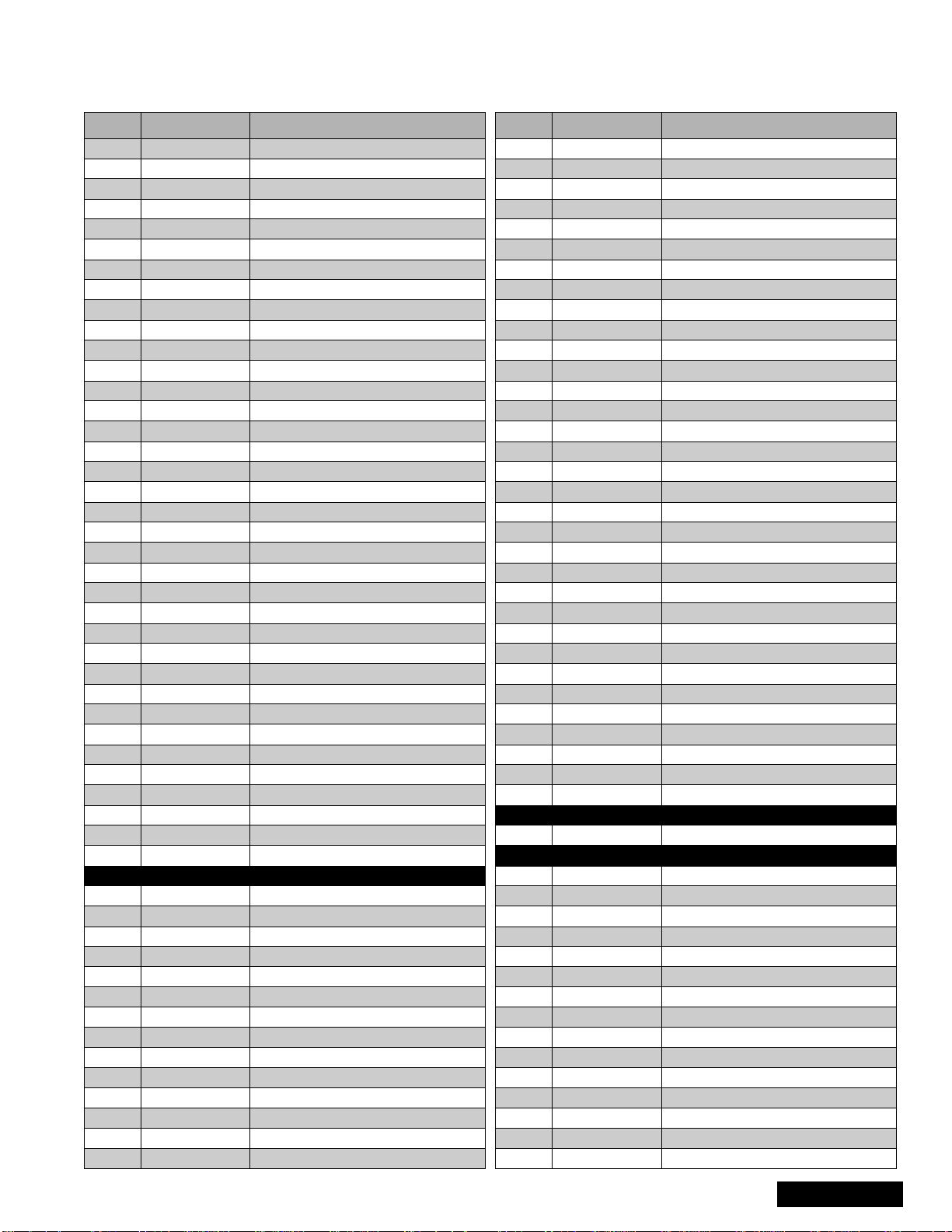
REPLACEMENT PARTS LIST
Models: CT-2022HBF, CT-2022HBCF.
Important Safety Notice: Components printed in BOLD TYPE have special c haracteristics important for safety. When replacing
any of these components use only manufacturer’s specified parts.
REF NO. PART NO. DESCRIPTION
C808 ECA1VM101B CAP,E 100UF-35V
C809 ECKR1H101KB5 CAP,C 100PF-K-50V
C810 ECKR1H471KB5 CAP,C 470PF-K-50V
C812 ECQU2A224MVA CAP,P .22UF-M-250VAC
C813 ECQU2A153MVA CAP,P .015UF-M-250VAC
C814 ECQU2A153MVA CAP,P .015UF-M-250VAC
C820 ECA1CM101B CAP,E 100UF/16V
C821 TCJ2VB1H103K CAP,C .01UF-K-50V
C822 ECKR3A221KBP CAP,C 220PF-K-1KV
C823 ECA1HM471B CA P,E 470UF-50V
C824 ECKR3A102KBP CAP,C 1000PF-K-1KV
C825 EEUMG2C221S CAP,E 220UF-160V
C826 ECKR3A471KBP CAP,C 470PF-K-1KV
C827 ECA1CM221B CAP,E 10UF-16V
C828 ECA160V33UE CAP,E 33UF/160V
C1001 ECA1CM471E CAP,E 470UF-16V
C1002 TACCX103T50V CAP,C .01UF/50V
C1003 ECA0JM101B CAP,E 100UF-6.3V
C1004 TACCX103T50V CAP,C .01UF/50V
C1005 TACCX103T50V CAP,C .01UF/50V
C2215 EEANA1E100B CAP,E 10UF-25V
C2311 ECA1VM102E CAP,E 1000UF-35V
C2312 ECEA1HN010UB CAP,E 1UF/50V
C2313 ECA1EM101B CAP,E 100UF-25V
C2314 ECA1CM100B CAP,E 10UF-16V
C2317 ECA1CM102B CAP,E 1000UF/16V
C2330 ECA1CM100B CAP,E 10UF-16V
C2350 ECA1HM4R7B CAP,E 4.7UF-50V
C2401 ECA1EM100B CAP,E 10UF-25V
C2402 ECA1EM100B CAP,E 10UF-25V
C2403 ECA1EM4R7B CAP,E4.7UF/25V
C2404 ECA1CM221B CAP,E 10UF-16V
C3001 ECA1HM0R1B CAP,E 0.1UF/50V
C3015 ECA1HM010B CAP,E 1UF-50V
C3121 ECA1CM470B CAP,E 47UF/16V
C3122 TCJ2VB1H103K CAP,C .01UF-K-50V
DIODES
D002 MA165TA5VT DIODE, SWITCHING
D006 MA4330HTA DIODE
D052 MA4068MTA DIODE, ZENER
D053 MA4056MTA DIODE
D055 MA4056MTA DIODE
D451 ERA15-01V3 DIODE, RECTIFIER
D452 MA4047MTA DIODE
D453 MA165TA5VT DIODE, SWITCHING
D454 MA165TA5VT DIODE, SWITCHING
D456 MA4047MTA DIODE
D502 MA4047MTA DIODE
D531 AS01V0 DIODE
D551 D1NL20UV70 DIODE
D554 AU02V0 DIODE
REF NO. PART NO. DESCRIPTION
D558 RS3FS DIODE
D559 BYD33G-113 DIODE
D561 AU02V0 DIODE
D571 MA165TA5VT DIODE, SWITCHING
D606 MA165TA5VT DI ODE, SWITCHING
D607 MA152KTX DIODE
D608 MA152KTX DIODE
D609 MA152KTX DIODE
D801 D3SBA60-4103 DIODE
D806 TAP2AA0001 PTC 5-OHM
D808 SARS01V1 DIODE
D809 AG01V0 DIODE
D810 AG01V0 DIODE
D811 AG01V0 DIODE
D812 MA4068MTA DIODE, ZENER
D820 MA165TA5VT DIODE, SWITCHING
D821 MA4047HTA DIODE
D822 RN1ZLF-B1 DIODE
D823 S3L60P154004 DIODE
D824 D1NL20UV70 DIODE
D1001 MA4068MTA DIODE, ZENER
D1002 MA4068MTA DIODE, ZENER
D1003 MA4068MTA DIODE, ZENER
D2350 MA4068MTA DIODE, ZENER
D2351 MA165TA5VT DIODE, SWITCHING
D2352 MA165TA5VT DIODE, SWITCHING
D2353 MA165TA5VT DIODE, SWITCHING
D2354 MA4091MTA DIODE
D3001 MA3110MTX DI ODE, ZENER
D3017 MA3110MTX DIODE, ZENER
D3018 MA3110MTX DI ODE, ZENER
D3019 MA3110MTX DIODE, ZENER
D3020 MA3110MTX DI ODE, ZENER
FUSES
F801 XBA2A00101 FUSE 6.3A 125V
INTEGRATED CIRCUITS
IC001 M65580MAPA01 MPU
IC002 TVR2AJ113S EEPROM
IC003 RPM7138H5 REMOTE SENSOR
IC005 PQ1R33 3.3V REGULATOR
IC006 MN1280R RESET
IC050 TC74HC4066AL HALFTONE
IC451 LA7837-TV V OUT
IC551 AN78M09LB 9V REGULATOR
IC552 AN78M05LB PLUS 5V AVR
IC553 AN78M05LB PLUS 5V AVR
IC801 STRG5623A VCO (POWER SUPPLY)
IC1001 TC4066BP CLONE/MATE MULTIPLEXER
IC2302 AN17800A AUDIO OUT AMP
IC2401 AN5285K SOUND AGC
IC3101 TC74HC4066AL A/V SWITCH
PARTS LIST
219-02
-15-
Parts List
Page 16
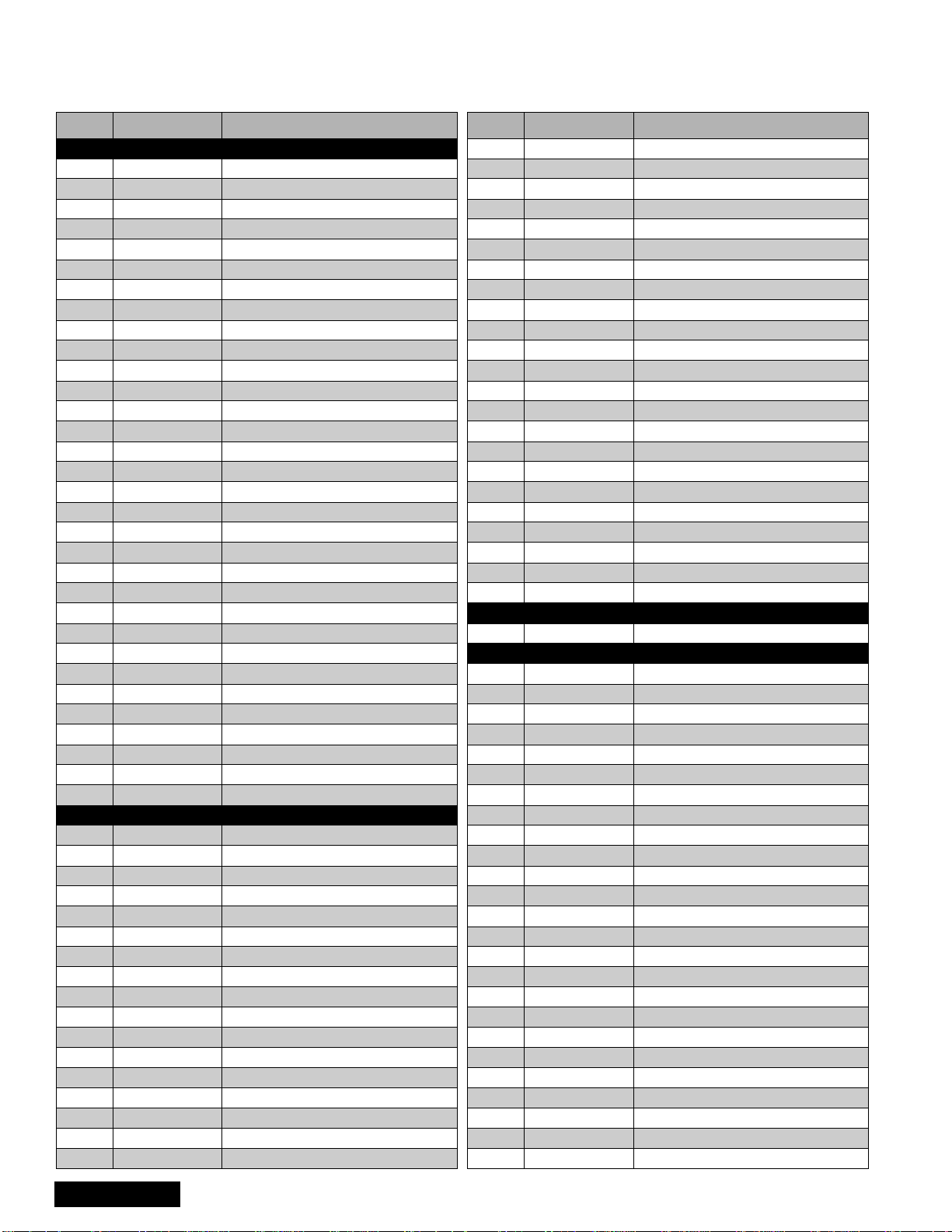
REPLACEMENT PARTS LIST
Models: CT-2022HBF, CT-2022HBCF.
Important Safety Notice: Components printed in BOLD TYPE have special c haracteristics important for safety. When replacing
any of these components use only manufacturer’s specified parts.
REF NO. PART NO. DESCRIPTION
COILS
L001 EXCELSA35T FERRITE BEAD
L003 TLUABTA2R2K COIL, PEAKING 2.2UH
L004 TLUABTA2R2K COIL, PEAKING 2.2UH
L005 EXCELDR35V FERRITEBEAD
L006 EXCELSA24T FERRITE BEAD
L007 EXCELDR35V FERRITEBEAD
L009 EXCELSA35V FERRITE BEAD
L010 ELESN330JA COIL, PEAKING 33UH
L011 ELESN330JA COIL, PEAKING 33UH
L013 EXCELDR35V FERRITEBEAD
L014 ELESN180KA COIL, PEAKING 18UH
L015 EXCELSA35V FERRITE BEAD
L016 EXCELSA35V FERRITE BEAD
L017 TLUABTA100K COIL, PEAKING 10UH
L018 TLUABTA150K COI L, PEAKING 15UH
L019 EXCELDR35V FERRITEBEAD
L090 EXCELSA24T FERRITE BEAD
L104 TLUABTA2R2K COIL, PEAKING 2.2UH
L108 EXCELSA35V FERRITE BEAD
L245 EXCELSA35V FERRITE BEAD
L250 EXCELSA35V FERRITE BEAD
L306 TLUABTA2R2K COIL, PEAKING 2.2UH
L325 EXCELSA35V FERRITE BEAD
L403 TLUABTA2R2K COIL, PEAKING 2.2UH
L416 EXCELSA39V FERRITE BEAD
L551 ELH5L4101 COIL
L801 ELF15N013A LINE FILTER
L802 ELEIE680KA COIL, PEAKING 68UH
L803 TA LL08T 680KA COI L
L2305 EXCELSA35V FERRITE BEAD
L2308 EX CELSA35V FERRITE BEAD
L2350 ELESN4R7JA COIL, PEAKING 4.7UH
TRANSISTORS
Q001 2SD601ARTX TRANSISTOR
Q006 2SB709ARTX TRA NSISTOR
Q007 2SB709ARTX TRANSISTOR
Q008 2SB709ARTX TRA NSISTOR
Q009 2SC1473A TRANSISTOR
Q050 2SB709ARTX TRA NSISTOR
Q051 2SB709ARTX TRANSISTOR
Q052 2SB709ARTX TRA NSISTOR
Q053 2SD601ARTX TRANSISTOR
PARTS LIST
Q054 2SD601ARTX TRANSISTOR
Q055 2SD601ARTX TRANSISTOR
Q090 2SB709ARTX TRA NSISTOR
Q092 2SB709ARTX TRANSISTOR
Q351 2SC3063RL TRANSISTOR
Q352 2SC3063RL TRANSISTOR
Q353 2SC3063RL TRANSISTOR
Q354 2SD601ARTX TRANSISTOR
REF NO. PART NO. DESCRIPTION
Q355 2SD601ARTX TRANSISTOR
Q356 2SD601ARTX TRANSISTOR
Q451 2SD601ARTX TRANSISTOR
Q452 2SD601ARTX TRANSISTOR
Q453 2SD601ARTX TRANSISTOR
Q501 2SC1573AH TRANSISTOR
Q505 2SD601ARTX TRANSISTOR
Q520 2SD601ARTX TRANSISTOR
Q551 2SD2499LBMA2 TRANSISTOR
Q605 2SB709ARTX TRANSISTOR
Q606 2SD601ARTX TRANSISTOR
Q820 2SA1767QTA TRANSISTOR
Q830 2SB1011QRL TRANSISTOR
Q1001 2SC1685QRSTA TRANSISTOR
Q1002 2SC1685QRSTA TRANSISTOR
Q1003 2SC1685QRSTA TRANSISTOR
Q1004 2SC1685QRSTA TRANSISTOR
Q1005 2SC1685QRSTA TRANSISTOR
Q1006 2SC1685QRSTA TRANSISTOR
Q1007 2SC1685QRSTA TRANSISTOR
Q2350 2SB709ARTX TRANSISTOR
Q3191 2SD601ARTX TRANSISTOR
Q3192 2SD601ARTX TRANSISTOR
RELAYS
RL801 TSEH0005 REL AY
RESISTORS
R001 ERJ6GEYJ102V RES,M 1K-J-1/10W
R003 ERJ6GEYJ105V RES,M 1M-J-1/10W
R004 ERJ6GEYJ562V RES,M 5.6K-J-1/10W
R006 ERDS2TJ101T RES,C 100-J-1/4W
R007 ERJ6GEYJ 471V RES,M 470-J-1/10W
R008 ERJ6GEYJ471V RES,M 470-J-1/10W
R009 ERJ6GEYJ472V RES,M 4.7K-J-1/10W
R010 ERJ6GEYJ682V RES,M 6.8K-J-1/10W
R011 ERJ6GEYJ682V RES,M 6.8K-J-1/10W
R012 ERJ6GEYJ473V RES,M 47K-J-1/10W
R013 ERJ6GEYJ202V RES,M 2K-J-1/10W
R014 ERJ6GEYJ221V RES,M 220-J-1/10W
R015 ERJ6GEYJ 221V RES,M 220-J-1/10W
R016 ERJ6GEYJ221V RES,M 220-J-1/10W
R017 ERJ6GEYJ 681V RES,M 680-J-1/10W
R018 ERJ6GEYJ681V RES,M 680-J-1/10W
R019 ERJ6GEYJ 681V RES,M 680-J-1/10W
R021 ERJ6GEYJ101V RES,M 100-J-1/10W
R022 ERJ6GEYJ 101V RES,M 100-J-1/10W
R023 ERJ6GEYJ102V RES,M 1K-J-1/10W
R024 ERJ6GEYJ 153V RES,M 15K-J-1/10W
R028 ERJ6GEYJ472V RES,M 4.7K-J-1/10W
R029 ERJ6GEYJ472V RES,M 4.7K-J-1/10W
R032 ERJ6ENF1002V RES,M 10K-F-1/10W
R033 ERJ6GEYJ222V RES,M 2.2K-J-1/10W
Parts List
-16-
219-02
Page 17
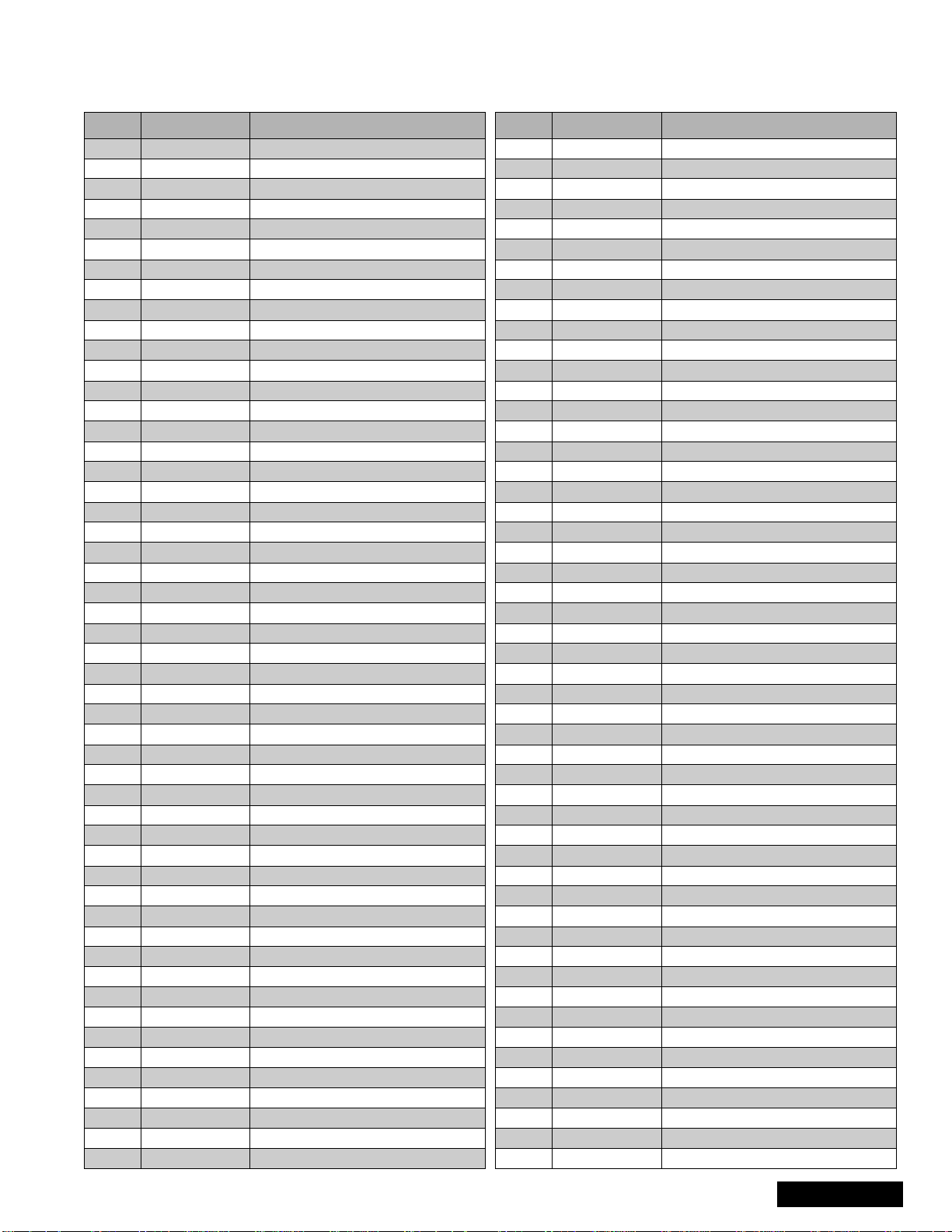
REPLACEMENT PARTS LIST
Models: CT-2022HBF, CT-2022HBCF.
Important Safety Notice: Components printed in BOLD TYPE have special c haracteristics important for safety. When replacing
any of these components use only manufacturer’s specified parts.
REF NO. PART NO. DESCRIPTION
R034 ERJ6GEYJ222V RE S,M 2.2K-J-1/10W
R035 ERJ6GEYJ332V RES,M 3.3K-J-1/10W
R036 ERJ6GEYJ562V RE S,M 5.6K-J-1/10W
R037 ERJ6GEYJ103V RES,M 10K-J-1/10W
R038 ERJ6GEYJ223V RE S,M 22K-J-1/10W
R039 ERJ6GEYJ 102V RES,M 1K-J-1/10W
R040 ERJ6GEYJ223V RE S,M 22K-J-1/10W
R041 ERJ6GEYJ153V RES,M 15K-J-1/10W
R042 ERJ6GEYJ392V RE S,M 3.9K-J-1/10W
R043 ERJ6GEYJ682V RES,M 6.8K-J-1/10W
R044 ERJ6GEYJ103V RE S,M 10K-J-1/10W
R045 ERJ6GEYJ101V RES,M 100-J-1/10W
R046 ERJ6GEYJ102V RE S,M 1K-J-1/10W
R062 ERJ6GEYJ 102V RES,M 1K-J-1/10W
R063 ERJ6GEYJ102V RE S,M 1K-J-1/10W
R064 ERJ6GEYJ 102V RES,M 1K-J-1/10W
R065 ERJ6GEYJ272V RE S,M 2.7K-J-1/10W
R066 ERJ6GEYJ272V RES,M 2.7K-J-1/10W
R067 ERJ6GEYJ272V RE S,M 2.7K-J-1/10W
R068 ERJ6GEYJ182V RES,M 1.8K-J-1/10W
R069 ERJ6GEYJ682V RE S,M 6.8K-J-1/10W
R070 ERJ6GEYJ 102V RES,M 1K-J-1/10W
R071 ERJ6GEYJ102V RE S,M 1K-J-1/10W
R072 ERJ6GEYJ 102V RES,M 1K-J-1/10W
R079 ERJ6GEYJ103V RE S,M 10K-J-1/10W
R081 ERJ6GEYJ103V RES,M 10K-J-1/10W
R090 ERJ6GEYJ471V RE S,M 470-J-1/10W
R091 ERJ6GEYJ185V RES, M 1.8MEG-J-1/10W
R092 ERJ6GEYJ473V RE S,M 47K-J-1/10W
R093 ERJ6GEYJ331V RES,M 330-J-1/10W
R201 ERJ6GEYJ472V RE S,M 4.7K-J-1/10W
R351 ERG2FJ123H RES,M 12K-J-2W
R352 ERG2FJ123H RES,M 12K-J-2W
R353 ERG2FJ123H RES,M 12K-J-2W
R354 ERDS1TJ272T RES,C 2.7K-J-1/2W
R355 ERDS1TJ272T RES,C 2.7K-J-1/2W
R356 ERDS1TJ272T RES,C 2.7K-J-1/2W
R357 ERJ6ENF4300V RES,M 430-F-1/10W
R358 ERJ6ENF4300V RES,M 430-F-1/10W
R359 ERJ6ENF4300V RES,M 430-F-1/10W
R360 ERJ6ENF7500V RES,M 750-F-1/10W
R361 ERJ6ENF7500V RES,M 750-F-1/10W
R362 ERJ6ENF7500V RES,M 750-F-1/10W
R363 ERJ6GEYJ101V RES,M 100-J-1/10W
R364 ERJ6GEYJ101V RE S,M 100-J-1/10W
R365 ERJ6GEYJ101V RES,M 100-J-1/10W
R370 ERDS2TJ224T RES,C 220K-J-1/4W
R381 ERJ6GEYJ101V RES,M 100-J-1/10W
R382 ERJ6GEYJ101V RE S,M 100-J-1/10W
R383 ERJ6GEYJ101V RES,M 100-J-1/10W
R384 ERJ6ENF2701V RES,M 2.7K-F-1/10W
REF NO. PART NO. DESCRIPTION
R385 ERJ6ENF7501V RES,M 7.5K-F-1/10W
R386 ERJ6ENF1201V RES,M 1.2K-F-1/10W
R387 ERJ6ENF2701V RES,M 2.7K-F-1/10W
R388 ERJ6ENF7501V RES,M 7.5K-F-1/10W
R389 ERJ6ENF1201V RES,M 1.2K-F-1/10W
R390 ERJ6ENF2701V RES,M 2.7K-F-1/10W
R391 ERJ6ENF7501V RES,M 7.5K-F-1/10W
R392 ERJ6ENF1201V RES,M 1.2K-F-1/10W
R450 ERJ6GEYJ 563V RES,M 56K-J-1/10W
R451 ERDS1FJ1R2P RES,C 1.2-J-1/2W
R454 ERJ6GEYJ 473V RES,M 47K-J-1/10W
R455 ERJ6GEYJ153V RES,M 15K-J-1/10W
R456 ERJ6GEYJ 562V RES,M 5.6K-J-1/10W
R457 ERJ6GEYJ162V RES,M 1.6K-J-1/10W
R458 ERJ6GEYJ 303V RES,M 30K-J-1/10W
R459 ERJ6GEYJ683V RES,M 68K-J-1/10W
R460 ERDS2TJ102T RE S, C 1K-J-1/4W
R462 ERJ6GEYJ473V RES,M 47K-J-1/10W
R463 ERJ6GEYJ 473V RES,M 47K-J-1/10W
R465 ERJ6GEYJ303V RES,M 30K-J-1/10W
R467 ERJ6GEYJ 183V RES,M 18K-J-1/10W
R468 ERJ6GEYJ103V RES,M 10K-J-1/10W
R469 ERJ6GEYJ 220V RES,M 22-J-1/10W
R471 ERJ6GEYJ223V RES,M 22K-J-1/10W
R472 ERJ6GEYJ 473V RES,M 47K-J-1/10W
R475 ERJ6GEYJ471V RES,M 470-J-1/10W
R502 ERJ6GEYJ 562V RES,M 5.6K-J-1/10W
R504 ERDS2TJ152T RES,C 1.5K-J-1/4W
R505 ERJ6GEYJ 222V RES,M 2.2K-J-1/10W
R506 ERJ6GEYJ333V RES,M 33K-J-1/10W
R507 ERJ6GEYJ 103V RES,M 10K-J-1/10W
R508 ERJ6GEYJ103V RES,M 10K-J-1/10W
R510 ERG3FJ182 RES,M 1.8K-J-3W
R512 ERG2FJ562H RES,M 5.6K-J-2W
R520 ERJ6GEYJ 471V RES,M 470-J-1/10W
R521 ERJ6GEYJ272V RES,M 2.7K-J-1/10W
R531 ERD25FJ470P RES,C 47-J-1/4W
R532 ERJ6ENF1372V RES, M 13.7K-F-1/10W
R533 ERJ6ENF1821V RES,M 1.82K-F-1/10W
R551 ERDS1FJ1R0T RES,C 1.0-J-1/2W
R552 ERDS1FJ1R0T RES,C 1.0-J-1/2W
R555 ERDS1FJ101T RES,C 100-J-1/2W
R556 ERG1SJ221P RES,M 220-J-1W
R557 ERJ6GEYJ103V RES,M 10K-J-1/10W
R558 ERQ2CJP3R0S RES,F 3.0-J-1/4W
R559 ERG2FJ683H RES,M 12K-J-2W
R562 ERG3FJ680H RES,M 68-J-3W
R563 ERG1SJ150P RES,M 15-J-1W
R567 ERG2FJ122H RES,M 12K-J-2W
R572 ERJ6GEYJ222V RES,M 2.2K-J-1/10W
R605 ERDS2TJ103T RE S,C 10K-J-1/4W
PARTS LIST
219-02
-17-
Parts List
Page 18
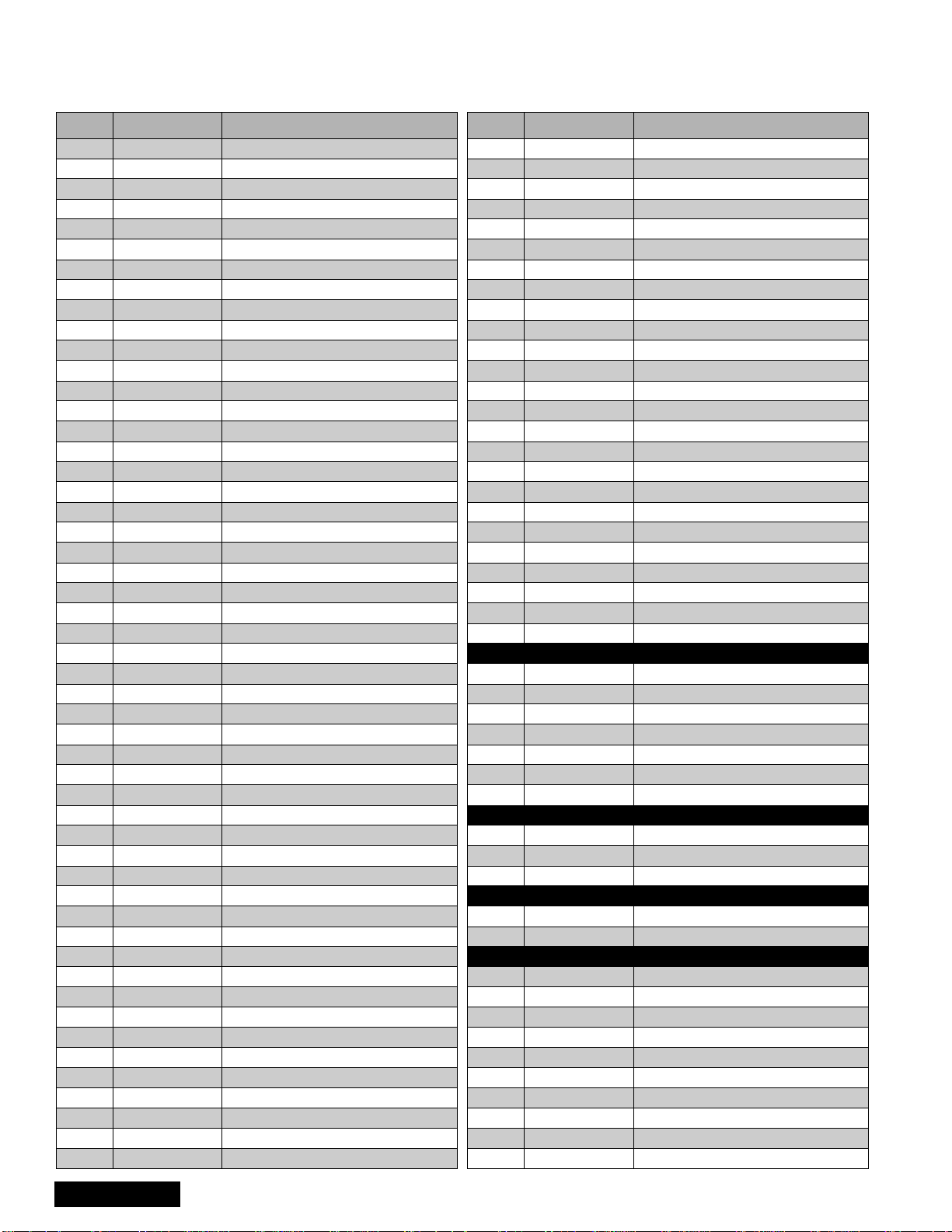
REPLACEMENT PARTS LIST
Models: CT-2022HBF, CT-2022HBCF.
Important Safety Notice: Components printed in BOLD TYPE have special c haracteristics important for safety. When replacing
any of these components use only manufacturer’s specified parts.
REF NO. PART NO. DESCRIPTION
R606 ERJ6GEYJ562V RE S,M 5.6K-J-1/10W
R607 ERJ6GEYJ 102V RES,M 1K-J-1/10W
R608 ERJ6GEYJ104V RE S,M 100K-J-1/10W
R801 ERF7ZK1R5 RES,W 1.5-K-7W
R802 ERDS2TJ684T RES,C 680K-J-1/4W
R803 ERG2FJ100H RES,M 10K-J-1/2W
R804 ERG2FJ104H RES,M 100K-J-2W
R805 ERX2FZJR18H RES,M .18-J-2W
R806 ERX2FJR56H RES,M .56-J-2W
R807 ERDS2TJ681T RES,C 680-J-1/4W
R808 ERDS2TJ4R7T RES,C 4.7-J-1/4W
R809 ERDS2TJ472T RES,C 4.7K-J-1/4
R815 ERC12ZGM825D RES,S 8.2MEG-M-1/2
R817 ERX3FJ6R8 RES,M 6.8-J-3W
R821 ERDS1FJ1R5T RES,C 1.5-J-1/2W
R822 ERDS1FJ1R5T RES,C 1.5-J-1/2W
R823 ERDS1FJ272T RES,C 2.7K-J-1/2W
R824 ERDS2TJ223T RES,C 22K-J-1/4W
R825 ERDS2TJ272T RES,C 2.7K-J-1/4W
R828 ERJ6GEYJ104V RES,M 100K-J-1/10W
R830 ERDS2TJ104T RES,C 100K-J-1/4W
R831 ERDS2TJ682T RES,C 6.8K-J-1/4W
R850 ERQ12HJR56P RES,F .56-J-1/2W
R1001 ERJ6GEYJ102V RES,M 1K-J-1/10W
R1002 ERJ6GEYJ101V RES,M 100-J-1/10W
R1003 ERJ6GEYJ101V RES,M 100-J-1/10W
R1004 ERJ6GEYJ102V RES,M 1K-J-1/10W
R1005 ERJ6GEYJ102V RES,M 1K-J-1/10W
R1006 ERJ6GEYJ102V RES,M 1K-J-1/10W
R1007 ERDS2TJ102T RES,C 1K-J-1/4W
R1008 ERJ6GEYJ102V RES,M 1K-J-1/10W
R1010 ERDS2TJ472T RES,C 4.7K-J-1/4
R1010 ERJ6GEYJ103V RES,M 10K-J-1/10W
R1011 ERDS2TJ103T RES,C 10K-J-1/4W
R1012 ERDS2TJ104T RES,C 100K-J-1/4W
R1013 ERDS2TJ103T RES,C 10K-J-1/4W
R1015 ERDS2TJ105T RES,C 1M-J-1/4W
R1017 ERDS2TJ681T RES,C 680-J-1/4W
R1018 ERDS2TJ101T RES,C 100-J-1/4W
R1019 ERDS2TJ101T RES,C 100-J-1/4W
R1020 ERDS2TJ561T RES,C 560-J-1/4W
R1021 ERDS2TJ103T RES,C 10K-J-1/4W
R1022 ERDS2TJ101T RES,C 100-J-1/4W
PARTS LIST
R1023 ERDS2TJ101T RES,C 100-J-1/4W
R1028 ERDS2TJ103T RES,C 10K-J-1/4W
R1029 ERDS2TJ103T RES,C 10K-J-1/4W
R1030 ERDS2TJ103T RES,C 10K-J-1/4W
R1031 ERDS2TJ103T RES,C 10K-J-1/4W
R1032 ERDS2TJ103T RES,C 10K-J-1/4W
R1033 ERDS2TJ104T RES,C 100K-J-1/4W
R1034 ERDS2TJ103T RES,C 10K-J-1/4W
REF NO. PART NO. DESCRIPTION
R1035 ERDS2TJ103T RES,C 10K-J-1/4W
R1036 ERDS2TJ102T RES,C 1K-J-1/4W
R1037 ERDS2TJ105T RES,C 1M-J-1/4W
R2301 ERQ2CJP3R9S RES,F 3.9-J-2W
R2307 ERJ6GEYJ103V RES,M 10K-J-1/10W
R2350 ERDS2TJ102T RES,C 1K-J-1/4W
R2351 ERJ6GEYJ273V RES,M 27K-J-1/10W
R2354 ERJ6GEYJ123V RES,M 12K-J-1/10W
R2355 ERJ6GEYJ392V RES,M 3.9K-J-1/10W
R2356 ERJ6GEYJ101V RES,M 100-J-1/10W
R2357 ERJ6GEYJ472V RES,M 4.7K-J-1/10W
R2365 ERDS2TJ102T RES,C 1K-J-1/4W
R2370 ERJ6GEYJ103V RES,M 10K-J-1/10W
R2401 ERJ6GEYJ225V RES,M 2.2M-J -1/10W
R2405 ERJ6GEYJ153V RES,M 15K-J-1/10W
R2406 ERJ6GEYJ243V RES,M 24K-J-1/10W
R3001 ERDS2TJ101T RES,C 100-J-1/4W
R3007 ERJ6GEYJ151V RES,M 150-J-1/10W
R3008 ERJ6GEYJ151V RES,M 150-J-1/10W
R3018 ERJ6GEYJ682V RES,M 6.8K-J- 1/10W
R3136 ERJ6GEYJ223V RES,M 22K-J-1/10W
R3137 ERJ6GEYJ223V RES,M 22K-J-1/10W
R3138 ERJ6GEYJ153V RES,M 15K-J-1/10W
R3139 ERJ6GEYJ333V RES,M 33K-J-1/10W
R3140 ERJ6GEYJ154V RES,M 150K-J-1/10W
SWITCHES
S001 EVQPF106K SWITCH
S002 EVQPF106K SWITCH
S003 EVQPF106K SWITCH
S004 EVQPF106K SWITCH
S005 EVQPF106K SWITCH
S008 EVQPF106K SWITCH
S009 EVQPF106K SWITCH
TRANSFORMERS
T501 ETH19Y211AZ TRANSFORMER
T551 KFT3AA341F TRANSFORMER, FLYBACK
T801 ETS29AS183NC TRANSFORMER
CRYSTALS/FILTERS
X001 TSSA092 CRYSTAL OSCILLATOR
X002 AF080005BE CRYSTAL
OTHERS
TNR001 ENG36604GR TUNER
M001 TSX2AA0212-2 A/C LINE C ORD
M002 A51JXS063X80 CRT
M003 TJSC00300 CRT SOCKET
M004 0FMK014ZZ CONVERGENCE CORRECTOR STRIP
M005 TMM2A30702 WEDGE, YOKE
DEG TSP2AA008A COIL, DEGAUSSING
M006 TXF3A011DB2 ASSY.DAG GROUND
M007 TXANV03ESER DEG.COIL INST. KIT
M008 TSN63115-4 MAGNET, PURITY
Parts List
-18-
219-02
Page 19
REPLACEMENT PARTS LIST
Models: CT-2022HBF, CT-2022HBCF.
Important Safety Notice: Components printed in BOLD TYPE have special c haracteristics important for safety. When replacing
any of these components use only manufacturer’s specified parts.
REF NO. PART NO. DESCRIPTION
ASSY, CABINET BACK
(Cabinet back, rubber sheet, overlay
model nameplate, 4 model nameplate,
M009 TXFKU22ESER
M010 TXFKY33ESER
M011 TAS2AA0012 SPEAKER 16-OHM 1.5W
M012 TBM2A10141 BADGE, PANASONIC
felt, instructions sheet labels, 3 label
X-ray warningfrench, label X-ray warning
spanish, label bbe patent, 3 label X-ray
warning)
ASSY, CABINET FRONT
(Cabinet front, badge PANASONIC,
smoked sheet, guide ir, label se rvice
information reference)
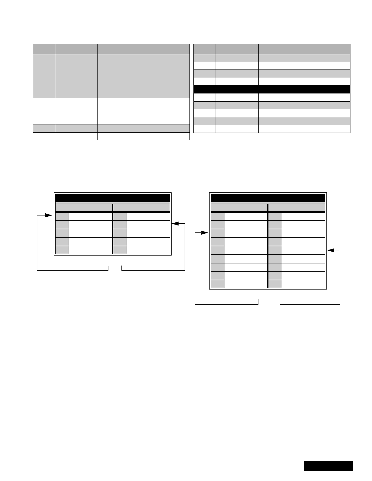
Description of abbreviations guide
RESISTOR
TYPE TOLERANCE
C Carbon F±1%
FFuseJ±5%
M Metal Oxide K ± 10%
SSolidM ± 20%
W Wire Wound G±2%
RES, C 270-J-1/4
REF NO. PART NO. DESCRIPTION
M013 TKX2A3753 GUIDE, IR
M014 TBX2AA00601G BUTTON, 7-KEY
JK1001 TJB2AX0021 MODULAR JACK
JK3002 TJB2AA0034 TERMINAL, FRONT A/V
ACCESSORIES
M015 EUR501450 REMOTE CONTROL
M016 UR50EC1190A BATTERYCOVER REMOTE CONTROL
M017 TQB2AA0387-2 MANUAL, OWNERS
M018 TQB2AA7057 REMOTE GUIDE
M019 TQB2AA7108 V-CHIP MANUAL
CAPACITOR
TYPE TOLERANCE
C Ceramic C ± 0.25pF
E Electrolytic D ± 0.5pF
P Polyester F ±1pF
SStyrolJ±5%
T Tantalum K ± 10%
L ± 15%
M ± 20%
P +10% -0%
Z +80% -20%
219-02
-19-
CAP, P .068UF-K-50V
PARTS LIST
Parts List
Page 20
Notes:
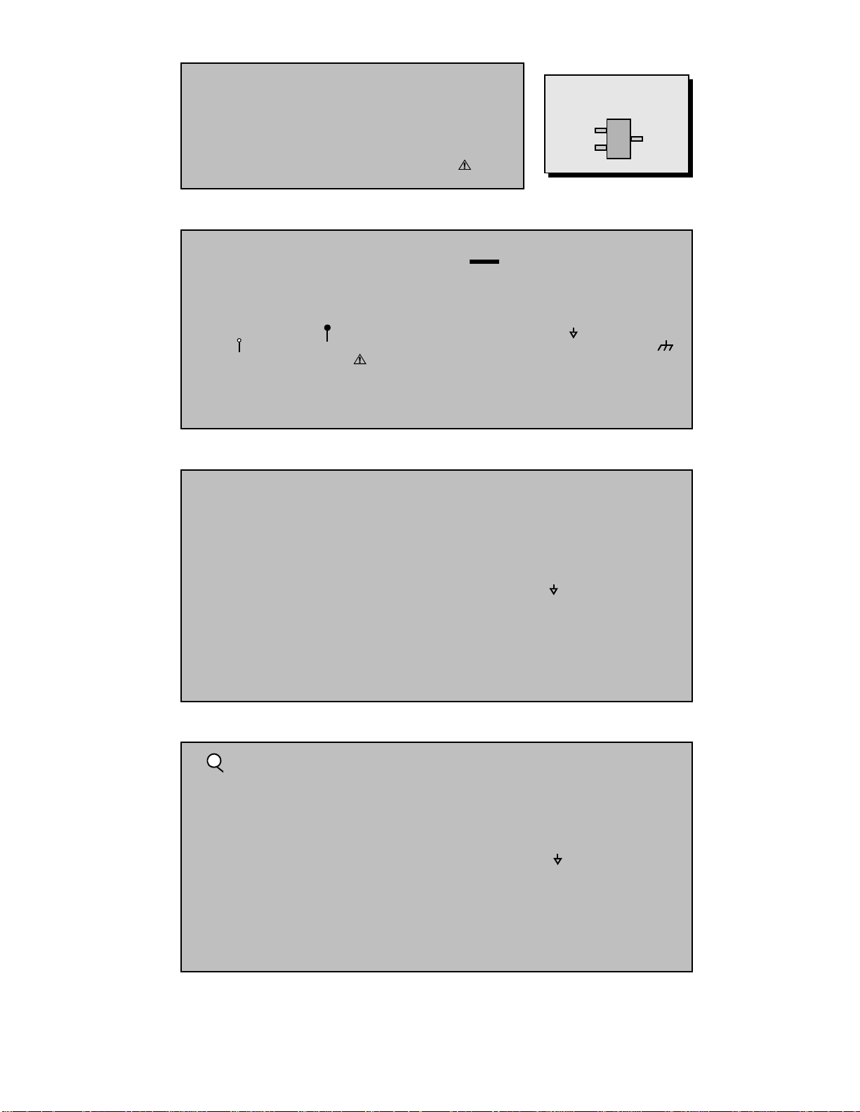
IMPORTANT SAFETY NOTICE
THIS S CHEMATIC DIAGRAM INCORPORATES SPECIAL
FEATURES THAT ARE IMPORTANT FOR PROTECTION FROM
X-RADIATION, FIRE AND ELECTRICAL SHOCK HAZARDS.
WHEN SERVICING IT IS ESSENTIAL THAT ONLY
MANUFACTURERS SPECIFIED PARTS BE USED FOR THE
CRITICAL COMPONENTS DESIGNATED WITH A IN THE
SCHEMATIC.
SCHEMATIC NOTES
1. Resistors are carbon 1/4W unless noted
otherwise.
2. Capacitors are ceramic 50V unless noted
otherwise.
3. Coil value notes is inductance in µH.
4. Test point indicated by ; Test point but no
pin .
5. Components indicated with are critical
parts and replacement should b e made
with manufacture specified replacement
parts only.
6. (BOLD LINE) indicates the route
of B+ supply.
7. The schematic diagrams are current at
the time of printing and are subject to
change without notice.
8. Ground symbol indicates HOT
GROUND CONNECTION;
indicates COLD GROUND.
NOTE: All other component symbols are
VOLTAGE MEASUREMENTS
1. Voltage measurement:
- AC input to t he Receiver is 120V.
NTSC (HD, 1125i & 525P when
applicable) signal generator is
connected to the antenna of the
Receiver. (Color bar pattern of 100
IRE white and 7.5 IRE black.)
- All Picture and Audio adjustments are
set to Normalize.
TV ANT/CABLE - (Set-Up Menu) in
TV/ANT Mode
Volume - Min.
TV/Video SW - TV position
Audio Mode - Stereo
- Voltage readings are nom inal and
may vary ±10% on active devices.
Some voltage reading will vary
with signal strength and picture
content.
- Supply voltages are nominal.
2. Ground symbol indicates ground lead
connection of meter.
Incorrect ground connection will result
in erroneous readings.
CAUTION: Incorrect ground connection
of the test equipment will result in
erroneous readings.
CHIP TRANSISTOR
LEAD DESIGNATION
B
E
used for engineering design
purposes.
C
3
1. indicates waveform measurement.
(Measurement can be taken at the best
accessible location in common to the
indicated point.)
2. Taken with an NTSC signal generator
connected to the antenna terminal.
(NTSC c olo r bar pattern of 8 bars of EIA
colors, 100 IRE white and 7.5 IRE black.)
3. Customer Controls (Picture/Audio Menu) are
set to Normalize. Volume is set to “MIN”.
WAVEFORM MEASUREMENTS
4. All video and color waveforms are taken
with a wideband scope and a probe
with low capacitance (10 to 1). Shape
and peak altitudes may vary
depending on the type of Oscilloscope
used and its settings.
5. Ground symbol shown on waveform
number indicates (Hot) ground lead
connection of the Oscilloscope.
CAUTION: Incorrect ground connection of
the test equipment will result in erroneous
readings.
PARTS LIST
-20-
Page 21
Notas
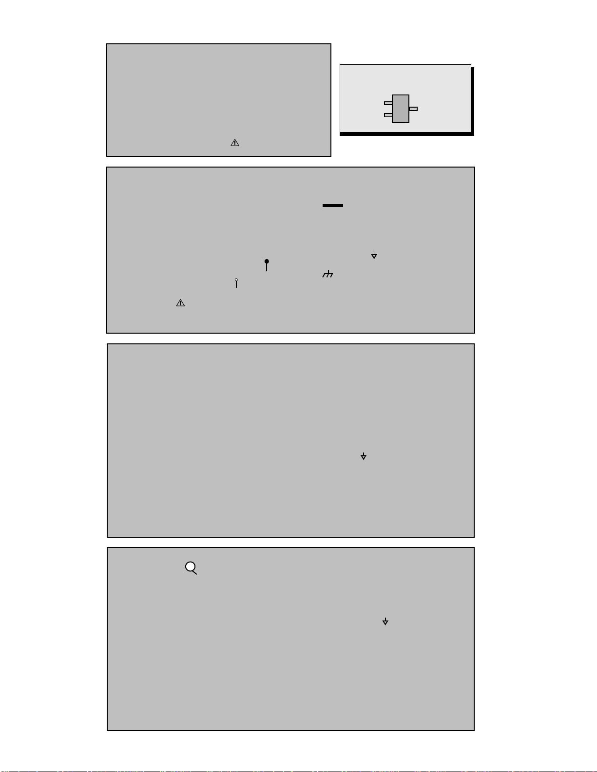
NOTA DE SEGURIDAD
LOS DIAGRAMAS ELÉCTRICOS INCLUYEN
CARACTERÍSTICAS ESPECIALES MUY IMPORTANTES
PARA LA PROTECCIÓN CONTRA RAYOS-X,
QUEMADURAS Y DESCARGAS ELÉCTRICAS. CUANDO
SE DE SERVICIO ES IMPORTANTE USAR PARA
REEMPLAZO DE COMPONENTES CRITICOS, SOLO
PARTES ESPECIFICADAS POR EL FABRICANTES. LOS
COMPONENTES CRITICOS ESTAN SEÑALADOS EN LOS
DIAGRAMAS POR EL SIMBOLO .
NOTAS DE LOS DIAGRAMAS
1. Las Resistencias son de Carbón de 1/4W, a
menos que se indique otra característica.
2. Los Capacitores son de Cerámica para
50V, a menos que se indique otra
característica.
3. El valor indicado de las Bobinas es la
inductancia expresada en µH.
4. Los puntos de prueba en la terminal de
algún componente son indicados por Los
puntos de prueba fuera de los
componentes se indican con .
5. Los componentes señalados con el
símbolo son considerados
componentes críticos y deben ser
6. (LINEA GRUESA) indica las
7. Los diagramas eléctricos están sujetos a
8. El símbolo indica que es una
NOTA: Los demas símbolos de
IDENTIFICACIÓNDE TERMINALES
PARATRANSISTORES EN
B
E
reemplazados sólo con las partes
especificadas por el fabricante.
líneas de alimentación de los Voltajes
B+.
cambio sin previo aviso.
conexión a Tierra Caliente y el símbolo
indica conexión a Tierra Fría.
componentes incluidos son
usados con fines de diseño.
CHIP
C
MEDICIÓN DE VOLTAJES
1. Medición de voltaje:
- El voltaje de entrada al Receptor es de
120V de Corriente Alterna. Un
generador de patrones con formato
NTSC se conecta a la entrada de la
antena. (Patrón de Barras de Colores
con 100 IREs para el Blanco y 7.5 IREs
para el Negro.)
- Los ajustes de los Menus Picture y
Audio se normalizan.
EnelMenúSet-Up,enlaopción
ANTENA, se selecciona el modo de
CABLE.
El nivel de Volumen se minimiza.
De los modos TV y Video, seleccionar el
modo TV.
Seleccionarmodo Estereo del Audio.
MEDICIÓN DE FORMAS DE ONDA
1. Un símbolo como indica el punto paramedir
una señal. (La medición puede hacerse en
el punto con m ayor accesibilidad, siempre
que sea común al indicado.)
2. Se midieron utilizando un generador con
formato NTSC conectado a la terminal de la
antena. (Patrón de 8 Barras de Colores
EAI, formato NTSC de 100 IREs para el
Blanco y 7.5 IREs para el Negro.)
3. Los ajustes de usuario de los Menus
PICTURE y AUDIO se normalizaron.
Posteriormente el nivel de volumen se
ajusta al mínimo.
4. Las formas de onda de Video y Color
fueron tomadas con un osciloscopio de
3
- Las mediciones de los voltajes son
nominales y pueden variar hasta
10% en componentes en
funcionamiento. Las lecturas de los
voltajes pueden variar por la
potencia de la señal y el contenido
de la im agen.
- Las fuentes de voltajes son
nominales.
2. El símbolo indica el tipo de tierra que
se utiliza en la conexión del medidor.
PRECAUCION: SI no se utiliza la
conexión a la tierra adecuada, se
obtendrán mediciones equivocadas y
podría dañar el equipo de medición.
banda alta y con un punta de prueba de
baja capacitancia (10 a 1). La form a y
amplitud de las ondas puede variar
según el tipo de osciloscopio que se
utilice y sus características.
5. El símbolo de tierra que aparece junto al
número de la forma de onda, indica que
se utiliza conexión a Tierra Caliente en
el extremo negativo de la punta de
prueba.
PRECAUCION: Si no se utiliza la conexión
a la tierra adecuada, se obtendrán
mediciones equivocadas y podría dañar el
equipo de medición.
-21-
Page 22
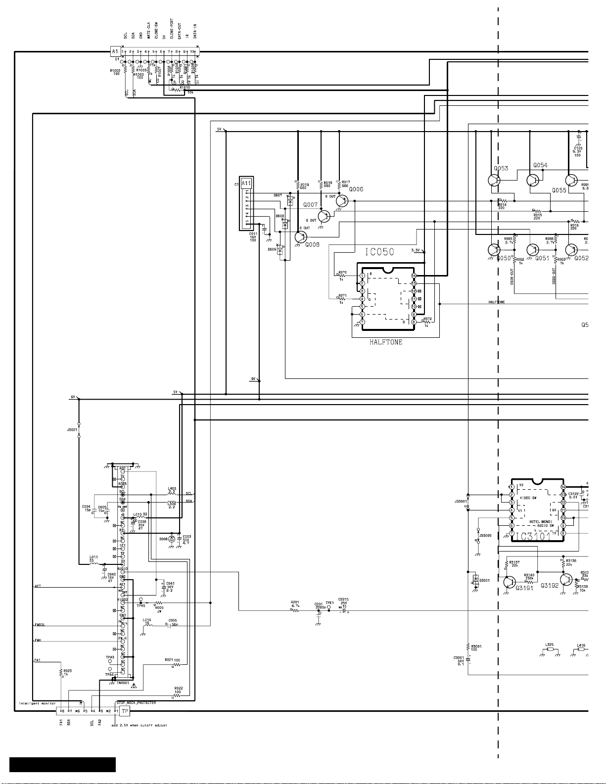
A-Board
- 22 -
Page 23
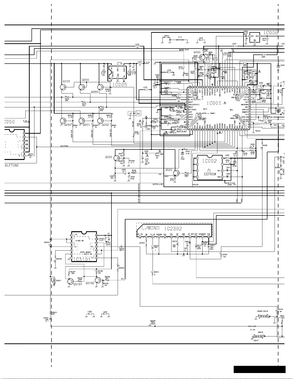
- 23 -
A-Board
Page 24
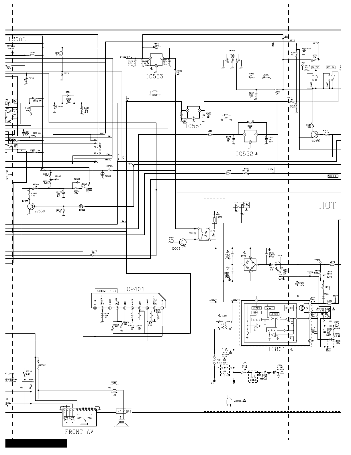
- 24 -A-Board
Page 25
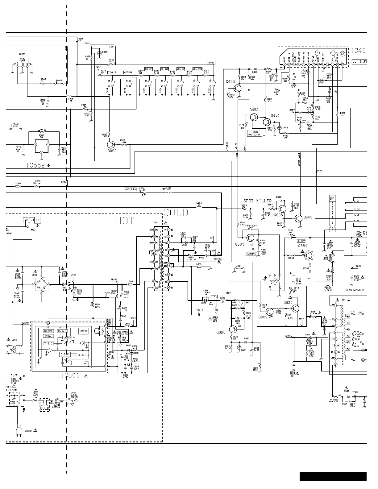
- 25 -
A-Board
Page 26
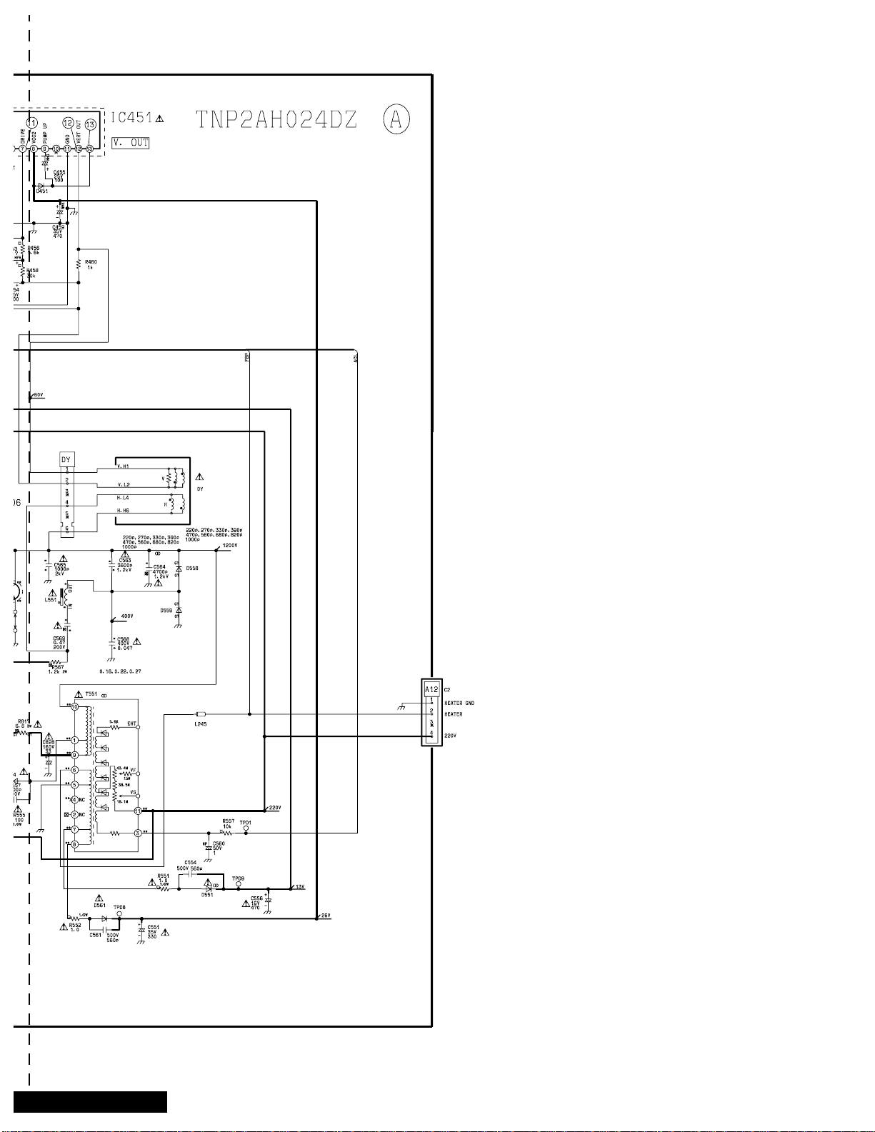
A-Board
- 26 -
Page 27
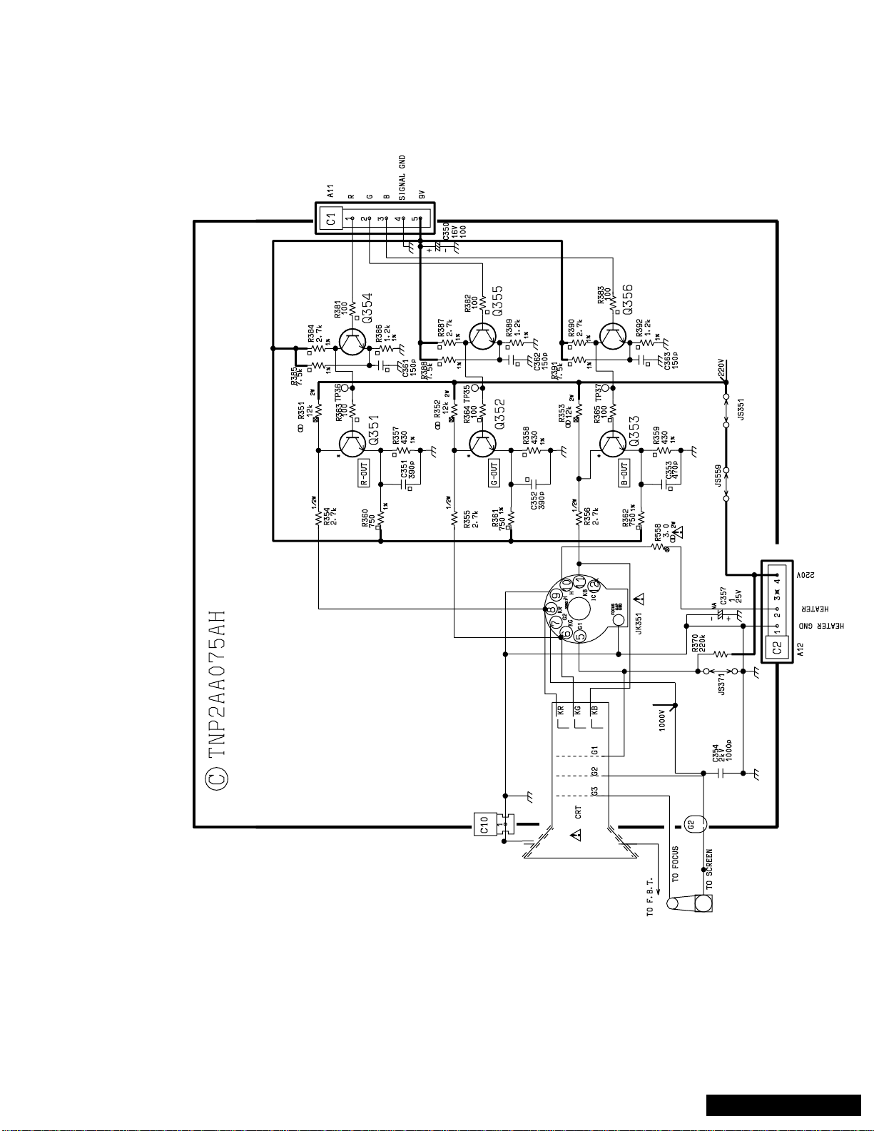
- 27 -
C-Board
Page 28

®
PrintedinUSA
K02082597PL0827
 Loading...