

Page 1
ACED020159C8
AUTOMOTIVE CONSUMER ELECTRONICS
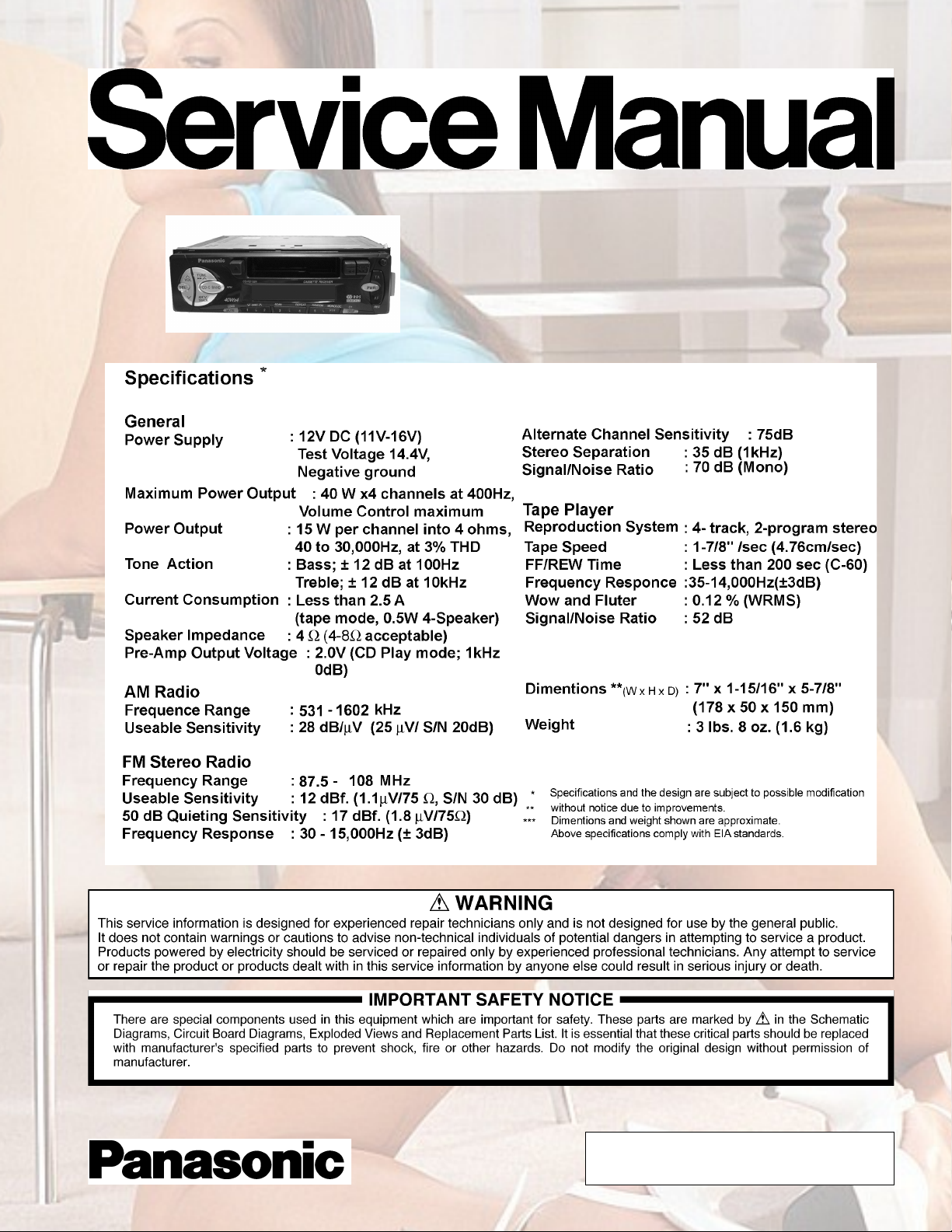
CQ-RD132N
Removable Face High-Power Cassette /
RDS Receiver with Changer Control
© 2002 Matsushita Electric Industrial Co., Ltd. All
rights reserved. Unauthorized copying and
distribution is a violation of law.
Page 2
CQ-RD132N
CONTENTS
Page Page
1 FEATURES 2
2 REPLACING THE FUSE
3 MAINTENANCE
4 RADIO ALIGNMENT
5 DIMENSIONS
6 WIRING CONNECTION
7 BLOCK DIAGRAM
8 TERMINALS DESCRIPTION
8.1. Main Block
8.2. Display Block
9 WIRING DIAGRAM
2
2
2
2
3
4
5
5
5
6
9.1. Main Block-1 6
9.2. Main Block-2
9.3. Display Block
10 SCHEMATIC DIAGRAM
10.1. Main Block
10.2. Display Block
11 PACKAGE AND IC BLOCK DIAGRAM
12 REPLACEM ENT PARTS LIST (Unit)
13 EXPLODED VIEW (Unit)
14 REPLACEM ENT PARTS LIST (Tape Player Parts)
15 EXPLODED VIEW (Tape Deck)
1 FEATURES
•
• PLL (Phase Locked Loop) Synthesized Tuning
• •
•
• 1DIN Size Body with Cassette Player,AM/FM Tuner, Power
• •
AMP (30Wx4)
•
• 18-FM , 6-AM stations preset
• •
•
• Auto preset and scan function
• •
•
• CD Changer Control function
• •
•
• Radio Data System(PS.AF.CT.P1)
• •
7
8
9
9
10
11
12
16
17
19
2 REPLACING THE FUSE
Be sure to use a fuse of the specified rating (10A) when
replacing a blown fuse. Fuses with higher capacity ratings,use
of any substitute, or connection without a fuse may result in a
fire hazard or damage to the unit.
3 MAINTENANCE
Your product is designed and manufactured to ensure a
minimum of maintenance. Use a soft cloth for routine exterior
cleaning. Never use benzine, or other solvent.
4 RADIO ALIGNMENT
Do not align the AM/FM package blocks. When the package
block is necessary, it will be supplied already aligned at the
factory.
5 DIMENSIONS
2
Page 3
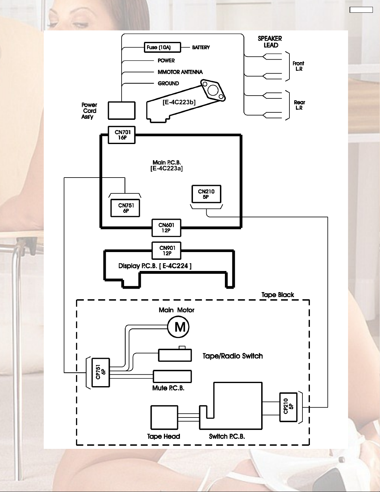
6 WIRING CONNECTION
CQ-RD132N
3
Page 4
CQ-RD132N
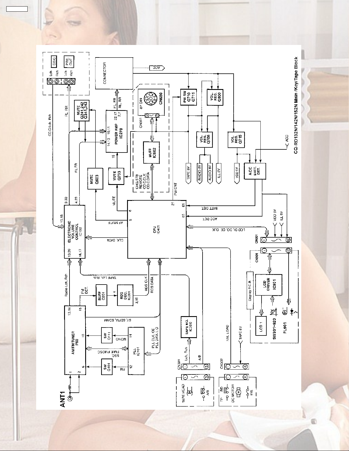
7 BLOCK DIAGRAM
4
Page 5
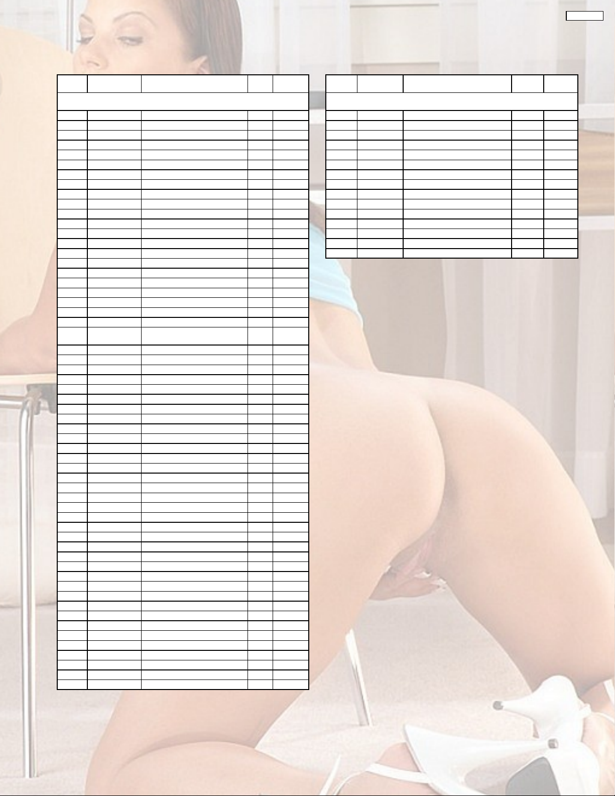
8 TERMINALS DESCRIPTION
CQ-RD132N
8.1. Main Block
Ref.
No.
IC401 YEAM7858459
1 INTC Specification setup I 4.8
2 SD FM B/S detection I 0.5
3 SD AM B/S detection I 0.5
4 AVSS Ground _ 0
5 AF MUTE AF mute output O 5
6 MUTE Mute output O 0
7 AVREF +5V power supply _ 5
8 LCD DATA I LCD data input I 4.7
9 LCD DATA O LCD data input O 0
10 LCD CLK LCD clock O 0
11 CD.C.DATA CD changer data I 0
12 NC No connection _ _
13 CD.C.CLK CD changer clock I 0
14 REMOTE CD changer remote cont. O 5
15 PLL CE PLL chip enable O 0
16 PLL DATA I PLL data I 5.2
17 PLL DATA O PLL data O 0
18 PLL CLK PLL clock O 5
19 LCD CE LCD chip enable O 0
20 NC No connection _ _
21 PW CNT System power control O 5
22~26 _ Not used _ _
27 F/R Tape forward/reverse
28 NC No connection _ _
29 ST FM stereo detection I 0
30~32 _ Not used _ _
33 VSS Ground _ 0
34 MOB Not used _ _
35 LED Security LED O 0
36 CLK Electronic volume clock O 5.3
37 DATA Electronic volume data O 5.3
38,39 NC No connection _ _
40 NC No connection _ _
41 NC No connection _ _
42 NC No connection _ _
43,44 _ Not used _ _
45 A/B Tape side detection I 5.1
46 T-IN Tape loading detection I 4.9
47~58 _ No connection _ _
59 RDS DATA RDS data input I 0
60 RESET Reset input I 4.6
61 BATT Battery level detection I 5.3
62 NC No connection _ _
63 RDS CLK RDS clock input I 2.6
64 CHG STB CD changer strobe I 0
65 ACC ACC leaver detection I 5
66 MOD (Connecting to ground) _ 0
67 NC (Connecting to ground) _ 0
68 VDD +5V power supply _ 5
69 X2 Crystal oscillator _ 2.3
70 X1 Crystal oscillator _ 1.7
71 VSS Ground _ 0
72 NC No connection _ _
73 VSS Ground _ 0
74~75 AVDD +5V power supply _ 5
76~78 _ (Connecting to ground) _ 0
79 INTA Specification setup I 0
80 INTB Specification setup I 4.8
Part No. Part Name & Description I/O Vol.(V)
detection
I 4.8
8.2. Display Block
Ref.
Part No. Description I/O Vol.(V)
No.
IC901 YEAMLC75854W
1~34 SEG1~34 LCD segment O 2.5
35~39 NC No connection _ _
40~43 COM1~4 LCD common O 2.5
44~49 KS1~6 Key data output O 0.9
50~54 K11~5 Key data input I 0.0
55 TEST (Connecting to ground) _ 0.0
56 VDD +5V power supply _ 5.1
57 VDD1 Ground through capacitor _ 3.3
58 VDD2 Ground through capacitor _ 1.7
59 Vss Ground _ 0.0
60 OSC CR oscillator _ 3.9
61 DO Key data output O 4.4
62 CE Chip enable I 0.0
63 CLK LCD clock I 0.0
64 D1 LCD data input I 0.0
5
Page 6
CQ-RD132N
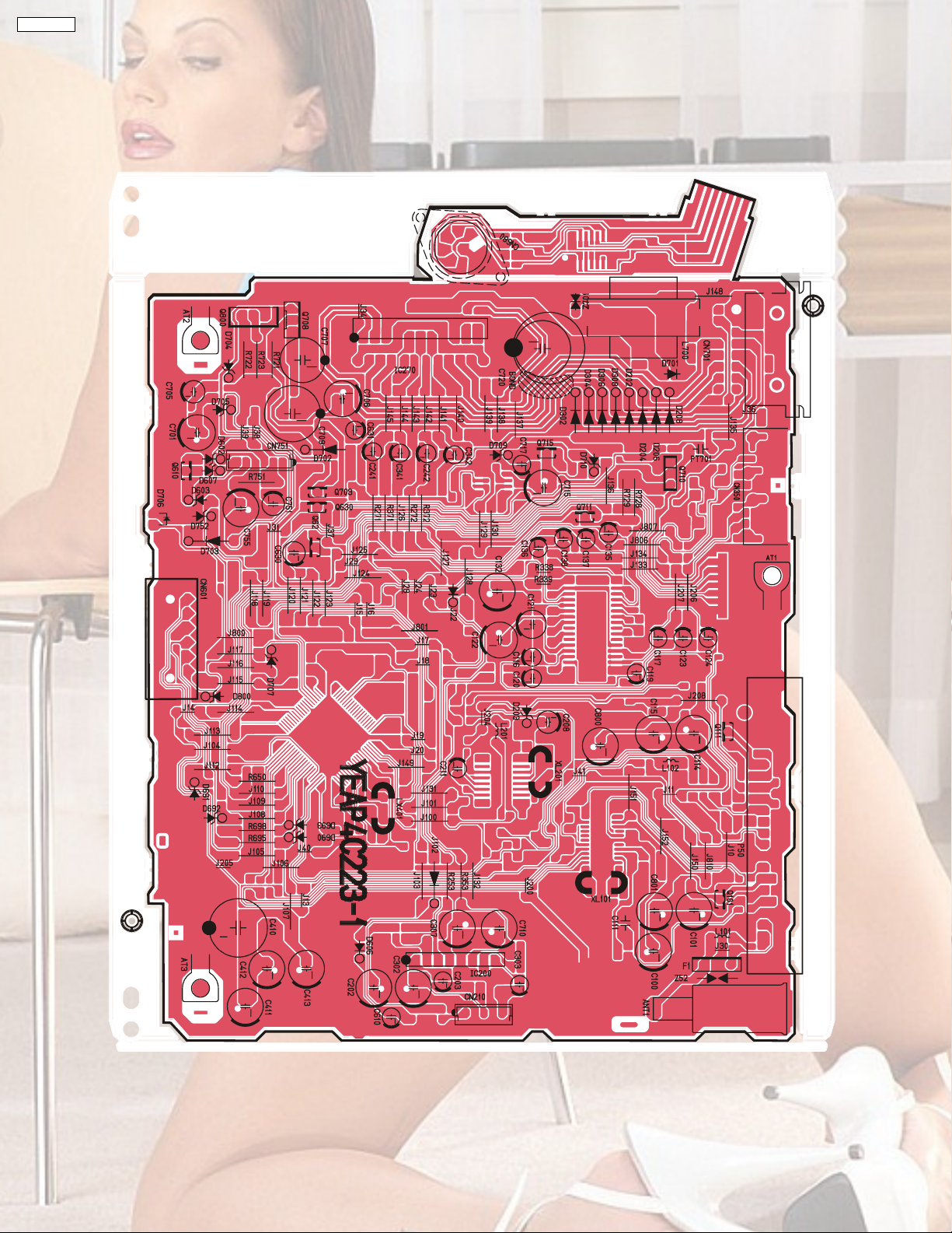
9 WIRING DIAGRAM
9.1. Main Block-1
[E-4C223][Top VIEW]
CQ-RD132N / 142N / 152N Main PCB
6
Page 7
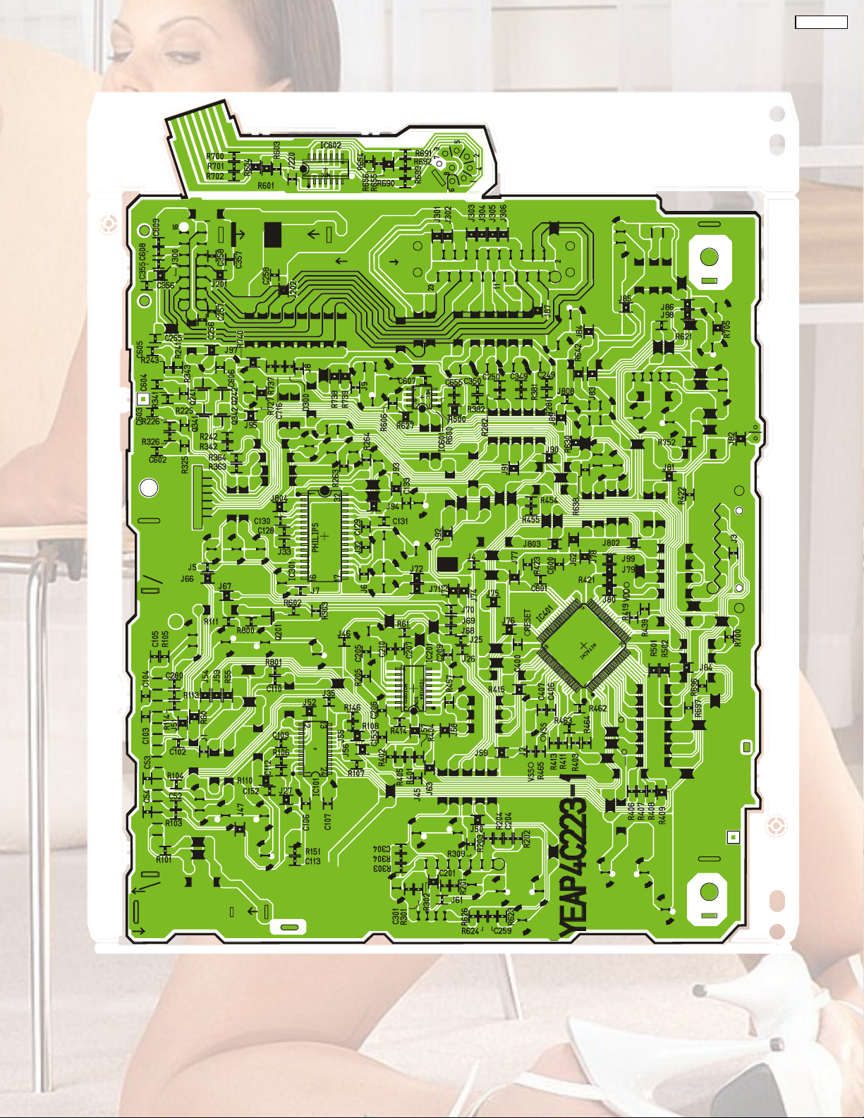
9.2. Main Block-2
CQ-RD132N
[E-4C223][Bottom VIEW]
CQ-RD132N / 142N / 152N Main PCB
7
Page 8

CQ-RD132N
9.3. Display Block
[E-4C224][Top VIEW]
CQ-RD132N / 142N / 152N Display PCB
[E-4C224][Bottom VIEW]
CQ-RD132N / 142N / 152N Display PCB
8
Page 9

10 SCHEMATIC DIAGRAM
10.1. Main Block
CQ-RD132N
E-4C223
CQ-RD132N / 142N / 152N Main Block
9
Page 10

CQ-RD132N
10.2. Display Block
E-4C224
10
CQ-RD132N / 142N / 152N Display Block
Page 11

11 PACKAGE AND IC BLOCK DIAGRAM
CQ-RD132N
11
Page 12

CQ-RD132N
12 REPLACEMENT PARTS LIST (Unit)
Ref.
No.
1. IC’s and Transistors
MAIN BLOCK [E-4C223]
IC101 YEAMLC72146T IC T
IC200 YEAMLA3161 IC T
IC201 YEAMDA7479D IC
IC270 YEAMTDA8571J IC
IC301 YEAMEA6320TT IC
IC401 YEAM780058459 IC T
IC601 AN8065S-E1 IC
IC602 YEAMTC4584FN IC T
P50 CT-L01 Tuner T
Q101 YEANA123YST Transistor T
Q111 YEANDTA144ST Transistor T
Q201 YEANC1623T1 Transistor T
Q241 YEANDTC323TK Transistor T
Q242 YEANDTC323TK Transistor T
Q341 YEANDTC323TK Transistor T
Q342 YEANDTC323TK Transistor T
Q610 YEANKRC107M Transistor T
Q62 YEANDTA144ST Transistor T
Q630 YEANDTA144ST Transistor T
Q703 YEANKRC107M Transistor T
Q708 YEANKTC3205 Transistor T
Q710 YEANB1243QRT Transistor T
Q711 YEANKRC107M Transistor T
Q715 YEAN2SD1020T Transistor T
Q800 YEAND1762EF Transistor T
DISPLAY BLOCK [E-4C224]
IC901 YEAMLC75854W IC T
2. Diodes
MAIN BLOCK [E-4C223]
D202 YEAD1N4005ST Slicon Diode T
D203 YEADRD51JS3T Zener Diode T
D204 YEAD1N4005ST Slicon Diode T
D206 YEAD1N4005ST Slicon Diode T
D208 YEAD1N4005ST Slicon Diode T
D302 YEAD1N4005ST Slicon Diode T
D304 YEAD1N4005ST Slicon Diode T
D306 YEAD1N4005ST Slicon Diode T
D308 YEAD1N4005ST Slicon Diode T
D602 YEADMTZ82BT Zener Diode T
D603 YEAD1N4148C Diode T
D606 YEAD1N4148C Diode T
D607 YEADRD56JS3T Zener Diode T
D690 YEADRD56JS3T Zener Diode T
D691 YEADRD56JS3T Zener Diode T
D692 YEADRD56JS3T Zener Diode T
D693 YEADRD56JS3T Zener Diode T
D701 YEAD1N5404FT Slicon Diode T
Part No. Part Name & Description Remarks
Ref.
No.
D702 YEAD1N4005ST Slicon Diode T
D703 YEAD1N4005ST Slicon Diode T
D704 YEADMTZJ10CT Zener Diode T
D705 YEADRD51JS3T Zener Diode T
D706 YEADSLB24VR3 L.E.D(RED) T
D707 MA723TA Diode
D709 YEADRD56JS3T Zener Diode T
D710 YEAD1N4148C Diode T
D752 YEADRD51JS3T Zener Diode T
D800 YEAD1N4148C Diode T
Z51 YEADYP201M Surge Protector T
Z701 ERZG07DK470T ZNR T
DISPLAY BLOCK [E-4C224]
D902 MA8056LMHTX Diode
D903 MA8056LMHTX Diode
D904 MA8056LMHTX Diode
D905 MA8056LMHTX Diode
D919 YEAD1721SYGC LED(Green) T
D921 YEAD1721SYGC LED(Green) T
D922 YEAD1721SYGC LED(Green) T
D923 YEAD1721SYGC LED(Green) T
D924 YEAD1721SYGC LED(Green) T
D925 YEAD1721SYGC LED(Green) T
D926 YEAD1721SYGC LED(Green) T
D927 YEAD1721SYGC LED(Green) T
D928 YEAD1721SYGC LED(Green) T
D929 YEAD1721SYGC LED(Green) T
D930 YEAD1721SYGC LED(Green) T
D931 YEAD1721SYGC LED(Green) T
D932 YEAD1721SYGC LED(Green) T
D933 YEAD1721SYGC LED(Green) T
D934 YEAD1721SYGC LED(Green) T
D935 YEAD1721SYGC LED(Green) T
D936 YEAD1721SYGC LED(Green) T
3. Capacitors
MAIN BLOCK [E-4C223]
C100 ECEA1CKS101I Electrolytic 100MFD 16WV
C101 ECEA1CKS470I Electrolytic 47MFD 16WV
C102 ECUV1H103KBN Ceramic 0.01MFD 50WV T
C103 ECUV1H333KBN Ceramic 0.033MFD 50WV T
C104 ECUV1H333KBN Ceramic 0.033MFD 50WV T
C105 ECUV1H102KBN Ceramic 0.001MFD 50WV T
C106 ECUV1H180JCN Ceramic 18PF 50WV T
C107 ECUV1H180JCN Ceramic 18PF 50WV T
C109 ECUV1H103KBN Ceramic 0.01MFD 50WV T
C110 ECUV1H101KBN Ceramic 100PF 50WV T
C111 ECQV1H224JL2 Polyester 0.22MFD 50WV
C112 ECUV1H223KBN Ceramic 0.022MFD 50WV T
C113 ECUV1H103KBN Ceramic 0.01MFD 50WV T
C114 ECEA1AKS221I Electrolytic 220MFD 10WV
C115 ECEA1AKS221I Electrolytic 220MFD 10WV
C116 ECEA1HKS3R3I Electrolytic 3.3MFD 50WV
C117 ECEA1CKS100I Electrolytic 10MFD 16WV
C119 ECEA1CKS100I Electrolytic 10MFD 16WV
C120 ECEA1CKS100I Electrolytic 10MFD 16WV
C121 ECEA1CKS470I Electrolytic 47MFD 16WV
C122 ECEA1CKS101I Electrolytic 100MFD 16WV
C123 ECEA1CKS100I Electrolytic 10MFD 16WV
C124 ECEA1HKS3R3I Electrolytic 3.3MFD 50WV
C128 ECUV1H333KBN Ceramic 0.033MFD 50WV T
C129 ECUV1H333KBN Ceramic 0.033MFD 50WV T
C130 ECUV1H562KBN Ceramic 0.0056MFD 50WV T
C131 ECUV1H562KBN Ceramic 0.0055MFD 50WV T
C132 ECEA1AKS221I Electrolytic 220MFD 10WV
C133 ECUV1H103KBN Ceramic 0.01MFD 50WV T
C135 ECEA1HKS3R3I Electrolytic 3.3MFD 50WV
C136 ECEA1HKS3R3I Electrolytic 3.3MFD 50WV
C137 ECEA1HKS3R3I Electrolytic 3.3MFD 50WV
C138 ECEA1HKS3R3I Electrolytic 3.3MFD 50WV
C152 ECUV1H103KBN Ceramic 0.01MFD 50WV T
Part No. Part Name & Description Remarks
12
Page 13

Ref.
No.
C153 ECUV1H473KBN Ceramic 0.047MFD 50WV T
C201 ECUV1H122KBN Ceramic 0.0012MFD 50WV T
C202 ECEA1CKS101I Electrolytic 100MFD 16WV
C203 ECEA1HKS010I Electrolytic 1MFD 50WV
C204 ECUV1H273KBN Ceramic 0.027MFD 50WV T
C205 ECUV1H270JCN Ceramic 27PF 50WV T
C206 ECUV1H270JCN Ceramic 27PF 50WV T
C207 ECUV1H103KBN Ceramic 0.01MFD 50WV T
C208 ECEA1AKS470I Electrolytic 47MFD 10WV
C209 ECUV1H271KBN Ceramic 270PF 50WV T
C210 ECUV1H104KBN Ceramic 0.1MFD 50WV T
C211 ECEA1CKS100I Electrolytic 10MFD 16WV
C241 ECEA1HKS010I Electrolytic 1MFD 50WV
C242 ECEA1HKS010I Electrolytic 1MFD 50WV
C249 ECUV1H222KBN Ceramic 0.0022MFD 50WV T
C250 ECUV1H222KBN Ceramic 0.0022MFD 50WV T
C259 ECUV1H103KBN Ceramic 0.01MFD 50WV T
C280 ECUV1H471KBN Ceramic 470PF 50WV T
C301 ECUV1H122KBN Ceramic 0.0012MFD 50WV T
C302 ECEA1CKS101I Electrolytic 100MFD 10WV
C303 ECEA1HKS010I Electrolytic 1MFD 50WV
C304 ECUV1H273KBN Ceramic 0.027MFD 50WV T
C307 ECEA1CKS101I Electrolytic 100MFD 16WV
C341 ECEA1HKS010I Electrolytic 1MFD 50WV
C342 ECEA1HKS010I Electrolytic 1MFD 50WV
C349 ECUV1H222KBN Ceramic 0.0022MFD 50WV T
C350 ECUV1H222KBN Ceramic 0.0022MFD 50WV T
C400 ECUV1H104KBN Ceramic 0.1MFD 50WV
C406 ECUV1H150JCN Ceramic 15PF 50WV T
C407 ECUV1H150JCN Ceramic 15PF 50WV T
C410 YEECFYH0H223 Electrolytic 22000MFD 6.3WV
C411 ECEA0JKS331I Electrolytic 330MFD 6.3WV
C412 ECEA0JKS331I Electrolytic 330MFD 6.3WV
C413 ECEA0JKS331I Electrolytic 330MFD 6.3WV
C52 ECUV1H103KBN Ceramic 0.01MFD 50WV T
C53 ECUV1H103KBN Ceramic 0.01MFD 50WV T
C54 ECUV1H103KBN Ceramic 0.01MFD 50WV T
C600 ECUV1H104KBN Ceramic 0.1MFD 50WV T
C601 ECUV1H103KBN Ceramic 0.01MFD 50WV T
C607 ECUV1H104KBN Ceramic 0.1MFD 50WV T
C607 ECUV1H104KBN Ceramic 0.1MFD 50WV T
C610 ECEA1CKS100I Electrolytic 10MFD 16WV
C630 ECEA1CKS470I Electrolytic 47MFD 16WV
C631 ECEA1CKS100I Electrolytic 10MFD 16WV
C655 ECUV1H224ZFN Ceramic 0.22MFD 50WV T
C701 ECEA1CKS101I Electrolytic 100MFD 16WV
C705 ECEA1CKS100I Electrolytic 100MFD 16WV
C707 ECEA1AKS221I Electrolytic 220MFD 10WV
C708 ECEA1AKS221I Electrolytic 220MFD 10WV
C709 ECEA1CU222C Electrolytic 2200MFD 16WV
C710 ECEA1AKS221I Electrolytic 220MFD 10WV
C715 ECEA1CKS101I Electrolytic 100MFD 16WV
C716 ECUV1H224ZFN Ceramic 0.22MFD 50WV T
C717 ECEA1CKS100I Electrolytic 10MFD 16WV
C720 ECEA1CU332C Electrolytic 3300MFD 16WV
C751 ECEA1CKS100I Electrolytic 10MFD 16WV
C755 ECEA1AKS221I Electrolytic 220MFD 10WV
C800 ECEA1AKS221I Electrolytic 220MFD 10WV
C801 ECEA1AKS221I Electrolytic 220MFD 10WV
DISPLAY BLOCK [E-4C224]
C901 ECUV1H104KBN Ceramic 0.1MFD 50WV T
C902 ECUV1H561KBN Ceramic560MFD 50WV T
C903 ECUV1H102KBN Ceramic 0.001MFD 50WV T
C904 ECUV1H104KBN Ceramic 0.1MFD 50WV T
4. Resistors
MAIN BLOCK [E-4C223]
J1 ERJ6GEY0R00 Chip 0 ohms 1/10W T
J102 YEAD1N4148C Diode T
J2 ERJ6GEY0R00 Chip 0 ohms 1/10W T
J22 YEAD1N4148C Diode T
J220 ERJ6GEY0R00 Chip 0 ohms 1/10W T
J27 ERJ8GX0R00V Chip 0 ohms 1/8W T
J3 ERJ6GEY0R00 Chip 0 ohms 1/10W T
Part No. Part Name & Description Remarks
Ref.
No.
J301 ERJ8GX0R00V Chip 0 ohms 1/8W T
J302 ERJ8GX0R00V Chip 0 ohms 1/8W T
J303 ERJ8GX0R00V Chip 0 ohms 1/8W T
J304 ERJ8GX0R00V Chip 0 ohms 1/8W T
J305 ERJ8GX0R00V Chip 0 ohms 1/8W T
J306 ERJ8GX0R00V Chip 0 ohms 1/8W T
J32 ERJ6GEY0R00 Chip 0 ohms 1/10W T
J33 ERJ6GEY0R00 Chip 0 ohms 1/10W T
J35 ERJ6GEY0R00 Chip 0 ohms 1/10W T
J4 ERJ6GEY0R00 Chip 0 ohms 1/10W T
J45 ERJ6GEY0R00 Chip 0 ohms 1/10W T
J46 ERJ6GEY0R00 Chip 0 ohms 1/10W T
J47 ERJ8GX0R00V Chip 0 ohms 1/8W T
J5 ERJ6GEY0R00 Chip 0 ohms 1/10W T
J50 ERJ8GX0R00V Chip 0 ohms 1/8W T
J51 ERJ8GX0R00V Chip 0 ohms 1/8W T
J52 ERJ8GX0R00V Chip 0 ohms 1/8W T
J53 ERJ8GX0R00V Chip 0 ohms 1/8W T
J54 ERJ8GX0R00V Chip 0 ohms 1/8W T
J55 ERJ8GX0R00V Chip 0 ohms 1/8W T
J56 ERJ8GX0R00V Chip 0 ohms 1/8W T
J57 ERJ8GX0R00V Chip 0 ohms 1/8W T
J58 ERJ8GX0R00V Chip 0 ohms 1/8W T
J59 ERJ8GX0R00V Chip 0 ohms 1/8W T
J6 ERJ6GEY0R00 Chip 0 ohms 1/10W T
J62 ERJ8GX0R00V Chip 0 ohms 1/8W T
J63 ERJ8GX0R00V Chip 0 ohms 1/8W T
J64 ERJ8GX0R00V Chip 0 ohms 1/8W T
J66 ERJ8GX0R00V Chip 0 ohms 1/8W T
J67 ERJ8GX0R00V Chip 0 ohms 1/8W T
J68 ERJ6GEY0R00 Chip 0 ohms 1/10W T
J69 ERJ6GEY0R00 Chip 0 ohms 1/10W T
J7 ERJ6GEY0R00 Chip 0 ohms 1/10W T
J70 ERJ6GEY0R00 Chip 0 ohms 1/10W T
J71 ERJ8GX0R00V Chip 0 ohms 1/8W T
J72 ERJ8GX0R00V Chip 0 ohms 1/8W T
J73 ERJ8GX0R00V Chip 0 ohms 1/8W T
J74 ERJ8GX0R00V Chip 0 ohms 1/8W T
J75 ERJ8GX0R00V Chip 0 ohms 1/8W T
J76 ERJ8GX0R00V Chip 0 ohms 1/8W T
J77 ERJ8GX0R00V Chip 0 ohms 1/8W T
J78 ERJ8GX0R00V Chip 0 ohms 1/8W T
J79 ERJ8GX0R00V Chip 0 ohms 1/8W T
J8 ERJ6GEY0R00 Chip 0 ohms 1/10W T
J80 ERJ8GX0R00V Chip 0 ohms 1/8W T
J808 ERJ6GEY0R00 Chip 0 ohms 1/10W T
J81 ERJ8GX0R00V Chip 0 ohms 1/8W T
J82 ERJ8GX0R00V Chip 0 ohms 1/8W T
J83 ERJ8GX0R00V Chip 0 ohms 1/8W T
J84 ERJ8GX0R00V Chip 0 ohms 1/8W T
J85 ERJ8GX0R00V Chip 0 ohms 1/8W T
J86 ERJ8GX0R00V Chip 0 ohms 1/8W T
J87 ERJ8GX0R00V Chip 0 ohms 1/8W T
J88 ERJ8GX0R00V Chip 0 ohms 1/8W T
J89 ERJ8GX0R00V Chip 0 ohms 1/8W T
J9 ERJ6GEY0R00 Chip 0 ohms 1/10W T
J90 ERJ8GX0R00V Chip 0 ohms 1/8W T
J91 ERJ8GX0R00V Chip 0 ohms 1/8W T
J92 ERJ8GX0R00V Chip 0 ohms 1/8W T
J93 ERJ8GX0R00V Chip 0 ohms 1/8W T
J94 ERJ8GX0R00V Chip 0 ohms 1/8W T
J95 ERJ8GX0R00V Chip 0 ohms 1/8W T
J97 ERJ8GX0R00V Chip 0 ohms 1/8W T
J98 ERJ8GX0R00V Chip 0 ohms 1/8W T
J99 ERJ8GX0R00V Chip 0 ohms 1/8W T
R101 ERJ6GEYJ5R6 Chip 5.6 ohms 1/10W T
R103 ERJ6GEYJ101 Chip 100 ohms 1/10W T
R104 ERJ6GEYJ681 Chip 680 ohms 1/10W T
R105 ERJ6GEYJ153 Chip 15k ohms 1/10W T
R106 ERJ6GEYJ152 Chip 1.5k ohms 1/10W T
R107 ERJ6GEYJ222 Chip 2.2k ohms 1/10W T
R108 ERJ6GEYJ473 Chip 47k ohms 1/10W T
R110 ERJ8GEYJ221V Chip 220 ohms 1/8W T
Part No. Part Name & Description Remarks
CQ-RD132N
13
Page 14

CQ-RD132N
Ref.
No.
R111 ERJ6GEYJ100 Chip 10 ohms 1/10W T
R113 ERJ6GEYJ103 Chip 10k ohms 1/10W T
R114 ERJ6GEYJ103 Chip 10k ohms 1/10W T
R146 ERJ6GEYJ223 Chip 22k ohms 1/10W T
R151 ERJ6GEYJ182 Chip 1.8k ohms 1/10W T
R201 ERJ6GEYJ333 Chip 33k ohms 1/10W T
R202 ERJ6GEYJ330 Chip 33 ohms 1/10W T
R203 ERJ6GEYJ472 Chip 4.7k ohms 1/10W T
R204 ERJ6GEYJ124 Chip 120k ohms 1/10W T
R205 ERJ6GEYJ225 Chip 2200k ohms 1/10W T
R225 ERJ6GEYJ822 Chip 8.2k ohms 1/10W T
R226 ERJ6GEYJ332 Chip 3.3k ohms 1/10W T
R241 ERJ6GEYJ103 Chip 10k ohms 1/10W T
R242 ERJ6GEYJ103 Chip 10k ohms 1/10W T
R243 ERJ6GEYJ471 Chip 470 ohms 1/10W T
R253 ERDS25TJ562T Carbon 5.6k ohms 1/4W T
R263 ERJ6GEYJ101 Chip 100 ohms 1/10W T
R264 ERJ6GEYJ101 Chip 100 ohms 1/10W T
R271 ERD25TJ101 Carbon 100 ohms 1/4W T
R272 ERD25TJ101 Carbon 100 ohms 1/4W T
R281 ERJ6GEYJ223 Chip 22k ohms 1/10W T
R282 ERJ6GEYJ223 Chip 22k ohms 1/10W T
R301 ERJ6GEYJ333 Chip 3.3k ohms 1/10W T
R302 ERJ6GEYJ330 Chip 33 ohms 1/10W T
R303 ERJ6GEYJ472 Chip 4.7k ohms 1/10W T
R304 ERJ6GEYJ124 Chip 120k ohms 1/10W T
R309 ERJ6GEYJ221 Chip 220 ohms 1/10W T
R325 ERJ6GEYJ822 Chip 8.2k ohms 1/10W T
R326 ERJ6GEYJ332 Chip 3.3k ohms 1/10W T
R338 ERDS2TJ102 Carbon 1k ohms 1/4W T
R339 ERDS2TJ333 Carbon 33k ohms 1/4W T
R341 ERJ6GEYJ103 Chip 10k ohms 1/10W T
R342 ERJ6GEYJ103 Chip 10k ohms 1/10W T
R343 ERJ6GEYJ471 Chip 470 ohms 1/10W T
R353 ERDS25TJ562 Carbon 5.6k ohms 1/4W T
R363 ERJ6GEYJ101 Chip 100 ohms 1/10W T
R364 ERJ6GEYJ101 Chip 100 ohms 1/10W T
R371 ERD25TJ101 Carbon 100 ohms 1/4W T
R372 ERD25TJ101 Carbon 100 ohms 1/4W T
R381 ERJ6GEYJ223 Chip 22k ohms 1/10W T
R382 ERJ6GEYJ223 Chip 22k ohms 1/10W T
R401 ERJ6GEYJ103 Chip 10k ohms 1/10W T
R402 ERJ6GEYJ103 Chip 10k ohms 1/10W T
R403 ERJ6GEYJ473 Chip 47k ohms 1/10W T
R404 ERJ6GEYJ104 Chip 100k ohms 1/10W T
R405 ERJ6GEYJ104 Chip 100k ohms 1/10W T
R406 ERJ6GEYJ102 Chip 1k ohms 1/10W T
R407 ERJ6GEYJ102 Chip 1k ohms 1/10W T
R408 ERJ6GEYJ102 Chip 1k ohms 1/10W T
R409 ERJ8GEYJ102 Chip 1k ohms 1/8W T
R411 ERJ6GEYJ473 Chip 47k ohms 1/10W T
R414 ERJ6GEYJ103 Chip 10k ohms 1/10W T
R415 ERJ8GEYJ473V Chip 47k ohms 1/8W T
R419 ERJ6GEYJ473 Chip 47k ohms 1/10W T
R421 ERJ8GEYJ473V Chip 47k ohms 1/8W T
R422 ERJ6GEYJ102 Chip 1k ohms 1/10W T
R423 ERJ6GEYJ473 Chip 47k ohms 1/10W T
R439 ERJ6GEYJ473 Chip 47k ohms 1/10W T
R454 ERJ6GEYJ103 Chip 10k ohms 1/10W T
R455 ERJ6GEYJ103 Chip 10k ohms 1/10W T
R457 ERJ6GEYJ103 Chip 10k ohms 1/10W T
R462 ERJ6GEY0R00 Chip 0 ohms 1/10W T
R465 ERJ6GEYJ472 Chip 4.7k ohms 1/10W T
R500 ERJ8GEYJ224V Chip 220k ohms 1/8W T
R501 ERJ8GEYJ473V Chip 47k ohms 1/8W T
R502 ERJ8GEYJ473V Chip 47k ohms 1/8W T
R55 ERJ8GEYJ102V Chip 1k ohms 1/8W T
R60 ERJ8GX0R00V Chip 0 ohms 1/8W T
R600 ERJ6GEYJ333 Chip 33k ohms 1/10W T
R602 ERJ6GEYJ334 Chip 330k ohms 1/10W T
R606 ERJ6GE0R00 Chip 0 ohms 1/10W T
R61 ERJ6GEYJ121 Chip 120 ohms 1/10W T
R621 ERJ6GEYJ183 Chip 18k ohms 1/10W T
Part No. Part Name & Description Remarks
Ref.
No.
R623 ERJ6GEYJ563 Chip 56k ohms 1/10W T
R624 ERJ6GEYJ473 Chip 47k ohms 1/10W T
R626 ERJ6GEYJ472 Chip 4.7k ohms 1/10W T
R627 ERJ8GEYJ102 Chip 1k ohms 1/8W T
R630 ERJ8GEYJ102V Chip 1k ohms 1/8W T
R638 ERJ6GEYJ472 Chip 4.7k ohms 1/10W T
R642 ERJ8GEYJ103V Chip 10k ohms 1/8W T
R650 ERD25TJ102 Carbon 1k ohms 1/8W T
R654 ERJ6GEYJ473 Chip 47k ohms 1/10W T
R655 ERJ8GEYJ473V Chip 47k ohms 1/8W T
R656 ERJ6GEYJ473 Chip 47k ohms 1/10W T
R690 ERJ6GEYJ102 Chip 1k ohms 1/10W T
R691 ERJ6GEYJ102 Chip 1k ohms 1/10W T
R692 ERJ6GEYJ102 Chip 1k ohms 1/10W T
R693 ERJ6GEYJ102 Chip 1k ohms 1/10W T
R695 ERD25TJ102 Carbon 1k ohms 1/4W T
R696 ERJ6GEYJ102 Chip 1k ohms 1/10W T
R697 ERJ6GEYJ102 Chip 1k ohms 1/10W T
R698 ERD25TJ102 Carbon 1k ohms 1/4W T
R700 ERJ6GEYJ102 Chip 1k ohms 1/10W T
R701 ERJ6GEYJ102 Chip 1k ohms 1/10W T
R702 ERJ6GEYJ102 Chip 1k ohms 1/10W T
R705 ERJ8GEYJ331V Chip 330 ohms 1/8W T
R721 ERD25FJ5R6 Carbon 5.6 ohms 1/4W T
R722 ERD25TJ221 Carbon 220 ohms 1/4W T
R723 ERD25FJ5R6 Carbon 5.6 ohms 1/4W T
R727 ERJ8GEYJ473V Chip 47k ohms 1/8W T
R728 ERD25TJ681 Carbon 680 ohms 1/4W T
R729 ERD25TJ681 Carbon 680 ohms 1/4W T
R737 ERJ6GEYJ273 Chip 27k ohms 1/10W T
R738 ERJ8GEYJ330V Chip 33 ohms 1/8W T
R739 ERJ8GEYJ562V Chip 5.6k ohms 1/8W T
R740 ERJ8GEYJ154V Chip 150k ohms 1/8W T
R751 ERD25FJ2R7 Carbon 2.7 ohms 1/4W T
R752 ERJ8GEYJ103V Chip 10k ohms 1/8W T
R800 ERJ6GEYJ102 Chip 1k ohms 1/10W T
R801 ERJ6GEYJ473 Chip 47k ohms 1/10W T
R802 ERJ8GX0R00V Chip 0 ohms 1/10W T
R803 ERJ8GX0R00V Chip 0 ohms 1/10W T
R804 ERJ8GX0R00V Chip 0 ohms 1/10W T
R903 ERJ6GEYJ222 Chip 2.2k ohms 1/10W T
DISPLAY BLOCK [E-4C224]
R902 ERJ6GEYJ563 Chip 56k ohms 1/10W T
R903 ERJ6GEYJ102 Chip 1k ohms 1/10W T
R904 ERJ6GEYJ102 Chip 1k ohms 1/10W T
R905 ERJ6GEYJ102 Chip 1k ohms 1/10W T
R908 ERJ6GEYJ122 Chip 1.2k ohms 1/10W T
R909 ERJ6GEYJ102 Chip 1k ohms 1/10W T
R910 ERJ6GEY0R00 Chip 0 ohms 1/10W T
R921 ERJ6GEYJ181 Chip 180 ohms 1/10W T
R922 ERJ6GEYJ181 Chip 180 ohms 1/10W T
R923 ERJ6GEYJ391 Chip 390 ohms 1/10W T
R924 ERJ6GEYJ391 Chip 390 ohms 1/10W T
R925 ERJ6GEYJ391 Chip 390 ohms 1/10W T
R926 ERJ6GEYJ391 Chip 390 ohms 1/10W T
R980 ERJ6GEYJ103 Chip 10k ohms 1/10W T
5. Connectors
TAPE BLOCK
CN210 YEAE11H4105A Connector T
CP751 YEAE61H4106 Connector T
MAIN BLOCK [E-4C223]
CN210 YEAE2011P05 Connector T
CN601 YEAE012475 Connector
CN680 YEAE4CDIN023 Socket T
CN701 YEAE4CCON018 Connector T
CN751 YEAE2011P06 Connector T
DISPLAY BLOCK [E-4C224]
CN901 YEAE012476 Connector
6. Electric Parts
SWITCHES
SW901 K0H1BA000083 Tack Swich
SW902 YEAS094C030 Tack Swich
SW903 K0H1BA000083 Tack Swich
Part No. Part Name & Description Remarks
14
Page 15

Ref.
No.
SW904 K0H1BA000083 Tack Swich
SW905 YEAS094C030 Tack Swich
SW906 YEAS094C030 Tack Swich
SW907 YEAS094C030 Tack Swich
SW908 EVQ22704 Tack Swich T
SW909 EVQ22704 Tack Swich T
SW910 EVQ22704 Tack Swich T
SW911 YEAS094C030 Tack Swich
SW912 YEAS094C030 Tack Swich
SW913 YEAS094C030 Tack Swich
SW914 EVQ22704 Tack Swich T
SW915 K0H1BA000083 Tack Swich
SW916 EVQ22704 Tack Swich T
SW917 EVQ22704 Tack Swich T
SW918 YEAS094C030 Tack Swich
CRYSTAL
XL101 YEXL4C720TT Crystal T
XL201 YEXL4C433TT Crystal T
XL401 YEXL4C419TT Crystal T
COILS
L101 YELT02C470KT Axial Coil T
L102 YELT02C101KT Axial Coil T
L201 YELT02C101KT Axial Coil T
L700 YETQ024C035 Choke Coil T
LCD
LCD901 YEXDCM4C092 LCD T
LAMPS
PL901 YEAL34C008 Lamp T
POSISTOR
PT701 YERT7AR4R7MT Posistor
7. Accessories
PRINTING
INSTALLATION PARTS
8. Mechanical Parts
MISCELLANEOUS
F1 XBB1F100NS5 FUSE 10A
ANT1 YAA104C700ZA Ant Jack T(2-C)
AT1 YAT034C009 Terminal T(2-C)
AT2 YAT034C009 Terminal T(2-B)
AT3 YAT034C009 Terminal T(2-C)
1 YFA074C043ZA Front Plate T(2-B)
2 YFF014C032XA Heat Sink T(2-B)
3 YFA094C087ZA Right Plate Ass’y T(2-C)
4 YFA084C034ZA Rear Plate T(2-C)
5 YFA054C033ZA Under Cover T(1-C)
6 YFA034C040ZA Upper Cover T(4-C)
8 FX0214C276ZA IC Bracket T(2-B)
9 FX0214C246YA DECK BRACKET T(3-C)
10 YFC024C529ZA ESC Holder T(1-B)
11 YGFE134389 Push Button T(1-B)
12 YGFX0052057 Spring (Push Button) T(1-B)
13 YGFC05545 TRIM PLATE T(1-B)
14 XTN2+8GFZ Screw T(1-B)
15 YFC024C528ZA Rear Cover T(1-B)
16 YFX184C015ZA LCD Holder T(1-B)
17 FX0014C062ZA Panel Light (LCD) T(1-A)
19 XTB3+6FFXS Screw T
20 XSB26+4FX Screw T(2-C)
22 YFV024C039ZA Light Divergent Sheet T(1-A)
23 YEJT034C019 SCREW(CUP TIGHT 3X2) T(2-B)
24 FX0214C245ZA LCD Bracket T(1-A)
25 YEJT034C001 Screw T(2-B)
26 YFE134C340ZA Button (DISP) T(1-A)
27 YFE134C375ZA Button (POWER) T(1-A)
Part No. Part Name & Description Remarks
YFM284C359CA Operating Instructions T
YFM074C134CA Warranty Card T
YFC054C052ZA Unit Case T
YAJ024C090ZA Power Cord Ass’y T
YFG044C002ZA Stay T
YEFX0214198A Mounting Collr T
ZZBISR221 Bis Kit T
(3-B)
(2-C)
Ref.
No.
28 FX0054C048ZA SPRING T(1-A)
29 YFE134C372ZA BUTTON(TA/AF) T(1-A)
30 YFE134C341ZA BUTTON(RELEASE) T(1-A)
31 YFX024C054ZB CAST COVER T(2-B)
32 YFE134C371ZA BUTTON(1-5/PTY) T(1-A)
33 YFE134C339ZA BUTTON(MUTE) T(1-A)
34 YFE134C373ZA BUTTON(CD.C/BAND) T(1-A)
35 YFE134C374ZA BUTTON(SEL) T(1-A)
36 YFV024C060ZA SHEET T(1-A)
37 YFJ014C055ZA BLUE INDICATOR T(1-A)
38 YFE134C352ZA BUTTON(VOL UP/DOWN) T(1-A)
39 FX0054C045ZA SPRING(CAST) T(2-B)
40 YFC024C558ZA ESC PRINTING(front) T(1-A)
41 YJT034C015CA STEP SCREW T(2-B)
42 YFE134C346ZA BUTTON (EJECT) T(1-A)
43 YFE134C345ZA BUTTON (REW) T(1-A)
44 YFE134C344ZA BUTTON (FF) T(1-A)
45 YEFX9991682A RELEASE HOOK T(1-B)
46 FX0054C049ZA SPRING(HOOK) T(2-B)
47 YEAE4CRCA004 CONNECTOR ( RCA ) T(2-C)
48 XTW3+10C SCREW T(2-C)
49 XSB3+6FXS SCREW T(2-C)
51 YFE134C351ZA BUTTON(TUNE/TRACK) T(1-A)
52 FX0054C028ZA SPRING T(1-A)
53 FX0464C013YA EJECT LEVER T(3-B)
54 YFE134C148ZA EJECT LEVER HOLDER T(3-B)
55 YFE134C149ZA LEVER HOLDER T(3-B)
56 YEJT034C007 SCREW T(3-B)
57 YFV024C059ZA SHEET T(1-A)
Part No. Part Name & Description Remarks
(1-B)
CQ-RD132N
15
Page 16

CQ-RD132N
13 EXPLODED VIEW (Unit)
16
Page 17

14 REPLACEMENT PARTS LIST (Tape Player Parts)
Ref.N0. Part No. Part Name & Description Remarks
51 CG36-04-13 Pinch Arm Spring (2-D)
52 CG36-09-01 E-Ring F1.5 (4-D)
53 CG36-01-22 Pinch Arm ( R ) (1-C)
54 CG36-04-12 Pinch Arm Spring ( R ) (1-B)
55 CG36-01-24 Reverse Lever (1-C)
56 CG36-09-03 E-Ring F2.0 (1-C)
57 CG36-01-06 Bracket (3-D)
58 CG36-01-07 Program Arm (3-D)
59 CG36-01-08 Changer Lever ( B ) (3-D)
60 CG36-03-28 Changer Lever ( A ) (3-D)
61 CG36-01-11 Lock Lever (2-A)
62 CG36-06-07 BlacK Wire 60mm (4-C)
Ref.N0. Part No. Part Name & Description Remarks
MISCELLANEOUS
Ref.N0. Part No. Part Name & Description Remarks
1 CG36-01-01 Main Chassis (2-C)
2 CG36-03-04 Pulley Gear Shaft (1-C)
3 CG36-03-02 Reverse Gear Shaft (2-C)
4 CG36-03-03 Idler Pulley (A) Shaft (2-C)
5 CG36-03-01 Pinch Roller Arm Shaft (2-C)
6 CG36-02-01 CM Bracket (2-C)
7 CG36-06-01 Metal (2-C)
8 CG36-04-18 Earth Spring (2-C)
9 CG36-06-10 Power Switch (2-C)
10 TH1.7*6 Screw (2-B)
11 CG36-01-13 Eject CAM (2-B)
12 CG36-01-12 Eject Lever (2-B)
T CG36-04-08 Eject CAM Lock Spring (2-B)
14 CG36-03-22 Eject Lever Spring (2-B)
15 CG36-03-22 Eject CAM Shaft (2-C)
16 CG36-01-19 FR Arm (A) (1-C)
17 CG36-02-14 FF Arm (1-C)
18 CG36-01-20 FR Arm (B) (1-C)
19 CG36-02-18 TU Gear Arm (2-D)
20 CG36-03-23 TU Gear Saft (2-D)
21 CG36-02-19 TU Gear (2-D)
22 CG36-01-04 FR Changing Arm (3-C)
23 CG36-03-14 FR Changing Arm Shaft (3-B)
24 CG36-04-17 Changing Arm Shaft (3-C)
25 CG36-01-02 Head Plate (3-B)
26 CG36-03-07 Head Plate Shaft (3-B)
27 CG36-03-05 Head Shaft (A) (3-C)
28 CG36-03-06 Head Shaft (B) (3-C)
29 CG36-02-16 Adjust Link (3-B)
30 CG36-02-17 Tape Guide (4-B)
31 IO-2027 Screw (4-C)
32 CG36-01-25 Adjuster Shim (4-C)
33 CG36-02-15 Adjuster Arm (4-B)
34 IH-2050S Screw (4-B)
35 AP-42265 Head (4-B)
36 CG36-06-08 Read Wire 60mm (4-C)
37 CG36-04-11 Adjuster Arm Spring (B) (4-B)
38 CG36-04-10 Adjuster Arm Spring (A) (4-C)
39 CG36-01-23 Spring Push Plate (4-B)
40 IH-2040 Screw (4-C)
41 CG36-03-28 FF Roller (4-B)
42 CG36-08-07 P.Washer 1.2*3.2*0.25 (4-B)
(2-B)
43 CG36-03-26 H.P Roller (B) (3-B)
44 CG36-03-27 H.P Roller (A) (3-B)
45 CG36-08-05 P.Washer (3-B)
46 CG36-09-04 E-Ring F2.5 (3-B)
(3-C)
47 CG36-04-07 Head Plate Spring (3-C)
48 CG36-01-21 Pinch Arm (F) (2-D)
49 CG36-03-01 Pinch Arm Shaft (2-D)
50 CG36-05-03 Pinch Roller (2-D)
(1-C)
63 CG36-04-03 Lock Lever Spring (3-D)
64 CG36-03-17 Lock Lever Shaft (3-D)
65 CG36-03-21 FR Arm (A) Shaft (1-C)
66 CG36-03-20 Program Arm Shaft (3-D)
67 CG36-03-24 Program Arm Coller (3-D)
68 CG36-03-15 Changer Lever (A) Shaft (3-D)
69 CG36-06-09 White Wire 55mm (4-C)
70 CG36-04-09 Program Arm Spring (3-D)
71 CG36-03-19 Changer Lever (B) Shaft (3-D)
72 IF-2040 Screw (3-D)
73 CG36-06-11 Slide Switch P02-01 (2-D)
74 CG36-06-06 P.C.Plate (2-D)
75 CG36-08-04 Poly Washer 2.1*3.2*0.13 (1-D)
76 CG36-01-10 REW Lever (4-D)
77 CG36-01-09 FF Lever (4-D)
78 CG36-04-02 FF/REW Lever Spring (4-D)
79 CG36-09-03 E-Ring F2.0 (4-D)
80 CG36-02-22 Idler Pulley (A) (2-C)
81 CG36-02-02 Reel Base (2-A)
82 TP2050L Screw (1-C)
83 CG36-02-08 Pulley Gear (1-C)
84 CG36-01-03 Reel Plate (1-A)
85 CG36-03-08 Reel Shaft (1-A)
86 CG36-03-13 Sensor Arm Shaft (1-B)
87 CG36-03-10 Selecter Gear Shaft (1-A)
88 CG36-03-12 Gear Lock Arm Shaft (1-A)
89 CG36-03-11 Detector Gear Shaft (1-A)
90 CG36-03-09 Reduction Gear Shaft (1-A)
91 CG36-02-10 Detector Gear (1-A)
92 CG36-08-05 P.Washer 1.6*3*0.25 (1-A)
93 CG36-04-15 Dash Spring (1-A)
94 CG36-02-09 Selecter Gear (1-A)
95 CG36-03-29 Coller (1-A)
96 CG36-09-03 E-Ring F2.0 (1-A)
97 CG36-02-12 Sensor Arm (1-B)
98 CG36-02-05 Idler Gear(C) (2-B)
99 CG36-08-03 P.Washer 2.1*8*0.1 (2-A)
100 CG36-02-07 Reduction Gear (A) (2-B)
101 CG36-02-06 Reduction Gear (B) (2-A)
102 CG36-02-13 Gear Lock Arm (2-A)
103 CG36-04-04 Gear Lock Arm Spring (2-A)
104 CG36-02-11 Ratchet (2-A)
105 CG36-04-14 Ratchet Spring (2-A)
106 CG36-04-19 Back Tention Spring (2-A)
107 CG36-02-20 Detector (2-A)
108 CG36-02-03 Reel Gear (2-A)
109 CG36-02-04 Reel Cap (2-A)
110 CG36-04-10 Reel Clutch Spring (2-A)
111 CG36-08-05 P Washer 1.6*3*0.25C (2-A)
112 CG36-08-01 Reel Spacer (A) (2-A)
CQ-RD132N
(3-D)
(3-B)
(3-B)
(3-B)
(3-B)
(3-B)
(3-B)
(3-B)
(3-B)
17
Page 18

CQ-RD132N
Ref.N0. Part No. Part Name & Description Remarks
113 CG36-08-02 Reel Spacer (B) (2-A)
114 TP-2030 TP-2030 (2-B)
115 MCK-5U3LCKSNZ Motor (4-B)
116 CG36-03-25 Motor PullEY (3-B)
117 IO-2050 Screw (3-B)
118 CG36-05-02 Sub Belt (1-C)
119 CG36-06-13 Flywheel (F) (1-D)
120 CG36-06-14 Flywheel (R) (1-D)
121 CG36-03-33 Flywheel Shaft (1-D)
122 CG36-05-01 Main Belt 120.3*1*1 (1-D)
123 CG36-03-32 Flywheel Shaft (1-D)
124 CG36-08-04 P.Washer (2-C)
125 CG36-09-02 E-Ring F1.6 (3-C)
126 CG36-04-20 Selecter Link (3-C)
127 CG36-03-18 FF/REW Shaft (3-D)
128 IF-2040 Screw (2-D)
129 CG36-01-14 Cassette Hanger (4-A)
130 CG36-01-15 Cassette Holder (3-A)
131 CG36-01-16 Eject Cam Lock (3-A)
132 CG36-01-17 Center Plate (4-A)
133 CG36-04-21 Return Link (4-A)
134 CG36-04-16 Center Plate Spring (4-A)
135 CG36-04-08 Eject CAM Lock Spring (4-A)
136 CG36-02-21 Tape Hooker (4-A)
137 CG36-03-16 Eject CAM Lock Shaft (3-A)
138 CG36-06-05 Cushion 5*9.5*0.3 (3-A)
139 CG36-09-03 E-Ring F2.0 (4-A)
140 CG36-01-18 Lock Arm (1-A)
141 CG36-03-30 SW Arm Coller (1-A)
142 TH-1760 Screw (1-A)
143 CG36-06-12 Leaf Switch P01-15C (2-D)
144 CG36-06-03 Felt 14*6*0.8 (2-A)
145 1-0036-787-01 Leaf SW LSA-1112M1 (2-C)
146 1-0038-730-01 Mute PCB (2-C)
147 Z-1363-040-52 Screw M2*4 (2-C)
148 1-0036-234-01 Mute SW Arm (2-D)
149 1-0036-410-01 Mute Arm SPG (3-D)
150 1-0036-315-01 Mute SW Arm Coller (3-D)
151 TH-1740 Screw 1.7*4 (3-D)
(3-B)
(3-B)
(1-A)
(3-B)
18
Page 19

15 EXPLODED VIEW (Tape Deck)
CQ-RD132N
19
Printed in Taiwan
2002.01
Page 20

10 SCHEMATIC DIAGRAM
10.1. Main Block
E-4C223
9
Page 21

CQ-RD132N
CQ-RD132N / 142N / 152N Main Block
9
Page 22

CQ-RD132N
10.2. Display Block
10
Page 23

E-4C224
10
CQ-RD132N / 142N / 152N Display Block
 Loading...