

Panasonic CQJH-8062-Z, CQJH-8061-Z Service manual
ORDER No.0163
AUTOMOTIVE ELECTRONICS
HONDA
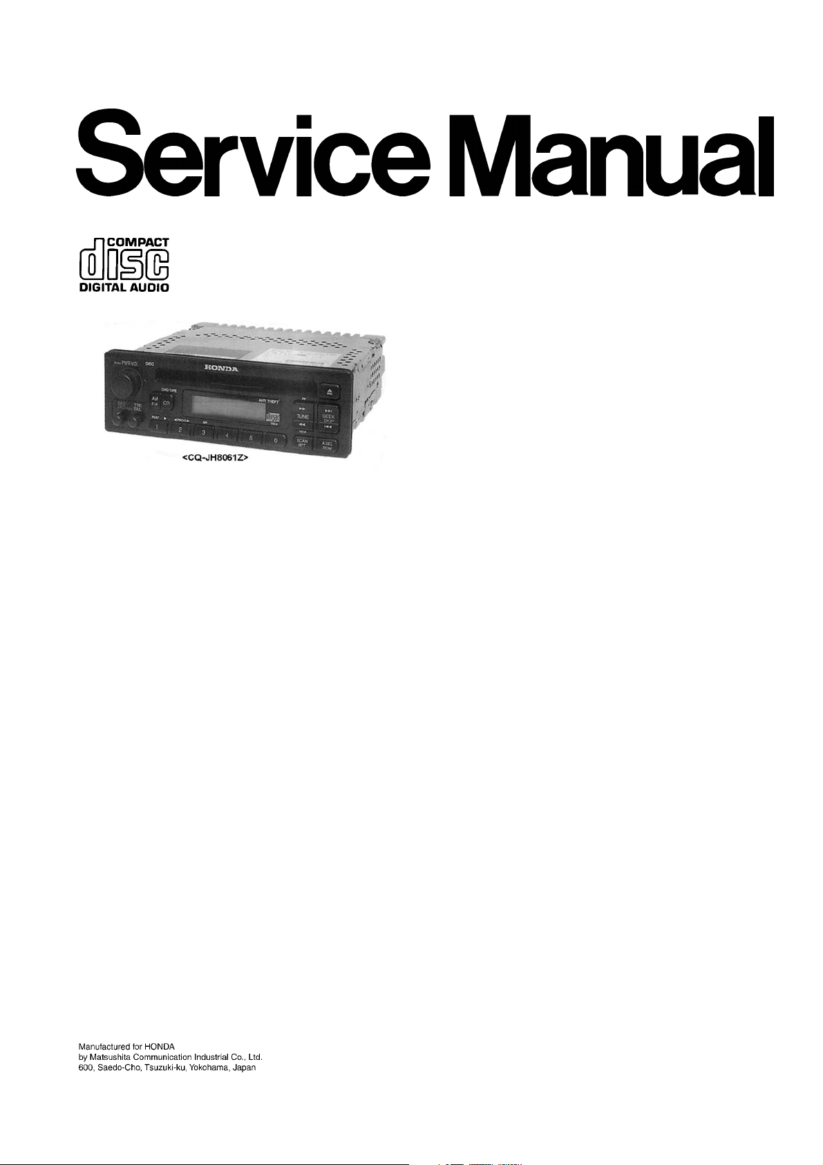
CQ-JH8061Z
CQ-JH8062Z
AM/FM MPX ELECTRONIC TUNING
RADIO with CD Player
PART No. (CQ-JH8061Z) : 39100-S0X-C010
(CQ-JH8062Z) : 39100-S0X-A210
ID CORD : 1XX1
VEHICLE (CQ-JH8061Z) : ODYSSEY
(CQ-JH8062Z) : ODYSSEY (w/NAVI)
DESTINATION : North America
PRODUCED AFTER : Aug., 2000
I0
Specification*
General
Power Supply DC 12V (11V - 16V),
Test Voltage 13.2V
Negative Ground
Current Consumption Less than 3.0A (at 0.5W)
Speaker Output 20W×4ch
Speaker Impedance 4Ω
AM Radio
Frequency Range 530 - 1,710kHz
Usable Sensitivity 24dB/µV (S/N 20dB)
FM Stereo Radio
Frequency Range 87.7 - 107.9MHz
Usable Sensitivity 7dB/µV (S/N 30dB)
CD Player
Signal to Noise Ratio More than 66dB (IHF-A)
Channel Separation More than 50dB (IHF-A)
Dimensions** (W×H×D) 180×172×52mm
Weight** 1.6kg
* Specifications and the design are subject to possible modification
without notice due to improvements.
** Dimensions and Weight shown are approximate.
HONDA / CQ-JH8061Z / CQ-JH806 2Z
CONTENTS
Page Page
1 FEATUERS 2
2 LASER PRODUCTS
3 REAR VIEW AND CONNECTORS
4 FRONT VIEW AND FUNCTIONS
5 WIRING CONNECTIONS
6 BLOCK DIAGRAM (Main Block)
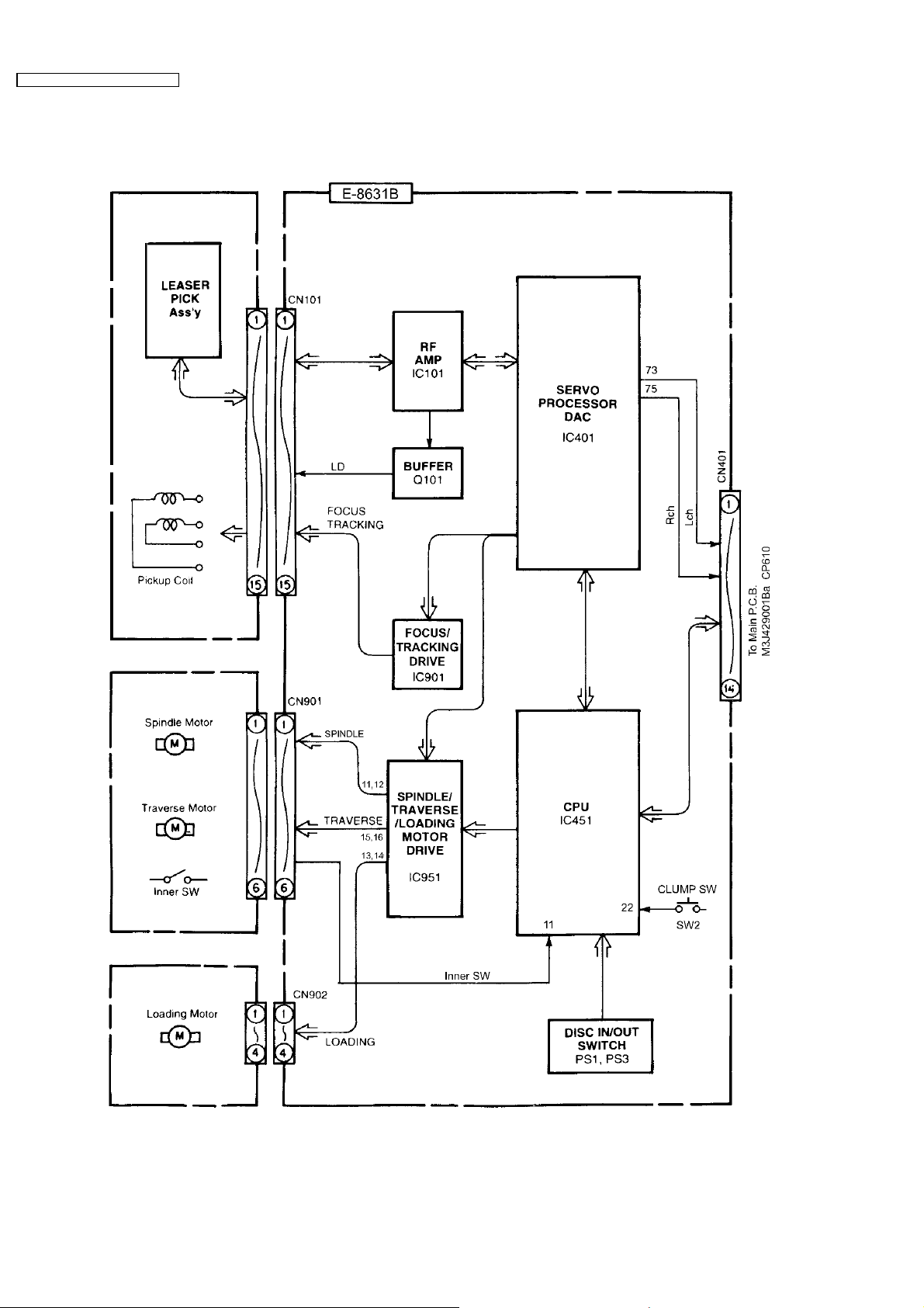
7 BLOCK DIAGRAM (CD Servo Block)
8 TERMINALS DESCRIPTION
9 PACKAGE AND IC BLOCK DIAGRAM 9
2
10 REPLACEMENT PARTS LIST
3
11 EXPLODED VIEW (Unit)
12 CD Player Parts
3
4
13 EXPLODED VIEW (CD Deck)
5
14 WIRING DIAGRAM
15 SCHEMAT IC DIAGRAM -1
6
7
16 SCHEMAT IC DIAGRAM -2
1 FEATUERS
·
PLL (Phase Locked Loop) synthesized tuning.
·
18-station preset (12-FM, 6-AM).
·
CD random, repeat play fnction.
·
Electronic control of power and sound.
·
CD changer control.
·
Anti-Theft system.
13
18
19
21
22
26
27
2 LASER PRODUCTS
2
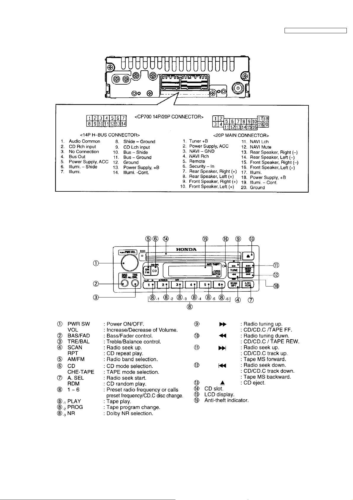
3 REAR VIEW AND CONNECTORS
HONDA / CQ-JH8061Z / CQ-JH806 2Z
4 FRONT VIEW AND FUNCTIONS
3
HONDA / CQ-JH8061Z / CQ-JH806 2Z
5 WIRING CONNECTIONS
4
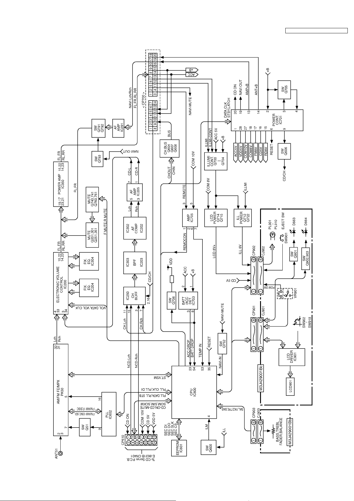
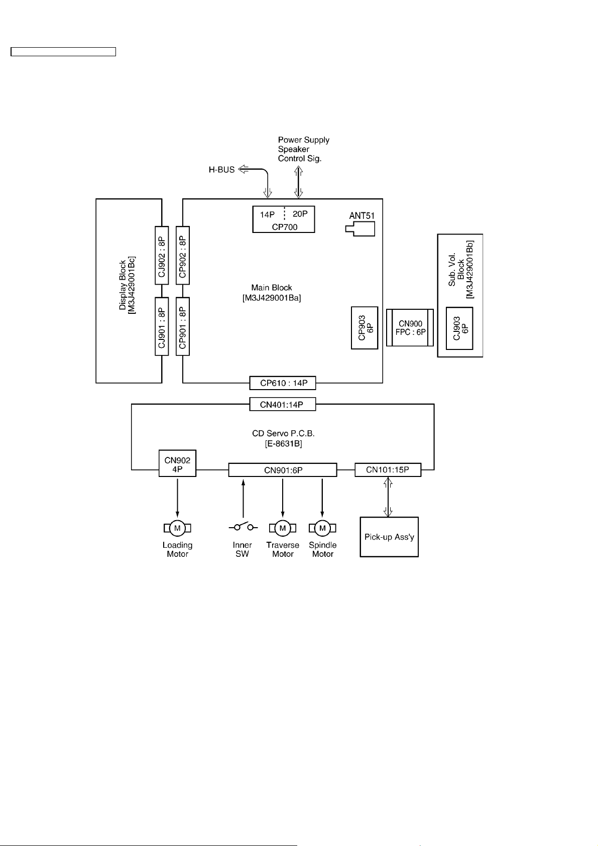
6 BLOCK DIAGRAM (Main Block)
HONDA / CQ-JH8061Z / CQ-JH806 2Z
5
HONDA / CQ-JH8061Z / CQ-JH806 2Z
7 BLOCK DIAGRAM (CD Servo Block)
6
8 TERMINALS DESCRIPTION
HONDA / CQ-JH8061Z / CQ-JH806 2Z
8.1. Main Block
IC600 : C2BBGE000242
Pin
No.
1 /NAVI IN NAVI mute input I 4.5
2 ST IN FM stereo detection I 0.3
3 Ga input (+5V pull-up) I 4.5
4 /ILM Illumination on I 4.5
5 /POW SW Power switch input I 4.2
6 IC CLK Power cont. IC clock O 0
7 BEEP Beep output O 0
8 SEC DI Security data0 output I 0
9 VSS Ground - 0
10 SEC DO Srcurity data output O 0
11 PLL/VOL CLK PLL/Vol. cont clock O 0
12 PLL/VOL DATA PLL/Vol. cont data O 0
13 VOL CLK Vol. cont clock O 0
14 IC STBY Power IC stand-by O 4.9
15 IC DATA Power IC control data O 4.9
16 IC LATCH Power IC data latch O 4.9
17 CH CONT CD changer BUS data O 0
18,19 SET S0, 1 Setting value strobe O 0
20-22 SET R0-2 Setting Value return I 0
23 ACC DROP ACC level detection I 3.8
24 VSS Ground - 0
25 F MUTE Front mute O 0
26 R MUTE Rear mute O 0
27 CD RESET CD reset O 4.0
28 /SEC LED Security LED on/off O 4.7
29 VOL A Rotary encoder signal I 0.8
30 VOL B Rotary encoder signal I 0.8
31 PLL DI PLL data input I 0
32 PLL STB PLL strobe O 0
33 SEC CLK Security clock O 0
34 SEC CS Security IC chip enable O 0
35 /RESET Reset input I 4.4
36 CH IN CD changer detection I 4.7
37 /CD EJECT CD eject SW I 4.4
38 FCONT1 OSC control O 0
39 FCONT2 OSC control O 4.7
40 VDD +5V power supply - 4.9
41 X2 Crystal oscillator - 2.7
42 X1 Crystal oscillator - 1.1
43 IC (VSS) (Connecting to ground) - 0
44 XT2 Crystal oscillator - 2.4
45 XT1 Crystal oscillator - 0.7
46 AVSS Ground - 0
47 V AM/FM Radio signal strongth I 0.2
48 BASS Bass setting level I 2.4
49 TRE Treble setting level I 2.4
50 FAD Fader setting level I 2.4
51 BAL Balance setting level I 2.4
52 RMT CONT Remote control I 5.0
53 TEMP IN Temperature input I 3.0
54 BAT DROP Battery level detection I 4.3
55 AVDD +5V power supply - 4.9
56 AVREF +5V power supply - 5.0
57 LCD DATA LCD data output O 0
58 LCD DI LCD data input I 4.7
59 LCD CLK LCD clock O 0
60 LCD STB LCD strobe O 0
61 TIME ACC (Ground pull-down) - 0
62 SIM CD data input I 0.2
63 SOM CD data output O 1.4
64 SCKM CD data clock O 4.8
Port Descriptions I/O Vol
(V)
8.2. Display Block
IC901 : C0HBA0000017
Pin
No.
1 P1 Disc LED control O 0
2 P2 Illumi. dimmer control O 0
3-8 - No connection - -
9-39 SEG9-39 LCD segment data output O 2.5
40 SEG40 No connection - -
41-43 COM1-3 LCD common output O 2.5
44 S41 No connection - -
45-48 KS2-5 Key scan signal O 0.9
49 KS6 No connection - -
50-53 KI1-4 Key return signal I 0
54 KI5 (Connecting to ground) - 0
55 TEST (Connecting to ground) - 0
56 VDD +5V power supply - 5.1
57 VDD1 Ground through capacitor - 3.3
58 VDD2 Ground through capacitor - 1.7
59 VSS Ground - 0
60 OSC CR oscillator terminal - 3.9
61 DO Key data output O 4.4
62 CE Chip enable I 0
63 CLK LCD clock I 0
64 DI LCD data I 0
Port Descriptions I/O Vol
(V)
Note : Voltage measuerments are with respect to ground, with
a voltmeter (internal resistance : 10M ohms).
7
HONDA / CQ-JH8061Z / CQ-JH806 2Z
8.3. CD Servo Block
IC01 : MN662783RPMF
Pin
No.
1 BCLK (NC) Not used - -
2 LRCK (NC) Not used - -
3 SRDATA (NC) Not used - -
4 DVDD1 +5V power supply for digital
5 DVSS1 Ground - 0
6 TX(NC) Not used - -
7 MCLK Micro computer command clock I 0
8 MDATA Micro computer command data I 1.0
9 MLD Micro computer command load I 4.9
10 SENSE Sence signal O 0
11 /FLOCK Focus servo lock signal O 0
12 /TLOCK Tracking servo lock signal O 0
13 BLKCK(NC) Not used - -
14 SQCK Sub. code-Q reg. clock I 4.9
15 SUBQ Sub. code-Q data O 2.7
16 DMUTE Mute input I 0
17 STAT Status signal O 4.0
18 /RST Reset input I 4.9
19 SMCK(NC) Not used - -
20 PMCK(NC) Not used - -
21 TRV Traverse force feed O 2.5
22 TVD Traverse drive signal O 2.5
23 PC (NC) Not used - -
24 ECM Spindle motor drive signal O 0
25 ECS Spindle motor drive signal O 2.4
26 KICK Kick pulse output O 0
27 TRD Tracking drive signal O 2.5
28 FOD Focus drive signal O 2.5
29 VREF Reference voltage inpu I 2.5
30 FBAL Focus balance adjustment
31 TBAL Tracking balance adjustment
32 FE Focus error signal I 2.4
33 TE Tracking error signal I 2.5
34 RFENV RF envelope signal I 2.5
35 VDET Vibration detection signal I 0
36 OFT Off track signal I 0
37 TRCRS Track cross signal I 0
38 /RFDET RF detection signal I 0
39 BDO Drop out signal I 0
40 LDON Laser on/off O 4.9
41 PLL F2 (NC) Not used - -
42 TOFS TE offset O 2.4
43 WVEL (NC) Not used - -
44 ARF RF signal I 2.5
45 IREF Reference current input I 1.2
46 DRF DSL bias I 2.5
47 DSLF DSL loop filte I/O 2.5
48 PLLF PLL loop filter I/O 1.8
49 VCOF(NC) Not used - -
50 AVDD2 +5V power supply for analog
51 AVSS2 analog logic ground - 0
52 EFM(NC) Not used - -
53 PCK/DSLB DSL bias I 2.4
54 VCOF2 Tracking offset adjustment
55 SUBC(NC) Not used - -
56 SBCK (Conecting to ground) - 0
57 VSS Ground - 0
58 X1 Crystal oscillator terminal I 2.1
59 X2 Crystal oscillator terminal O 2.4
60 VDD +5V power supply - 5.0
61 BYTCK(NC) Not used - -
62 /CLDCK(NC) Not used - -
63 FCLK(NC) Not used - -
64 IP FLAG (NC) Not used - -
65 FLAG(NC) Not used - -
Port Descriptions I/O Vol
logic
output
output
logic
output
(V)
- 5.0
O 2.8
O 2.6
- 5.0
O 2.1
Pin
No.
66 CLVS(NC) Not used - -
67 CRC(NC) Not used - -
68 DEMPH(NC) Not used - -
69 RESY(NC) Not used - -
70 IOSEL (Connecting to VDD) - 5.0
71 /TEST (Connecting to VDD) - 5.0
72 AVDD1 +5V power supply for analog
73 OUTL Audio Lch O 2.4
74 AVSS1 Analog ground - 0
75 OUTR Audio Rch O 2.4
76 RSEL (Connecting to VDD) - 5.0
77 CSEL (Connecting to VDD) I 0
78 PSEL (Conecting to ground) I 0
79 MSEL (Connecting to VDD) I 0
80 SSEL (Connecting to VDD) I 5.0
Port Descriptions I/O Vol
logic
- 4.8
IC451 : MN101C427AE1
Pin
No.
1 MUTE CD mute O 0
2 SCKM Communication clock O 4.8
3 SOM Communication data output O 3.6
4 SIM Communication data input I 0
5 PA0 Ground - 0
6 PA1 Ground - 0
7 PA2 Ground - 0
8 PA3 Ground - 0
9 PA4 Ground - 0
10 PA5 Ground - 0
11 INNER Disc inner SW I 4.9
12 OUT Disc-OUT detection SW I 4.9
13 VDD +5V power supply - 4.9
14 OSC2 Crystal oscillator terminal I 2.4
15 OSC1 Crystal oscillator terminal I 2.4
16 VSS Ground - 0
17 NC Not used - -
18 SBD0 (NC) Not used - -
19 SUB0 Q-code data I 0
20 SQCK Q-code data shift clock I/O 4.9
21 IN Inner SW I 4.9
22 CLUMP Disc clamp SW I 0
23 PC2 Spindle motor drive O 0
24 PC3 Loading motor drive O 4.8
25 LOD Loading motor control O 0
26 BRK Loading motor break control O 0
27 IRQ0 Vibration detection I 0
28 CD.ON CD operation control I 4.9
29 IRQ2 CD operation control I 4.9
30 TRV Traverse motor control O 2.5
31 PC1 Focus/Tracking drive O 4.6
32 BD0 Black spot detection I 0
33 /PRST Servo LSI reset O 4.9
34 STAT Servo LSI status signal I 4.0
35 D.MUTE Servo LSI mute O 0
36 /TLOCK Tracking servo lock detection I 0
37 /FLOCK Focus servo lock detection I 0
38 SENSE Servo LSI status I 0
39 NRST CPU reset I 4.9
40 MMOD (Connecting to ground) - 0
41 P87 Ground - 0
42 MLD Command data latch O 4.9
43 MDATA Command data O 1.0
44 MCLK Command data shift clock O 3.8
Port Descriptions I/O Vol
(V)
(V)
8
 Loading...