

Page 1
ORDER NO.CHM1104021CE
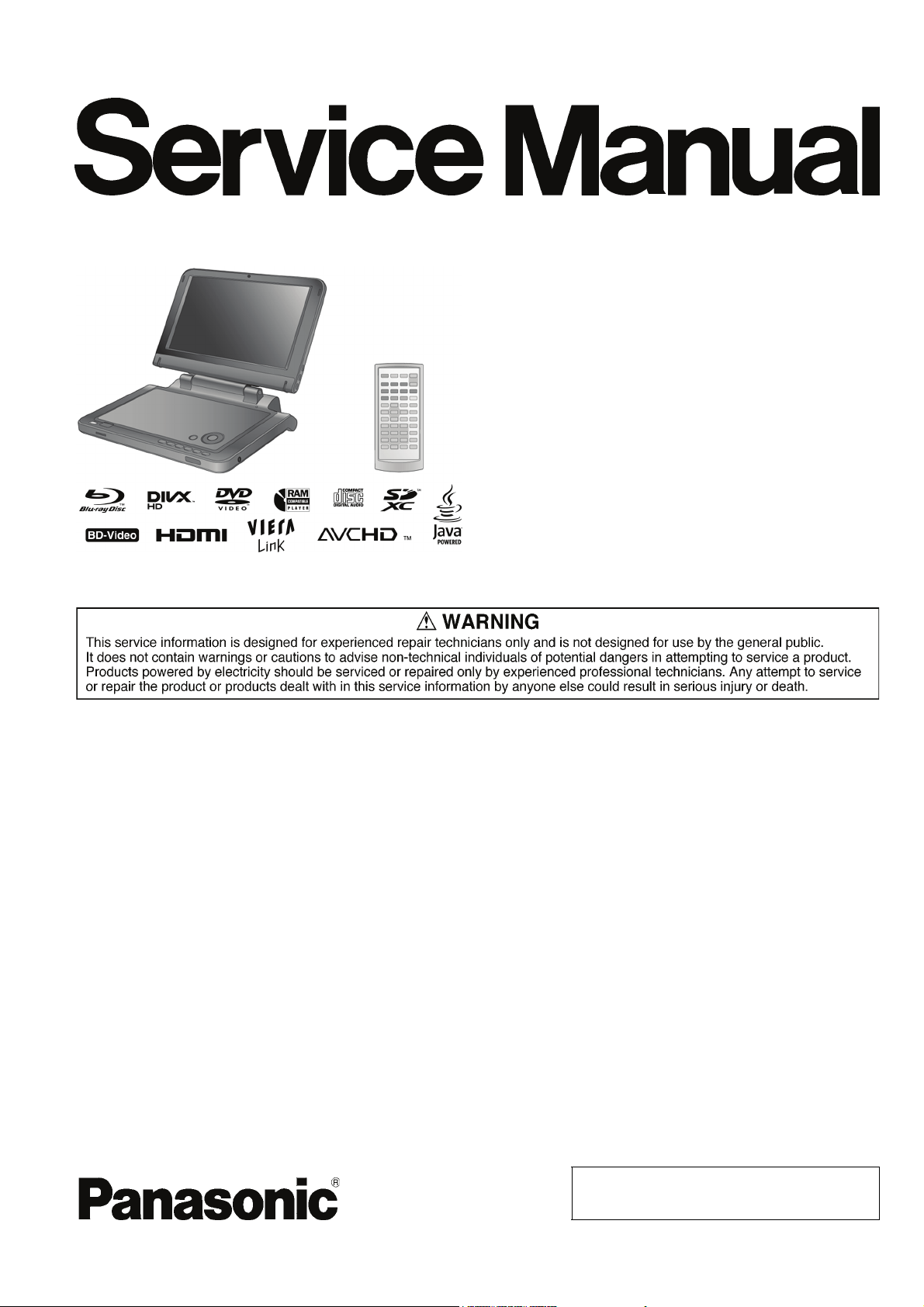
Portable Blu-ray Disc Player
Model No. DMP-B200EB
DMP-B200EE
DMP-B200EG
Vol. 1
Colour
(K).......................Black Type
©Panasonic Corporation 2011.
Unauthorized copying and distribution is a violation
of law.
Page 2

TABLE OF CONTENTS
1 Safety Precautions -----------------------------------------------3
1.1. General guidelines-----------------------------------------3
2Warning--------------------------------------------------------------4
2.1. Prevention of Electrostatic Discharge (ESD)
to Electrostatic Sensitive (ES) Devices---------------4
2.2. How to Replace the Lithium Battery-------------------5
2.3. Caution for AC cord (Only for B200EB) -------------- 6
3 Service Navigation------------------------------------------------7
3.1. Introduction --------------------------------------------------7
3.2. General Description About Lead Free Solder
(PbF) ----------------------------------------------------------7
3.3. Important Notice 1:-----------------------------------------7
3.4. Static Electricity Protection Measures ----------------7
3.5. Ground for electrostatic breakdown
prevention----------------------------------------------------7
3.6. Handling of Traverse unit (optical pick-up) ----------8
3.7. Caution for DivX --------------------------------------------9
4 Specifications ---------------------------------------------------- 10
4.1. Others (Licenses ) ---------------------------------------12
5 Location of Controls and Components ------------------ 13
6 Service Mode ----------------------------------------------------- 15
7 Troubleshooting Guide---------------------------------------- 21
7.1. Self-Diagnosis Functions------------------------------ 21
8 Service Fixture & Tools --------------------------------------- 23
9 Disassembly and Assembly Instructions--------------- 24
9.1. Disassembly Flow Chart--------------------------------24
9.2. P.C.B. location -------------------------------------------- 25
9.3. Main cabinet unit ----------------------------------------- 25
9.4. Traverse Unit ---------------------------------------------- 26
9.5. Main P.C.B. ------------------------------------------------26
9.6. Operation P.C.B. ----------------------------------------- 26
PAGE PAGE
9.7. Disc cover ------------------------------------------------- 26
9.8. Monitor assembly---------------------------------------- 27
9.9. Monitor cover --------------------------------------------- 27
9.10. Mono arm -------------------------------------------------- 28
9.11. LCD panel ------------------------------------------------- 29
9.12. Cleaning of the Optical Pick-up ---------------------- 30
10 Measurements and Adjustments -------------------------- 31
10.1. Service Positions ---------------------------------------- 31
10.2. Caution for Replacing Parts--------------------------- 34
10.3. Adjustment Instruction when Exchange the
OPU Ass'y or Main P.C.B. adjustment value
initialization adjust -------------------------------------- 35
11 Sch ema tic Dia gram -------------------------------------------- 38
11.1. Interconnection Schematic Diagram---------------- 38
11.2. Bat-Connector and Speaker Schematic
Diagram ---------------------------------------------------- 39
11.3. OPERATION Schematic Diagram ------------------- 40
11.4. HP_REMOCON SCHEMATIC DIAGRAM--------- 41
11.5. LCD_SW SCHEMATIC DIAGRAM------------------ 42
12 Printed Circuit Board------------------------------------------ 43
12.1. OPERATION P.C.B.------------------------------------- 43
12.2. HP_REMOCON P.C.B. -------------------------------- 45
12.3. BAT-CONNECTOR P.C.B. ---------------------------- 46
12.4. LCD_SW P.C.B. and SPEAKER P.C.B. ----------- 47
13 Appendix for Schematic Diagram------------------------- 48
13.1. Voltage and Waveform Chart ------------------------- 48
14 Exploded View and Replacement Parts List----------- 51
14.1. Exploded Views and Mechanical
Replacement Parts List -------------------------------- 51
14.2. Electrical Replacement Parts List ------------------- 55
15 Schematic Diagram for printing with A4 size --------- 56
2
Page 3
1 Safety Precautions
1.1. General guidelines
1. IMPORTANT SAFETY NOTICE
There are special components used in this equipment
which are important for safety. These parts are marked by
in the Schematic Diagrams, Circuit Board Layout,
Exploded Views and Replacement Parts List. It is essential that these critical parts should be replaced with manufacturer’s specified parts to prevent X-RADIATION,
shock, fire, or other hazards. Do not modify the original
design without permission of manufacturer.
2. An Isolation Transformer should always be used during
the servicing of AC Adaptor whose chassis is not isolated
from the AC power line. Use a transformer of adequate
power rating as this protects the technician from accidents resulting in personal injury from electrical shocks. It
will also protect AC Adaptor from being damaged by accidental shorting that may occur during servicing.
3. When servicing, observe the original lead dress. If a short
circuit is found, replace all parts which have been overheated or damaged by the short circuit.
4. After servicing, see to it that all the protective devices
such as insulation barriers, insulation papers shields are
properly installed.
5. After servicing, make the following leakage current
checks to prevent the customer from being exposed to
shock hazards.
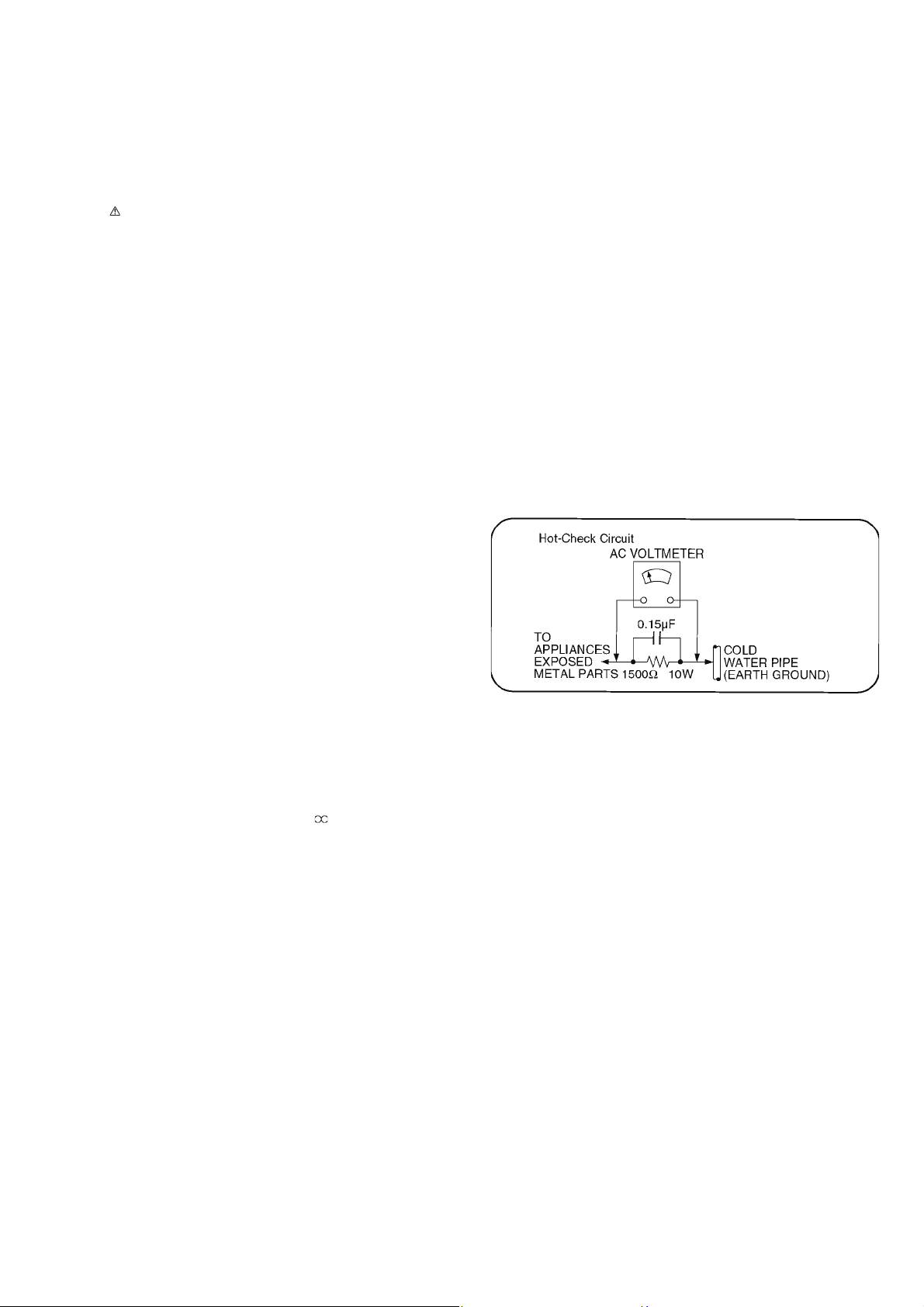
1.1.2. Leakage current hot check (See Figure 1.)
1. Plug the AC cord directly into the AC outlet. Do not use
an isolation transformer for this check.
2. Connect a 1.5kΩ, 10 watts resistor, in parallel with a
0.15μF capacitors, between each exposed metallic part
on the set and a good earth ground such as a water pipe,
as shown in Figure 1.
3. Use an AC voltmeter, with 1000 ohms/volt or more sensitivity, to measure the potential across the resistor.
4. Check each exposed metallic part, and measure the voltage at each point.
5. Reverse the AC plug in the AC outlet and repeat each of
the above measurements.
6. The potential at any point should not exceed 0.75 volts
RMS. A leakage current tester (Simpson Model 229 or
equivalent) may be used to make the hot checks, leakage
current must not exceed 1/2 milliampere. In case a measurement is outside of the limits specified, there is a possibility of a shock hazard, and the equipment should be
repaired and rechecked before it is returned to the customer.
1.1.1. Leakage current cold check
1. Unplug the AC cord and connect a jumper between the
two prongs on the plug.
2. Measure the resistance value, with an ohmmeter,
between the jumpered AC plug and each exposed metallic cabinet part on the equipment such as screwheads,
connectors, control shafts, etc. When the exposed metallic part has a return path to the chassis, the reading
should be between 1MΩ and 5.2MΩ.
When the exposed metal does not have a return path to
the chassis, the reading must be .
3
Page 4

2Warning
2.1. Prevention of Electrostatic Discharge (ESD) to Electrostatic Sensitive (ES) Devices
Some semiconductor (solid state) devices can be damaged easily by static electricity. Such components commonly are called Electrostatic Sensitive (ES) Devices. Examples of typical ES devices are integrated circuits and some field-effect transistors and semiconductor "chip" components. The following techniques should be used to help reduce the incidence of component damage
caused by electrostatic discharge (ESD).
1. Immediately before handling any semiconductor component or semiconductor-equipped assembly, drain off any ESD on your
body by touching a known earth ground. Alternatively, obtain and wear a commercially available discharging ESD wrist strap,
which should be removed for potential shock reasons prior to applying power to the unit under test.
2. After removing an electrical assembly equipped with ES devices, place the assembly on a conductive surface such as aluminum foil, to prevent electrostatic charge buildup or exposure of the assembly.
3. Use only a grounded-tip soldering iron to solder or unsolder ES devices.
4. Use only an anti-static solder removal device. Some solder removal devices not classified as "anti-static (ESD protected)" can
generate electrical charge sufficient to damage ES devices.
5. Do not use freon-propelled chemicals. These can generate electrical charges sufficient to damage ES devices.
6. Do not remove a replacement ES device from its protective package until immediately before you are ready to install it. (Most
replacement ES devices are packaged with leads electrically shorted together by conductive foam, aluminum foil or comparable conductive material).
7. Immediately before removing the protective material from the leads of a replacement ES device, touch the protective material
to the chassis or circuit assembly into which the device will be installed.
Caution
Be sure no power is applied to the chassis or circuit, and observe all other safety precautions.
8. Minimize bodily motions when handling unpackaged replacement ES devices. (Otherwise harmless motion such as the
brushing together of your clothes fabric or the lifting of your foot from a carpeted floor can generate static electricity sufficient
to damage an ES device).
4
Page 5
2.2. How to Replace the Lithium Battery
This model is using a lithium battery for remote control ass’y.
NOTE:
This Lithium battery is a critical component.
(Type No.: CR2025 Manufactured by Energy Company, Panasonic Corporation.)
It must never be subjected to excessive heat or discharge.
It must therefore only be fitted in requirement designed specifically for its use.
Replacement batteries must be of same type and manufacture.
They must be fitted in the same manner and location as the original battery, with the correct polarity contacts observed.
Do not attempt to re-charge the old battery or re-use it for any other purpose.
It should be disposed of in waste products destined for burial rather than incineration.
5
Page 6
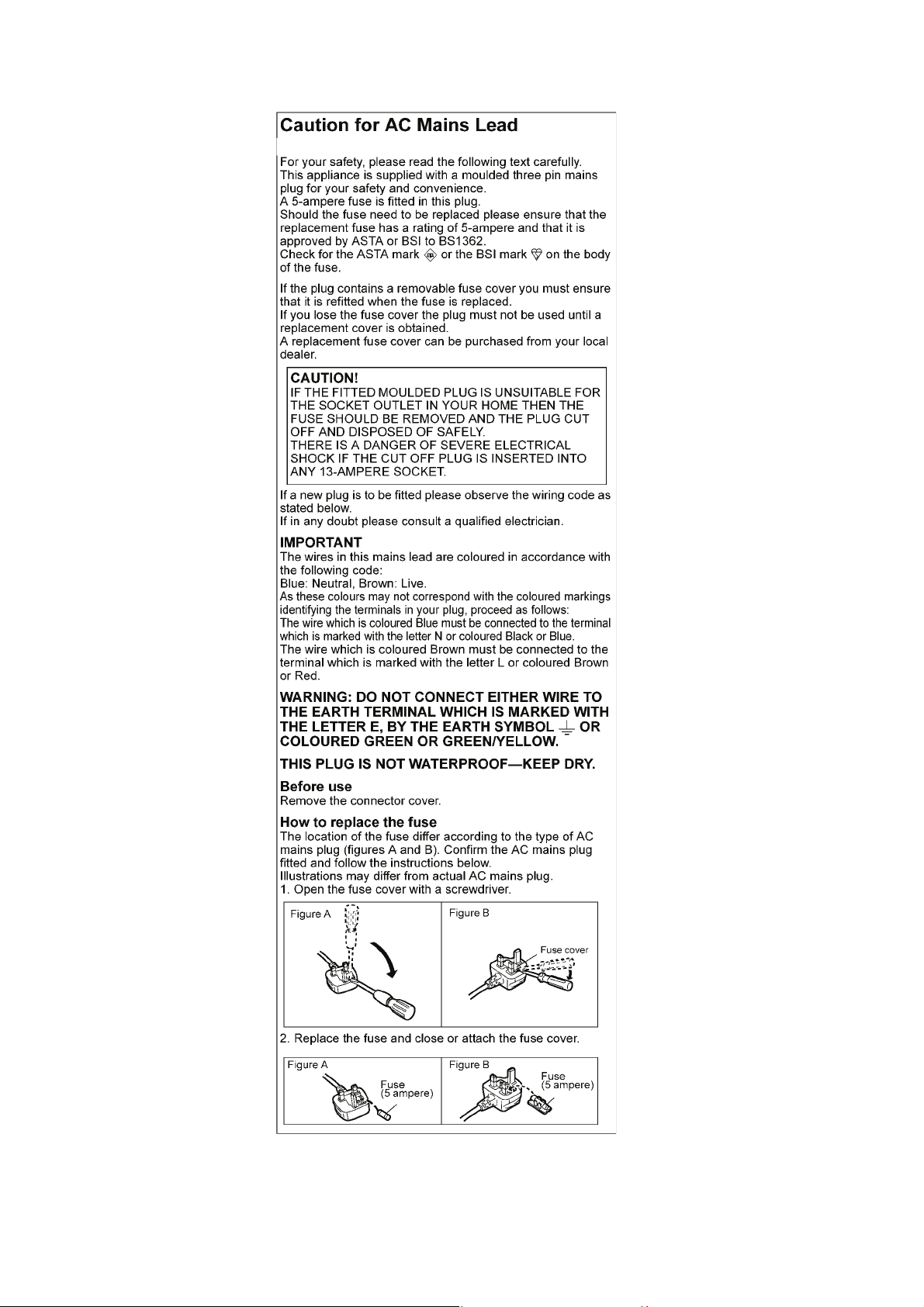
2.3. Caution for AC cord (Only for B200EB)
6
Page 7
3 Service Navigation
3.1. Introduction
This service manual contains technical information, which allow service personnel's to understand and service this model.
Please place orders using the parts list and not the drawing reference numbers.
If the circuit is changed or modified, the information will be followed by service manual to be controlled with original service manual.
3.2. General Description About Lead Free Solder (PbF)
The lead free solder has been used in the mounting process of all electrical components on the printed circuit boards used for this
equipment in considering the globally environmental conservation.
The normal solder is the alloy of tin (Sn) and lead (Pb). On the other hand, the lead free solder is the alloy mainly consists of tin
(Sn), silver (Ag) and Copper (Cu), and the melting point of the lead free solder is higher approx.30 degrees C (86°F) more than that
of the normal solder.
Definition of PCB Lead Free Solder being used
The letter of “PbF” is printed either foil side or components side on the PCB using the lead free solder.
(See right figure)
Service caution for repair work using Lead Free Solder (PbF)
• The lead free solder has to be used when repairing the equipment for which the lead free solder is used.
(Definition: The letter of “PbF” is printed on the PCB using the lead free solder.)
• To put lead free solder, it should be well molten and mixed with the original lead free solder.
• Remove the remaining lead free solder on the PCB cleanly for soldering of the new IC.
• Since the melting point of the lead free solder is higher than that of the normal lead solder, it takes the longer time to melt the
lead free solder.
• Use the soldering iron (more than 70W) equipped with the temperature control after setting the temperature at 350±30 degrees
C (662±86°F).
Recommended Lead Free Solder (Service Parts Route.)
• The following 3 types of lead free solder are available through the service parts route.
RFKZ03D01KS-----------(0.3mm 100g Reel)
RFKZ06D01KS-----------(0.6mm 100g Reel)
RFKZ10D01KS-----------(1.0mm 100g Reel)
Note
* Ingredient: tin (Sn), 96.5%, silver (Ag) 3.0%, Copper (Cu) 0.5%, Cobalt (Co) / Germanium (Ge) 0.1 to 0.3%
3.3. Important Notice 1:
1. The service manual does not contain the following information, because of the impossibility of servicing at component level
without concerned equipment/facilites.
a. Schematic diagram, Block Diagram and PCB layout of MAIN PCB.
b. Parts list for individual parts for MAIN PCB.
2. The following category is/are recycle module part. please send it/them to Central Repair Center.
• TRV/MAIN PCB MODULE (B200EB:RFKNB200EB, B200EE:RFKNB200EE, B200EG:RFKNB200EG)
3. When "JIG & ADJ" of pairing adjustment is available:
The Traverse and main P.C.B for PBD model is offered respectively for the market maintenaince.
For the information about pairing adjustment of the Traverse and main P.C.B.,please refer to "10.3 Adjustment Instruction
when Exchange the OPU Ass'y or Main P.C.B. adjustment value initialization adjust" .
3.4. Static Electricity Protection Measures
• The laser diode in the traverse unit (optical pick-up) may break down due to potential difference caused by static electricity of
clothes or human body.
So, be careful of electrostatic breakdown during repair of the traverse unit (optical pick-up).
3.5. Ground for electrostatic breakdown prevention
• As for parts that use optical pick-up (laser diode), the optical pick-up is destroyed by the static electricity of the working environment.
Repair in the working environment that is grounded.
7
Page 8
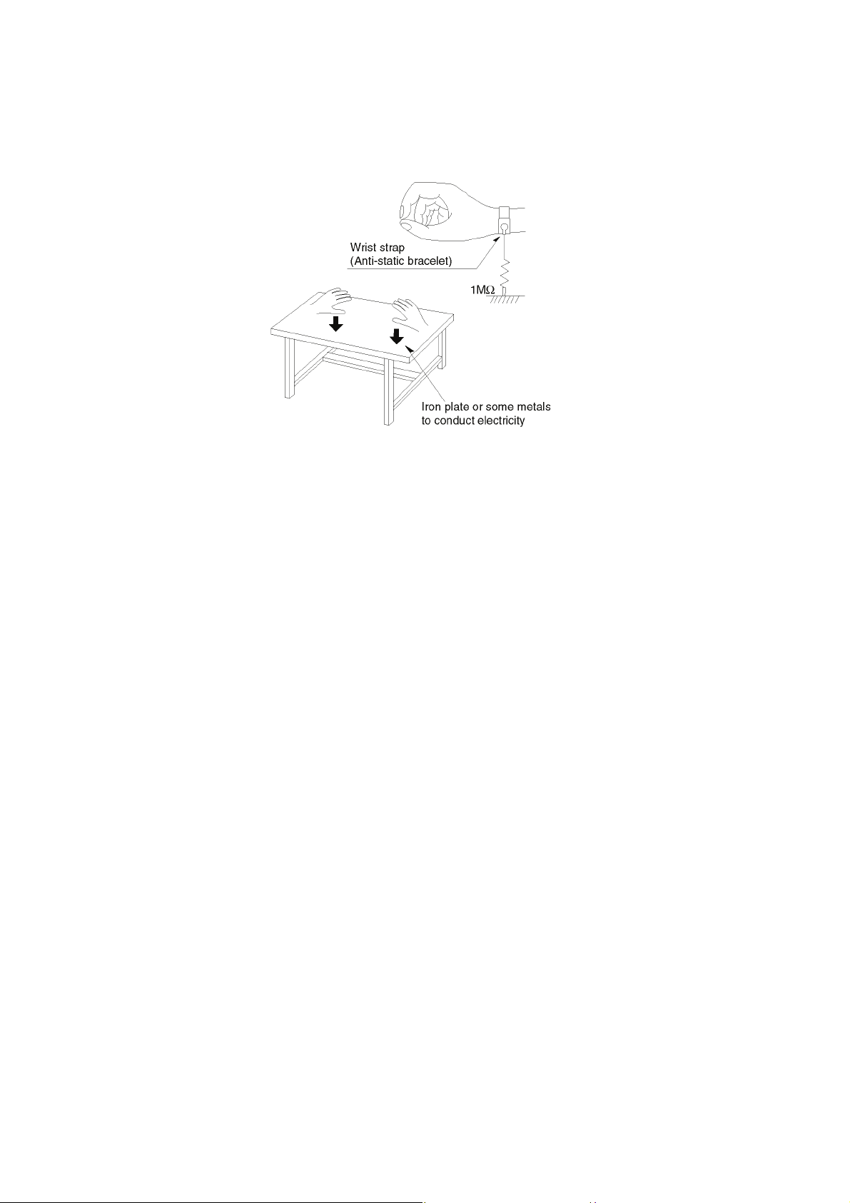
3.5.1. Work table grounding
• Put a conductive material (sheet) or steel sheet on the area where the traverse unit (optical pick-up) is placed, and ground the
sheet.
3.5.2. Human body grounding
• Use the anti-static wrist strap to discharge the static electricity from your body.
3.6. Handling of Traverse unit (optical pick-up)
1. Do not subject the traverse unit (optical pick-up) to hard shock as it is high precision mechanism.
2. Install the traverse unit, and then remove the short pin to discharge.
Connect the connector in a short time.
3. Take care not to apply excessive stress to the flexible cable.
4. Do not turn the variable resistor (laser power adjustment).
It has already been adjusted.
8
Page 9
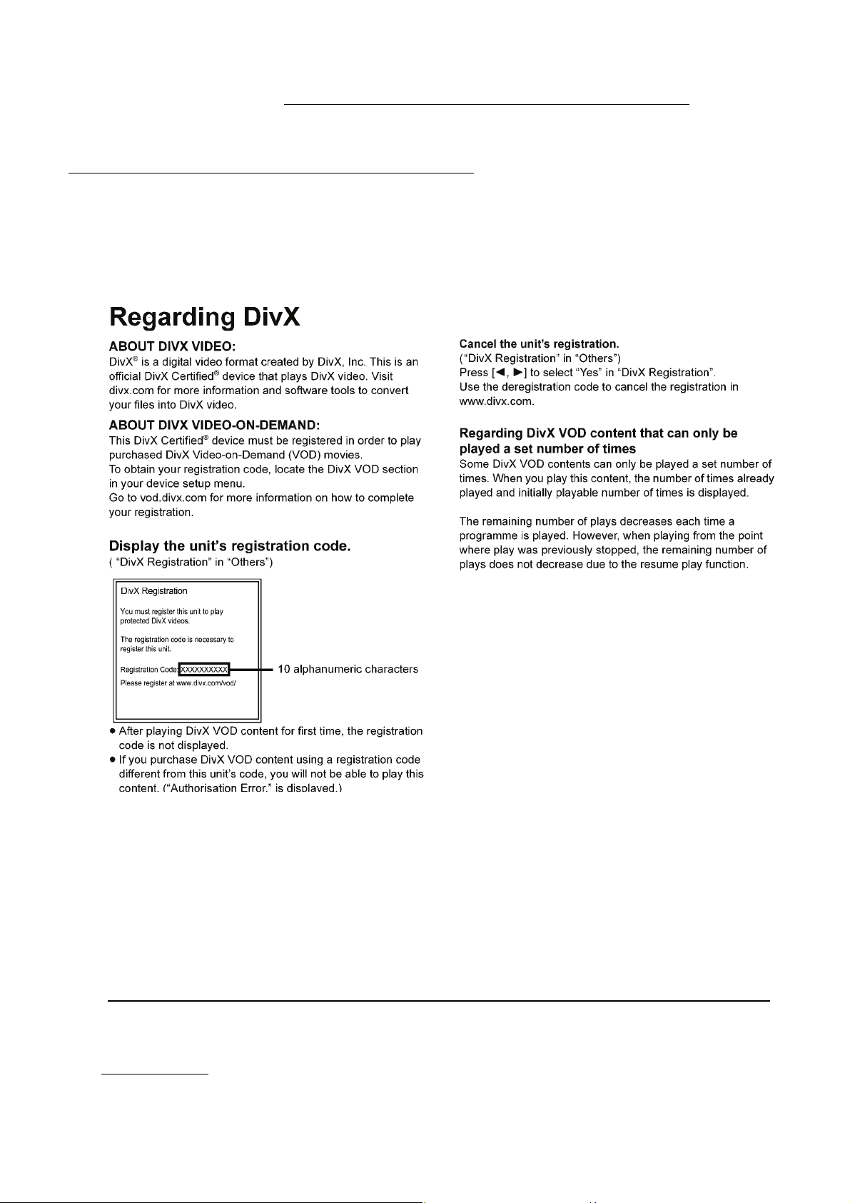
3.7. Caution for DivX
Please will always pass the customer “Warning for Customers Who Use the DivX Video-on-Demand content.” with the product and
get it when you unavoidably exchange FLASH-ROM or P.C.B. including FLASH-ROM (When the product is exchanged, it is the
same.).
You must use print attached to service part (FLASH-ROM or P.C.B. including FLASH-ROM) or must use copy of print below as
“Warning for Customers Who Use the DivX Video-on-Demand content.”
Information needed without fail for the customer for whom it is used continuing DivX Video-on-Demand Service to “Manual for the
customer” is recorded.
Appendix:
*Parts that memorize user’s information are only FLASH-ROM.
*The registration of Registration Code is possible for half a year up to 6 recorders up to 10 recorders a year.
Registration Code is memorized in FLASH-ROM (Main P.C.B.).
If exchange above P.C.B. or FLASH-ROM, new registration Code differ from previous Registration Code will be generated.
In this case if your customer uses DivX Video-on-Demand service, he/she will no longer be able to play any content that he/she purchased under that same registration code.
Therefore your customer will need to obtain and register the new registration code.
*Copy this page and cut on the dotted line and give the lower half to your customer.
-----------------------------------------------------------------------------------------------------------------------------------------------------------------------------
Warning for Customers Who Use the DivX Video-on-Demand content.
1. The registration code has been changed for the repair of the product or the product exchange.
2. Obtain and register a new registration code, otherwise you will no longer be able to play DivX Video-on-Demand content.
3. Follow the procedure on the DivX Video-on-Demand web site to register at
vod.divx.com
http://
* If you do not use the DivX Video-on-Demand content, please ignore this warning.
9
Page 10

4 Specifications
Power supply: DC12V(DC IN terminal)
DC7.2V
(Exclusive battery terminal)
Power consumption:
Play Mode: Approx. 15W
(Unit only approx.12W)
Recharge Mode:
(Quick Start [OFF]):
Recharge Mode:
(Quick Start [ON]):
Standby Mode:
(Quick Start [OFF]):
Standby Mode:
(Quick Start [ON]):
(using included AC adaptor)
AC Adaptor:
Power source: 110V-240V, 50/60Hz
Power consumption: 36W
DC output: 12V, 2000mA
Car DC Adaptor:
DC output: 12V, 2A
Battery pack
DY-DB20(lithium ion):
Voltage: 7.2V
Capacity: 4500mAh(typ)
Dimensions
(excluding protrusions and
battery):
(WxDxH):
Mass:
Including battery: approximately 1371g [48.36oz]
Without battery: approximately 1138g [40.15oz]
Operating temperature range: +5°C to +35°C(+41 to +95°F)
Operating humidity range: 10% - 80%RH (no condensation)
LCD screen:
HDMI
AUDIO/VIDEO output:
number of terminals: 1 system
Speaker:
output: 0.5W + 0.5W (8Ω)
Head phone output:
output:
number of terminals: 1 system
Battery duration
(at 20°C, ECO-charge OFF)
Option Battery pack:
DY-DB30
DY-DB300
*Using headphones
*Battry duration in the ECOcharge ON is about 80% when
charging in the ECO-charge
OFF
when brightness is set to
"-5" while playing DISC:
when brightness is set to
"0" while playing DISC:
when brightness is set to
"+5" while playing DISC:
Battery recharge time:
(at 20°C)
Approx. 18W
Approx. 22W
Approx. 0.4W
Approx. 4.5W
Vehicle with 12V battery only
4200mAh(min)
31Wh
238mm x 188.3mm x 52.7mm
3
(9
/8" x 713/32" x 21/16")
8.9" -Si, TFT wide-screen LCD
(1024 x 600 x RGB)
stereo mini-jack( 3.5mm)
4 hours/5 hours (DY-DB30)/
8 hours (DY-DB300)
3.5 hours/4.5 hours (DY-DB30)/
7 hours (DY-DB300)
3 hours/3.75 hours (DY-DB30)/
6 hours (DY-DB300)
ECO-charge OFF: 4 hours/5 hours (DY-DB30)/
7 hours (DY-DB300)
ECO-charge ON: 3.25 hours/4 hours (DY-DB30)/
Pickup:
Wave Length: 405nm/660nm/780nm (BD/DVD/
Laser power: CLASS 1M/CLASS 1M/
Regional Code: DVD: EB/EG: #2/ EE: #5
Media:
Playable disc:
BD-Video: BD-ROM Version2
BD-RE: Version3 (SL:Single Layer/
BD-R:
DVD-RAM: DVD Video Recording format,
DVD-R: DVD-Video format (*1), DVD
DVD-R DL: DVD-Video format (*1), DVD
DVD-RW: DVD-Video format (*1), DVD
+R: Video(*1), AVCHD format(*1)
+R DL: Video(*1), AVCHD format(*1)
+RW: Video(*1), AVCHD format(*1)
DVD-VIDEO: DVD-Video format
CD-Audio: CD-DA
CD-R/CD-RW: CD-DA, JPEG(*2), MP3(*2),
*1: Finalizing is necessary.
*2: ISO9660 level1 or 2(except for extended formats), Joliet.
This unit is compatible with multi-session.
This unit is not compatible with packet writing.
*3: CPRM discs are not supported.(B200EB/EE)
*4: UDF1.02 without ISO9660, UDF1.5 with ISO9660.
*5: UDF2.5.
*6: DivX Certified to play Divx video up to HD 1080p, including
premium content.
GMC(Global Motion Compensation) is not supported.
*7: Maximum number of folders recognizable:300 folders.
(including the root folder)
Maximum number of files recognizable:200 files.
*8: MPEG-4 AVC (H.264) profile is up to High Profile, Level 4.
AAC-LC, MP3, Dolby Digital audio can be decoded.
SD card:
SD Memory Card(*9)
formatted FAT12, FAT16,
FAT32(*10),exFAT(*11):
*9: includes SDHC, SDXC card..
includes miniSD
includes microSD/microSDHC/micro SDXC Card.
(need a microSD Adaptor.)
*10: Not support long file name.
*11: SDXC only.
Contents:
Card(need a miniSD Adaptor.)
5.5 hours (DY-DB300)
CD)
CLASS 1M (BD/DVD/CD)
BD: EB/EG: Region B
EE: Region C
DL:Dual Layer), JPEG
Version2 (SL:Single Layer/D L:Dual
Layer),
DivX (*5), (*6), (*7),
MKV (*6), (*7), (*8)
AVCHD format, JPEG
Video Recording format(*1),
(
EB/EE:
*3) AVCHD format(*1),
JPEG(*2), MP3(*2),DivX (*2), (*4),
(*6), (*7), MKV (*2), (*4), (*7), (*8)
Video Recording format(*1),
(
EB/EE:
*3) AVCHD format(*1),
JPEG(*2), MP3(*2),DivX (*2), (*4),
(*6), (*7), MKV (*2), (*4), (*6), (*7)
Video Recording format(*1),
EB/EE:
*3) AVCHD format(*1)
(
DivX (*2), (*6), (*7),MKV (*2), (*7),
(*8)
JPEG, AVCHD format, MPEG-2
10
Page 11

JPEG :
SD card, CD-R/RW, DVD-RAM, BD-RE, DVD-R:
Pixcels: 34x34~8192x8192
Sub Sampling: 4:2:2, 4:2:0
Motion JPEG not supproted
SD card: JPEG conforming DCF(Design
rule for Camera File system)
Thawing Time: approx. 2sec (7M pixels,)
Maximum numbers of folders and files:
MP3:
CD-R, CD-RW, DVD-R:
Compression rate: 32kbps~320kbps
Sampling rate: 44.1kHz, 48kHz
AVCHD (H.264):
SD card, DVD: AVCHD format V1.0
HDMI: 480p(525p) / 576p(625p) /
1080i(1125i) / 720p(750p) /
1080p(1125p)HDMI (x.v.Color
High Bit rate Audio)
(This unit supports “HDAVI
Control 5” function.)
Solder: This model uses lead free
solder(PbF).
Note: Specifications are subject to
change without notice.
TM
,
11
Page 12
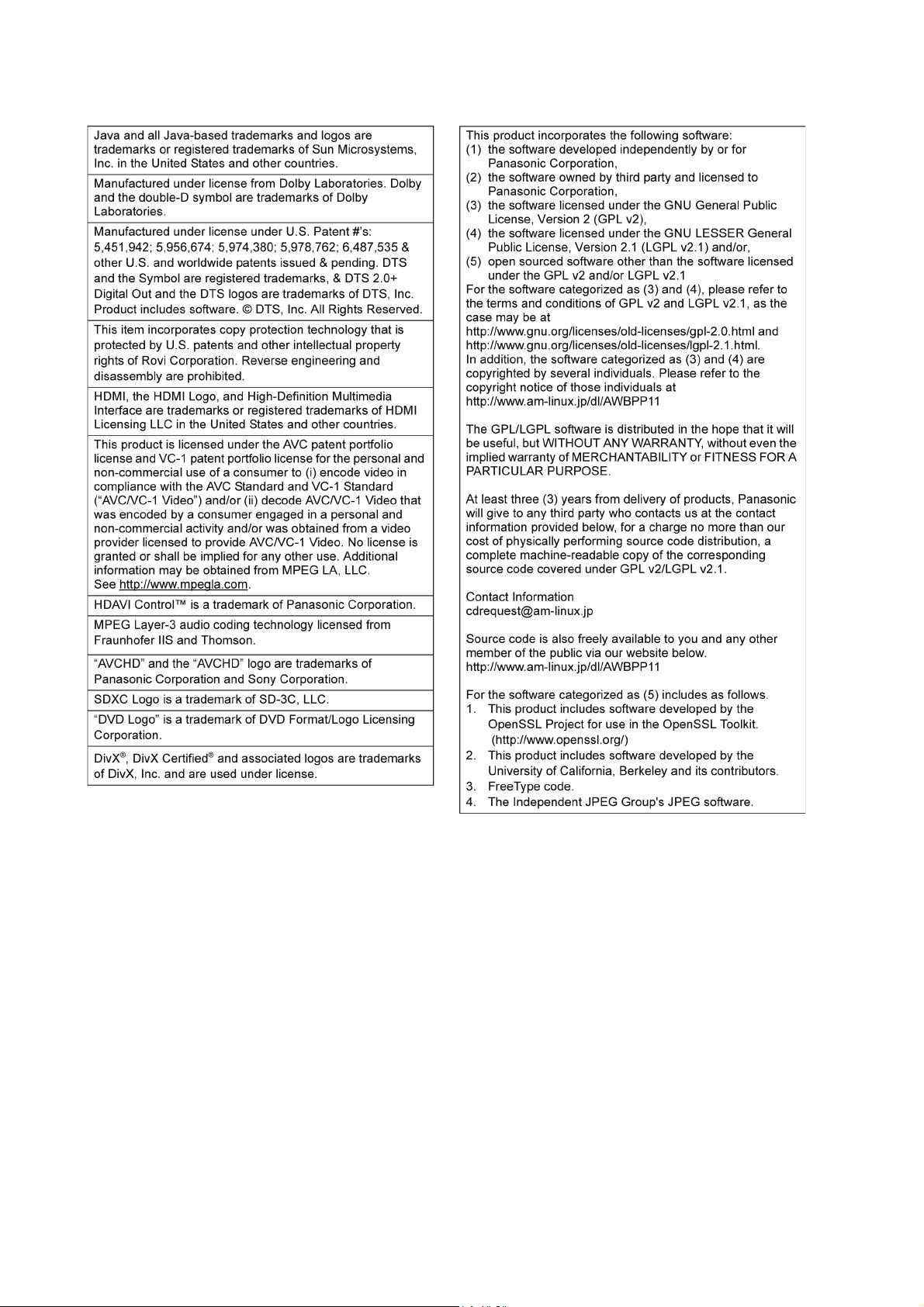
4.1. Others (Licenses )
12
Page 13
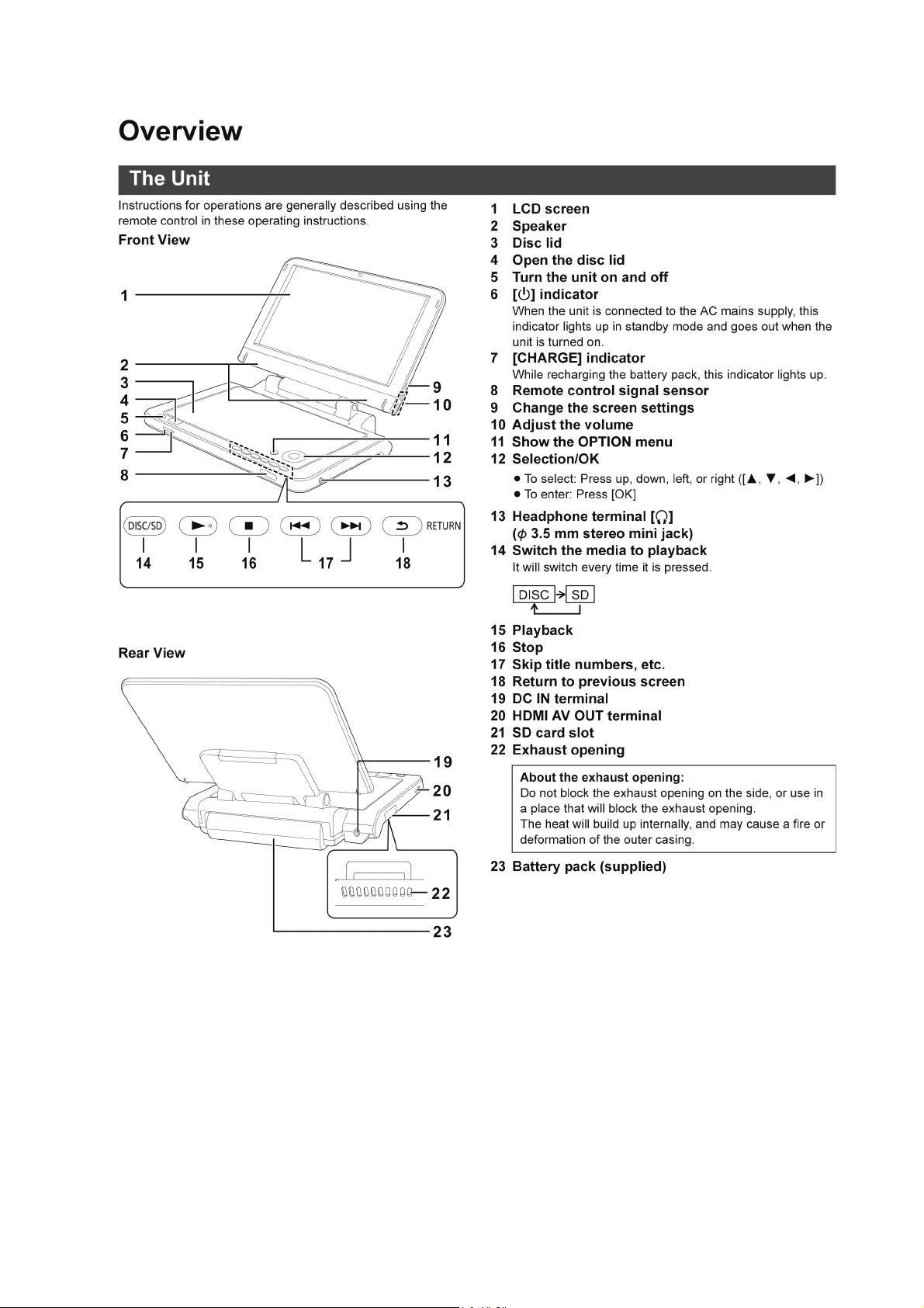
5 Location of Controls and Components
13
Page 14
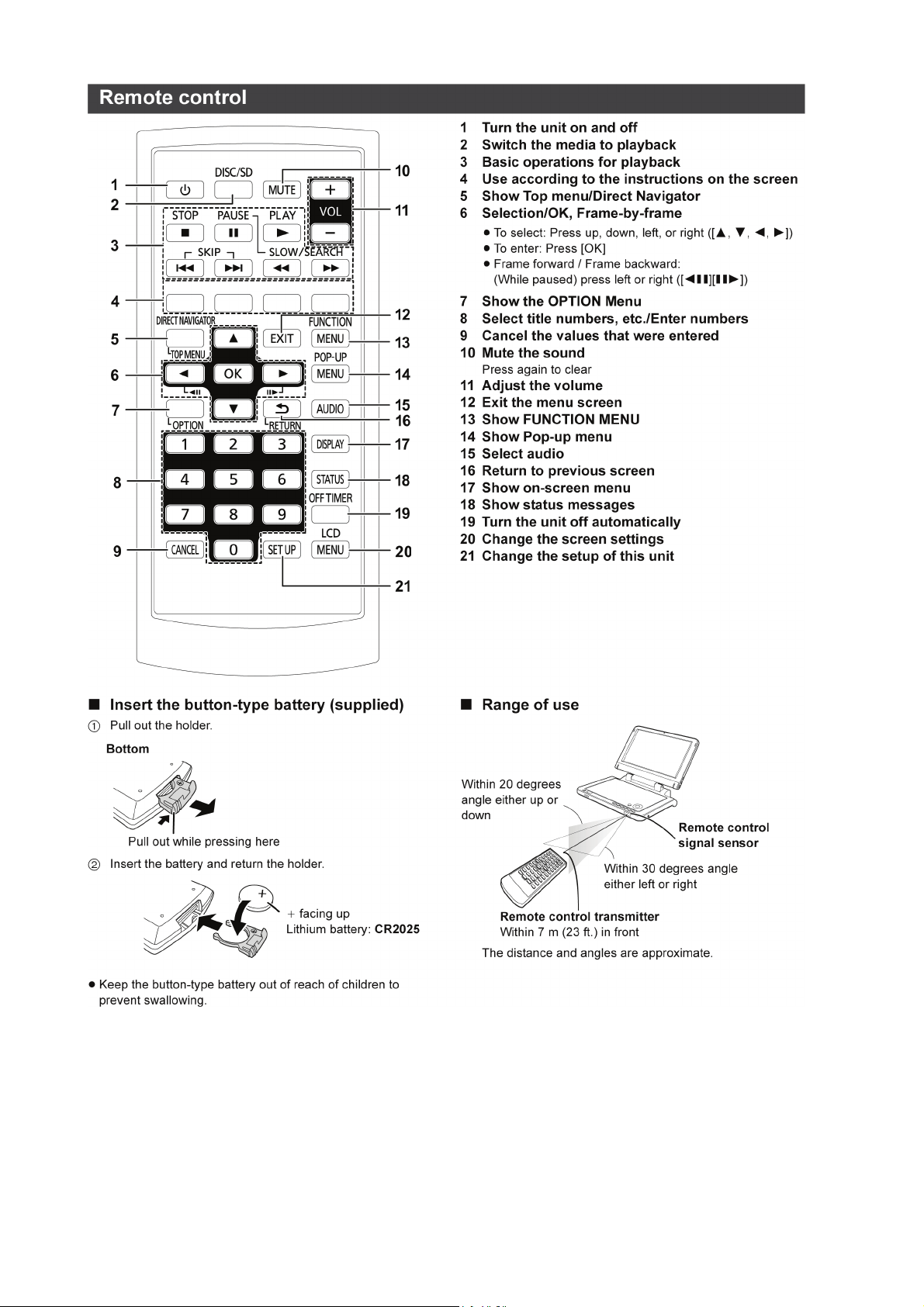
14
Page 15
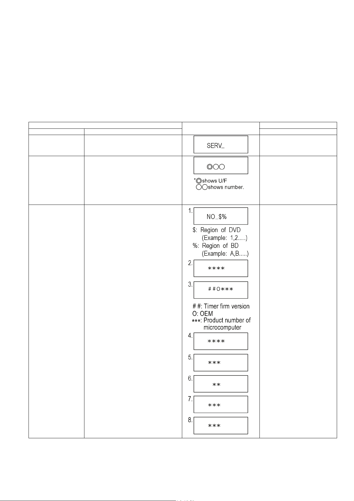
6 Service Mode
Information necessary for service can be displayed.
Service mode setting:
1. Turn the power off.
2. Press the [OPTION] + [PLAY] and [VOL DOWN] button simultaneously for five seconds.
3. It is displayed on LCD as [SERV]. : It is shown to have entered the service mode.
4. The command is transmitted by attached remote control.
Method of making clear service mode : Press the power button (power off).
The display of information to each command is as follows.
NOTE:
Do not use it excluding the designated command.
Item LCD display Key operation
Mode name Description (Remote controller key)
Release Items Item of Service Mode executing is cancelled. Press[0][0] or [Return] in service
mode.
Error Code Display Last Error Code of U/F held by memory is dis-
played on FL.
*Details are described in "Self-Diagnosis
Functions".
7.1. Self-Diagnosis Functions.
ROM Version Display The display contents are switched over every
5 seconds.
1. Region code
2. Main firm version
3. Timer firm version
4. Drive firm version
5. ROM PATCH version
6. Mstar firm version
7. BOOT2 version
8. BOOT3 version
Press [0] [1] in service mode.
If any error history does not exist,
[F00] is displayed.
Press [0] [2] in service mode.
15
Page 16
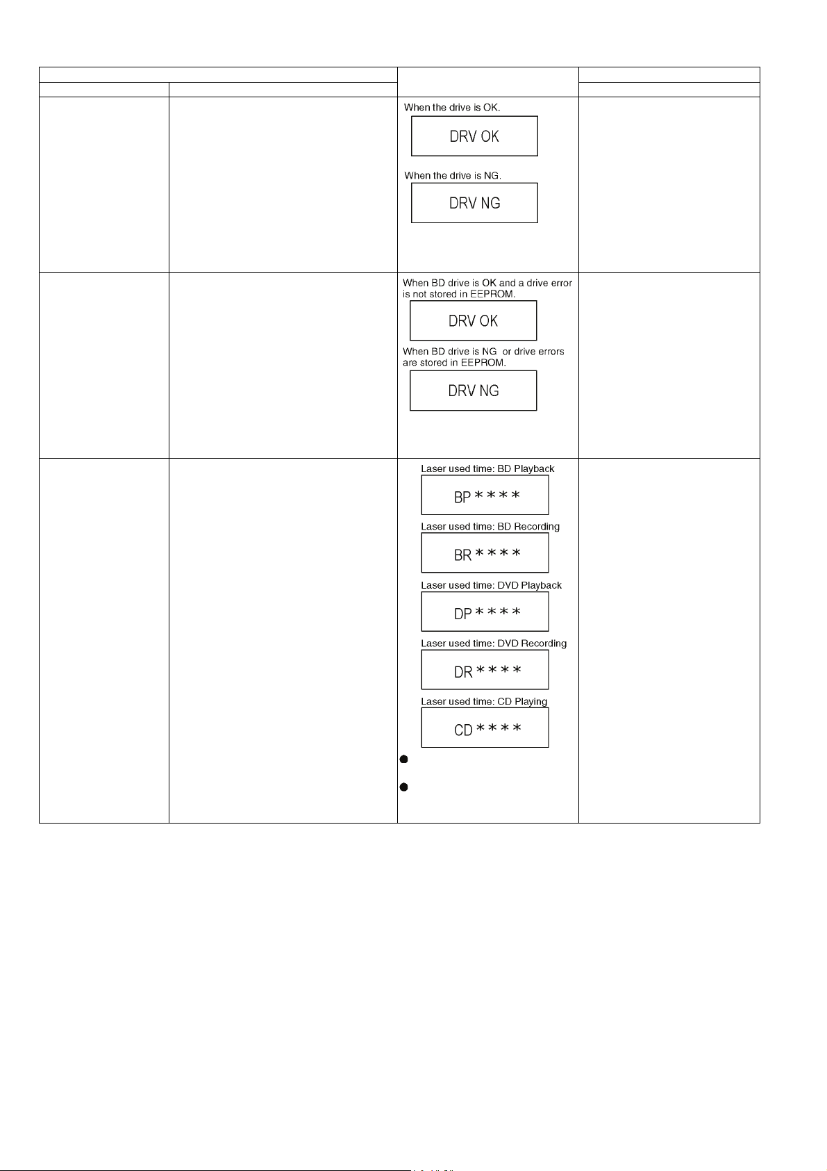
Item LCD display Key operation
Mode name Description (Remote controller key)
Drive Check Simple quality of BD drive
Drive Check Simple quality of BD drive
Laser Used Time
Indication
Check laser used time (hours) of drive.
*If the date of the present or the
trouble occurred time is incorrect, it
may be not able to judge correctly.
*If the date of the present or the
trouble occurred time is incorrect, it
may be not able to judge correctly.
Press [0] [3] in service mode.
Press [3] [8] in service mode.
Press [4] [1] in service mode.
(****) is the used time display in
hour.
Laser used time of BD/ DVD/ CD
in Playback/Recording mode is
counted.
16
Page 17
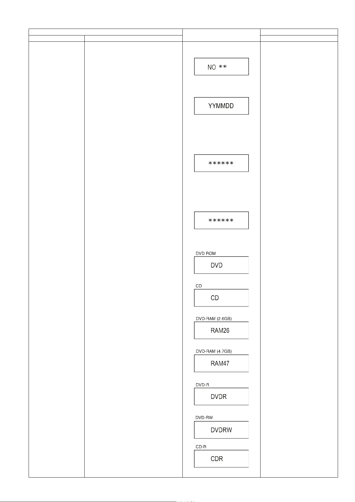
Item LCD display Key operation
Mode name Description (Remote controller key)
BD drive last error BD drive error code display. 1. Error Number is displayed for 5
seconds.
2. Time when the error has occurred
is display for 5 seconds.
YY: Year
MM: Month
DD: Day
3. Last drive error (1/2) is displayed
for 5 seconds.
00 : Bad disc
03 : Bad disc
04 : Bad disc or drive malfunction
4. Last drive error (2/2) is displayed
for 5 seconds.
Press [4] [2] in service mode.
5. Error occurring disc type is displayed for 5 seconds.
17
Page 18
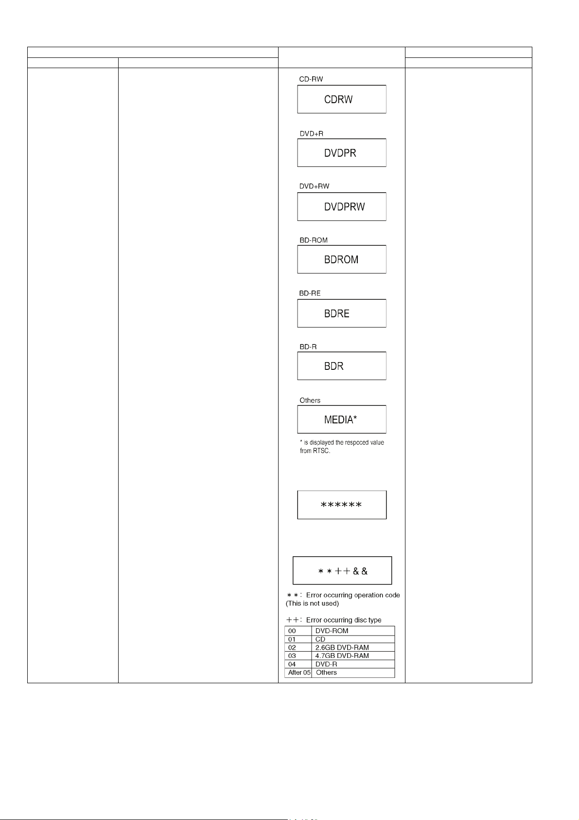
Item LCD display Key operation
Mode name Description (Remote controller key)
6. Disc maker ID is displayed for 5
seconds.
7. Factor of drive error (hexadecimal) occurring is left displayed.
In case that the maker cannot be
identified, display is blackout.
18
Page 19
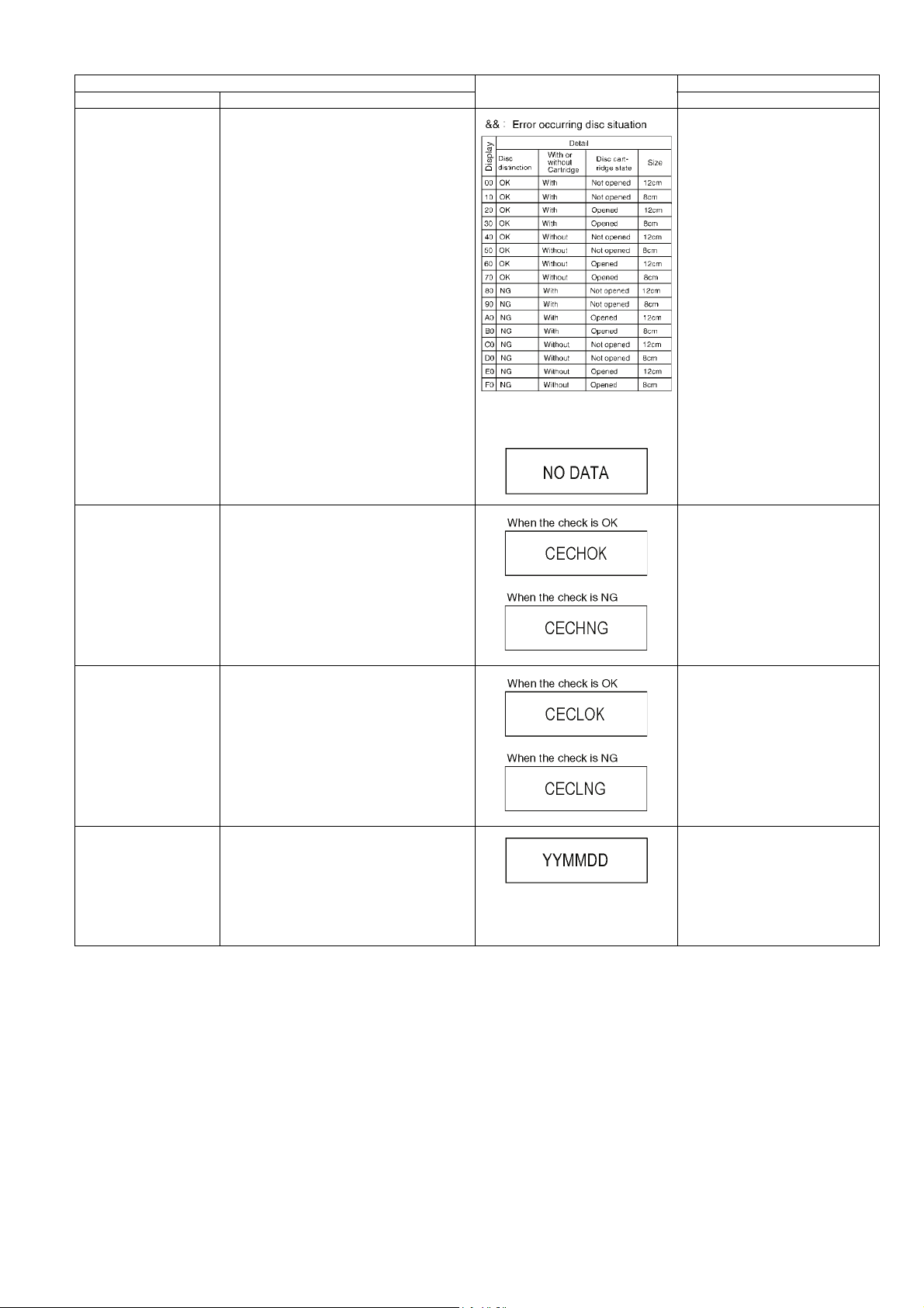
Item LCD display Key operation
Mode name Description (Remote controller key)
8. When the last error doesn't exist .
CEC (H) output check Check of the CEC terminal high output of
HDMI.
CEC (L) output check Check of the CEC terminal low output of
HDMI.
Manufacturing Date Read out the manufacturing date of the unit.
Press [5] [5] in service mode.
Press [5] [6] in service mode.
Press[6][1]in service mode.
YY: Year
MM: Month
DD: Day
19
Page 20
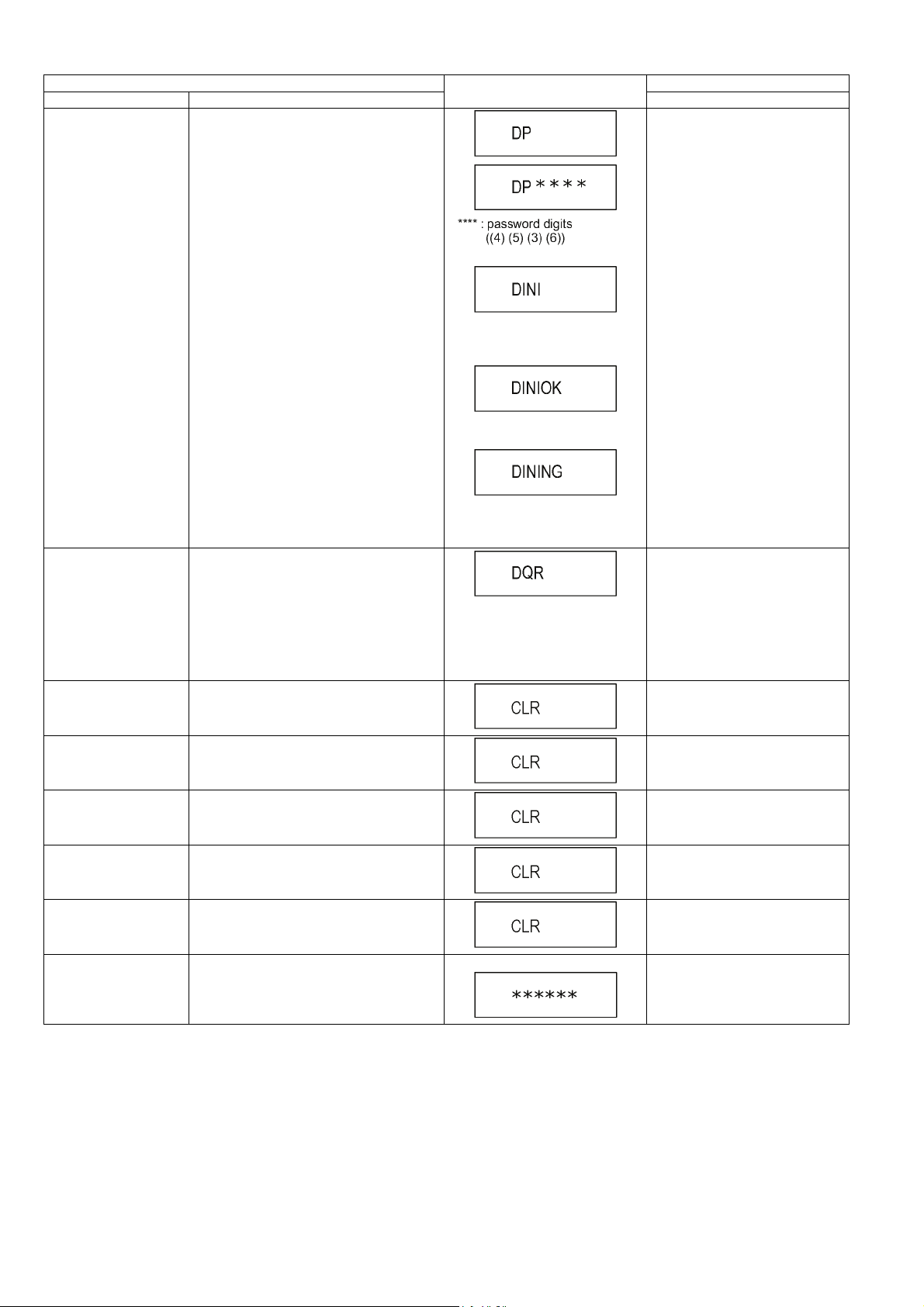
Item LCD display Key operation
Mode name Description (Remote controller key)
Drive adjustment value
initialization
Drive OPU-QR code
write
Initialize the drive going to factory production
adjustment values.
Initializing:
Successful adjustment value initialization and automatic adjustment
time :
Failed at initialization and automatic adjustment adjustment :
When you enter the wrong
password service mode initially
(SERV __ __) to return.
How to write drive OPU-QR code
Press[7][1]in service mode.
Wirte remote control number key
perform the initialization.
Press[7][2]in service mode.
Delete the Laser Used
Time
Delete the Last Drive
Error
Delete the Error History Error History information stored on the unit is
Initialization of Error code Last Error Code information stored by timer is
Initialization of the
Service Mode
Release Service Mode Release Service Mode and turns the Power
Laser used time information stored in the
memory of the unit is deleted.
Laser Drive Error information stored on the
BD Drive is deleted.
deleted.
deleted. (Write in F00)
Last Drive Error, Error History and Error code
information stored on the unit are initialized to
factory setting.
Off.
* Details are described in "Adjustment Instruction when Exchange
the OPU Ass'y or Main P.C.B.
adjustment value initialization
adjust".
Press [9] [5] in service mode.
Press [9] [6] in service mode.
Press [9] [7] in service mode.
Press [9] [8] in service mode.
Press [9] [9] in service mode.
Display in STOP (SS) mode. Press [POWER] button on the front
panel or Remote controller in service mode.
20
Page 21
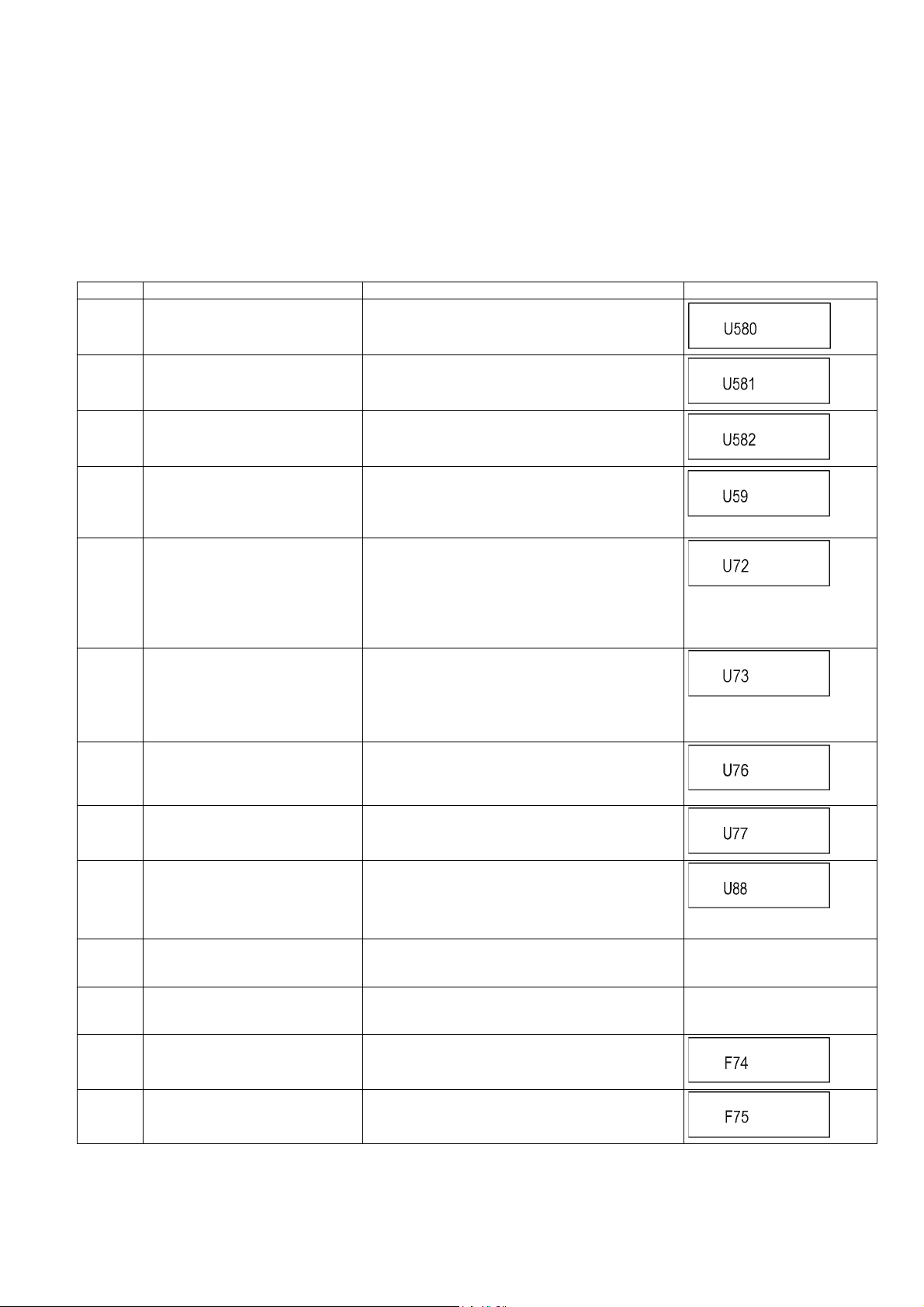
7 Troubleshooting Guide
7.1. Self-Diagnosis Functions
Self-Diagnosis Function provides information for errors to service personnel by “Self-Diagnosis Display” when any error has
occurred.
U** and F** are stored in memory and held.
You can check latest error code by transmitting [0] [1] of Remote Controller in Service Mode.
In case of clear the self-diagnosis display, remove the battery pack and the AC adaptor from the main unit after the power of the
main unit is turned off.
Error Code Diagnosis contents Description LCD Display
U580 Battery supply current abnormality A problem has occurred with the battery pack. Consult
U581 Abnormal charge time on battery power The battery pack has been recharging but has failed to
your dealer.
recharge for some reason. Recharge again.
U582 Battery-powered temperature anomaly You are recharging in a location that is too hot or too cold.
U59 Abnormal inner temperature detected Display appears when drive temperature exceeds 70°C.
U72 HDMI connection error
(communication error)
U73 HDMI connection error
(authentication error)
U76 Connection error This error is displayed when equipment such as TVs or
U77 Illegal disc error This error is displayed when it becomes impossible to
U88 Restoration is operation.
(When the disc is in the disc tray)
F00 No error information Initial setting for error code in memory
F58 Drive hardware error When drive unit error is detected, the event is saved in
F74 HDMI Device Key Communication
error
Recharge at normal temperature [+5 to +35 °C (+41 to
+95 °F)].
The power is turned off forcibly.
For 30 minutes after this, all key entries are disabled.
The event is saved in memory as well.
This error is displayed when there are any communication
problems with the unit and the equipments (TV, amplifier
etc.) connected to the unit by HDMI. (or when there is a
problem with the HDMI cable).
The display disappears only when the connection is
released. Neither the button operation nor the passage of
the fixed time disappear the display.
When authentication error occurs while the equipments
(TV, amplifier etc.) are connected by HDMI. (or when
there is a problem with the HDMI cable).
The display disappears only when the connection is
released. Neither the button operation nor the passage of
the fixed time disappear the display.
amplifiers connected to the unit with the HDMI cable do
not correspond to the copyright protection. (The BD/DVD
video where the copyright is protected cannot be played.)
reproduce because of copyright illegal information.
This error is displayed when there is a disc in the disc tray
or abnormality is confirmed during playback. It is shown
that the restoration to return the main unit operation
normally is operating. It becomes possible to use as soon
as not the breakdown but the U88 display disappears.
(Error code Initialization is possible with error code initialization and main unit initialization.)
memory.
This error is displayed when the information error is
occurred at HDMI device key loading.
"U59" is displayed for 30 minutes.
Display for 30 seconds.
Not automatic display. Press [0][1]
in service mode. (Remote controller key)
Not automatic display. Press [0][1]
in service mode. (Remote controller key)
F75 HDMI Device Key Loading error This error is displayed when the key of loaded is illegal at
HDMI device key loading.
21
Page 22
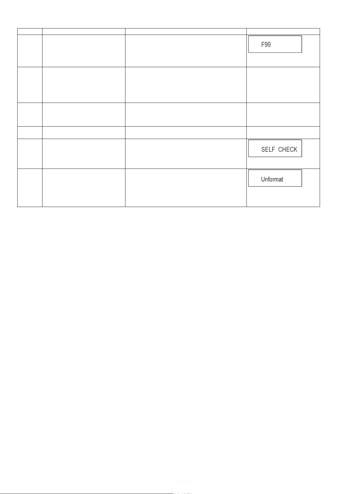
Error Code Diagnosis contents Description LCD Display
F99 Hang-up Displayed when communication error has occurred
between Main microprocessor and Timer microprocessor.
"F99" is displayed utill the [Power]
key is pressed.
UNSUPPORT
No Read Disc read error This error is displayed when the following are detected.
Hard Error Drive error This error is displayed when the drive detected a hard
Self Check Restoration operation This error is displayed when the restoration is operating
Unformat Unformatted disc error This error is displayed when the unformatted DVD-RAM/
Unsupported disc error This error is displayed when the following are detected.
1. When the unsupported format disc is reproduced.
2. When the unsupported format data is saved in the
supported format disc.
3. When it becomes impossible to read because the
quality of the disc is bad.
1.When the disc is dirty or damaged.
2. When falling in reading the reack information.
3. When the drive error occurs.
error.
because it is power failures or turns off power during a
operation. If there is no problem, the display disappears
automatically. If a display does not disappear, there is the
possibility that defective Main P.C.B. / Drive unit.
DVD-RW or the DVD-RW recorded by another make of
recorder is inserted.
"This disc is incompatible."
Display for 5 seconds.
"Cannot read, please check the
disc."
Display for 5 seconds.
"DVD drive error."
Display for 5 seconds.
This disc is not formatted properly.
Format the disc in DISC
MANAGEMENT?
22
Page 23
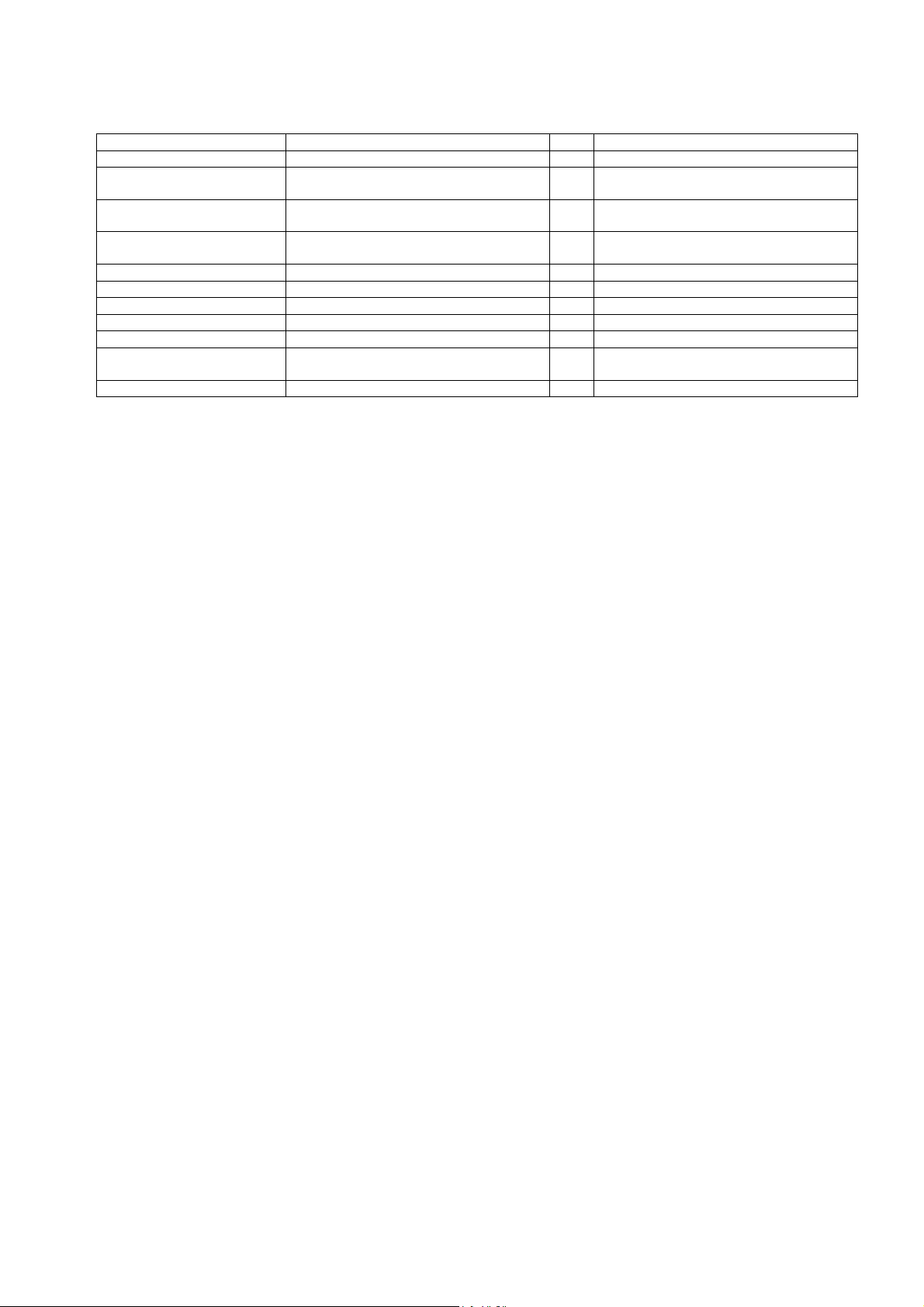
8 Service Fixture & Tools
Part No. Uses Pcs Interchangeability with Old Fixture Tools
----- New CD-R disc 1
RFKZ0558(5Pin)+ RFKZ0559 Extension cable + connector
(Traverse Unit-Main P.C.B.)
RFKZ0560(8Pin) + RFKZ0561 Extension cable + connector
(Traverse Unit-Main P.C.B.)
RFKZ0562(6Pin)+ RFKZ0563 Extension cable + P.C.B.
(PC-Main P.C.B. (P51601)
RFKZ0139 Serial Cable (PC-Main P.C.B. (P51601)/6pin) 1 Same as B100 series
RFKZ03D01KS Lead Free Solder (0.3mm/100g Reel) Sharing with EH55/EH75V/XP10/XW30 Series
RFKZ06D01KS Lead Free Solder (0.6mm/100g Reel) Sharing with EH55/EH75V/XP10/XW30 Series
RFKZ10D01KS Lead Free Solder (1.0mm/100g Reel) Sharing with EH55/EH75V/XP10/XW30 Series
RFKZ0316 Lead Free Solder with Low Melting Point
for Unsolder (50g)
RFKZ0328 Flux Sharing with EH55/EH75V/XP10/XW30 Series
1 Same as B100 series
1 Same as B100 series
1 Same as B100 series
Sharing with EH55/EH75V/XP10/XW30 Series
23
Page 24
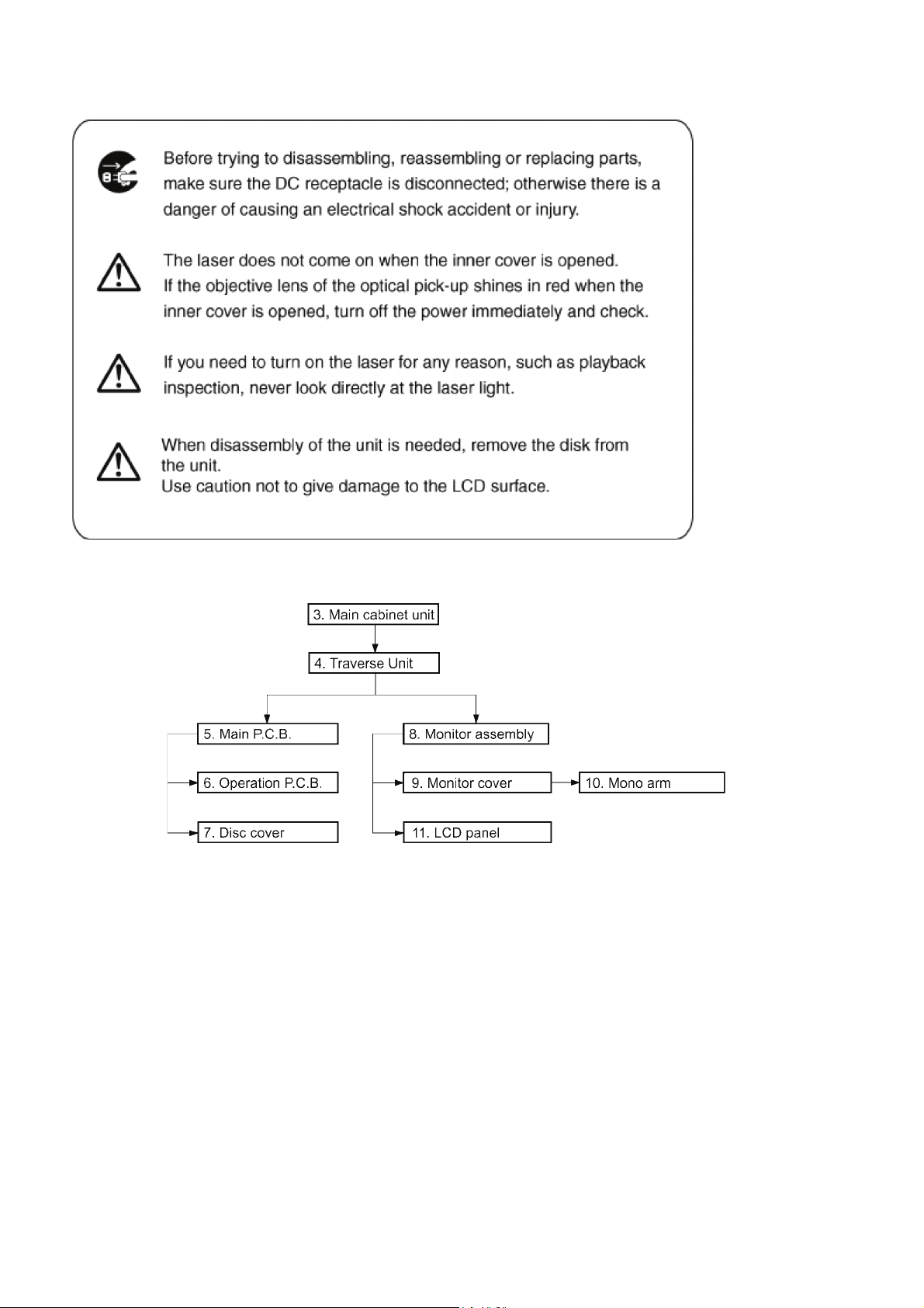
9 Disassembly and Assembly Instructions
9.1. Disassembly Flow Chart
24
Page 25
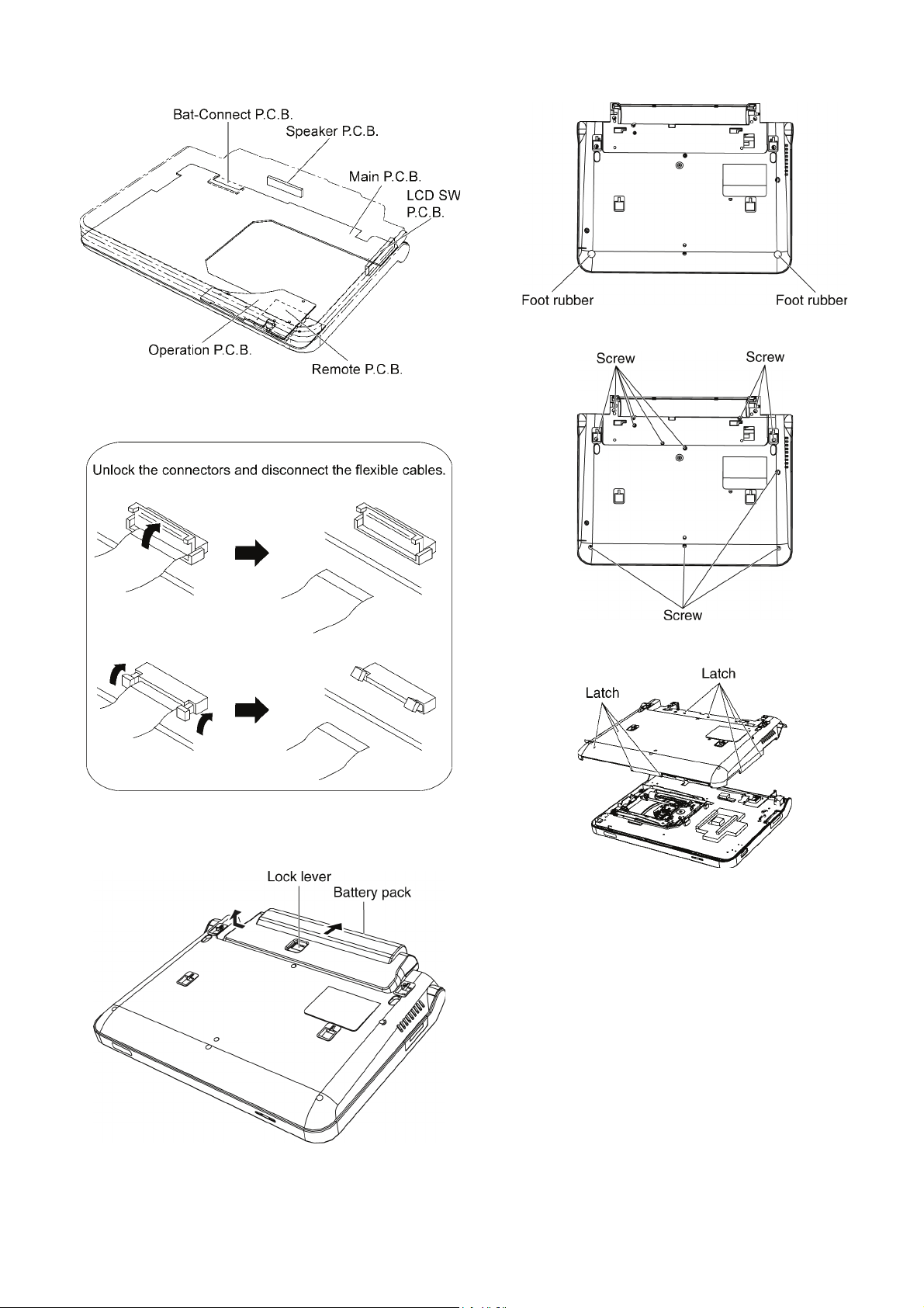
9.2. P.C.B. location
9.3. Main cabinet unit
1. Remove the 2 foot rubbers.
2. Remove the 13 screws .
<Removing battery pack>
Release the lock lever and remove the battery pack in the
direction of the arrow.
3. Release the latches and remove the bottom cabinet.
25
Page 26
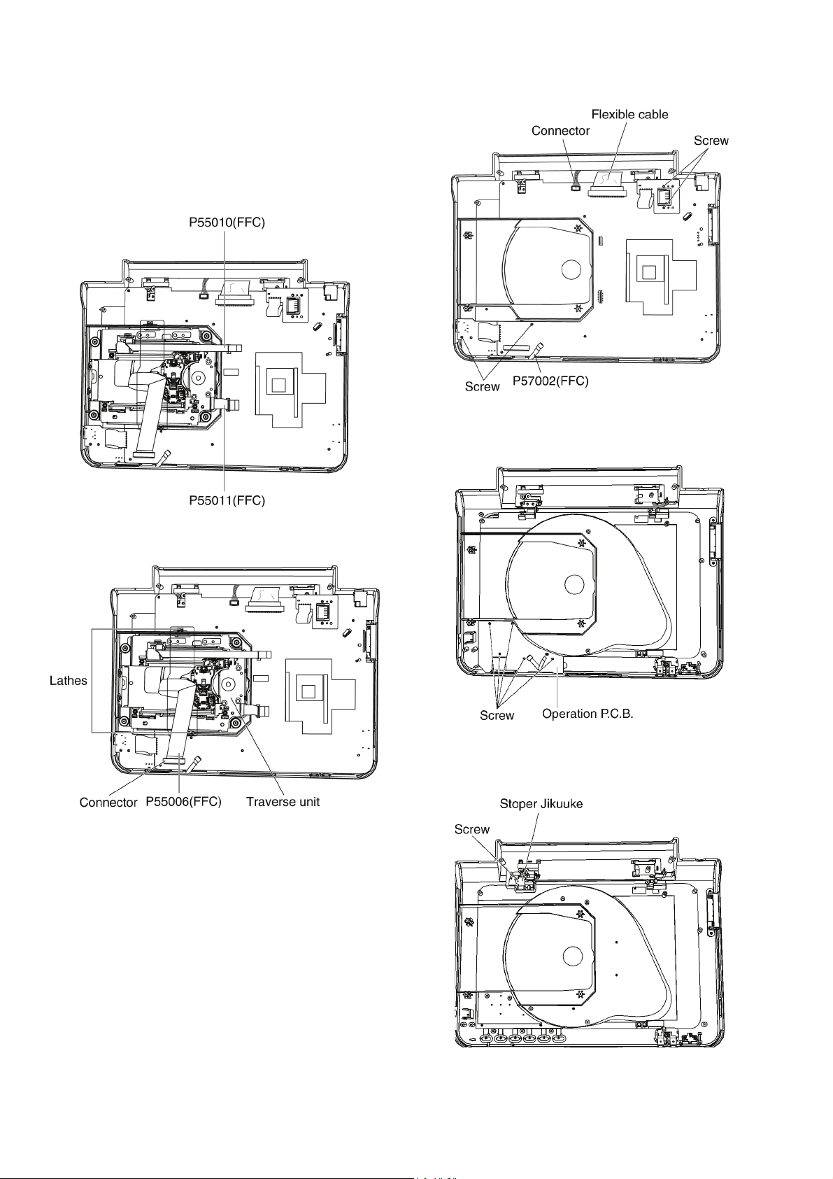
9.4. Traverse Unit
NOTE:
The countermeasure against static electricity is necessary
when servicing the surrounding of traverse unit.
Moreover, the traverse unit is the precision optical part.
Take care not to touch surrounding of the lens and not to
shock to the traverse unit.
1. Pull out the P55010(FFC) and the P55011(FFC).
3. Remove the 4 screws and remove the main P.C.B. with
BAT-CONNECTOR P.C.B. and HP P.C.B..
9.6. Operation P.C.B.
1. Remove the 5 screws and remove the Operation P.C.B..
2. Release the connector and latches, pull out the
P55006 (FFC), and then remove the traverse unit.
9.5. Main P.C.B.
1. Remove the connector and the flexible cable.
2. Pull out the P57002(FFC).
9.7. Disc cover
1. Remove the screw and the STOPER JIKUUKE.
26
Page 27
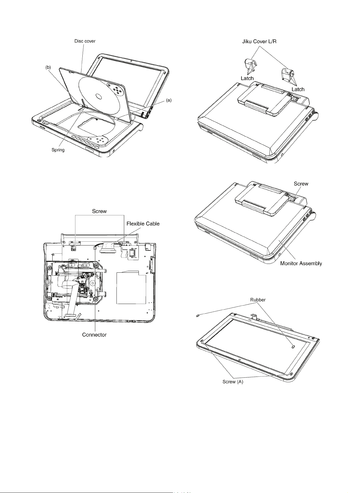
2. Remove the disc cover in order of (a) and (b).
Caution:
Please don't lose the spring.
9.8. Monitor assembly
1. Remove the connector and the flexible cable.
2. Remove the 2 screws.
3. Release the latches and remove the JIKU COVER L/R.
4. Remove the screw and remove the monitor assembly.
9.9. Monitor cover
1. Remove the 2 rubbers and the 2 screws (A).
27
Page 28
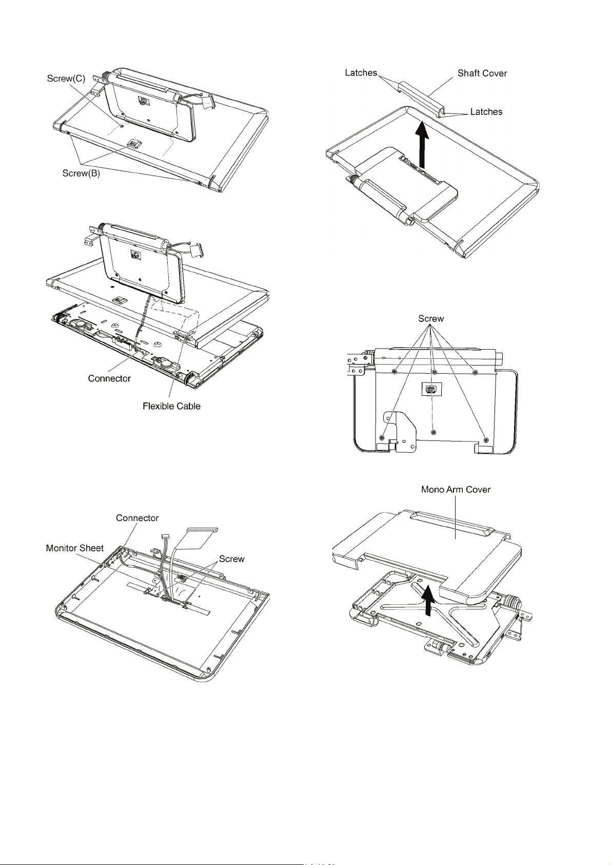
2. Remove the 3 screws (B) and screw (C).
3. Remove the connector and the flexible cable.
2. Release the latches and remove the shaft cover.
3. Release the friction hinge from boss and remove the
mono arm assembly.
4. Remove the 6 screws.
4. Remove the monitor cover.
Caution to be taken when installing monitor cover
Please do not nip the wire.
9.10. Mono arm
1. Remove the connector and 2 screws, then remove the
monitor sheet.
5. Release the latches and remove the mono arm cover.
28
Page 29
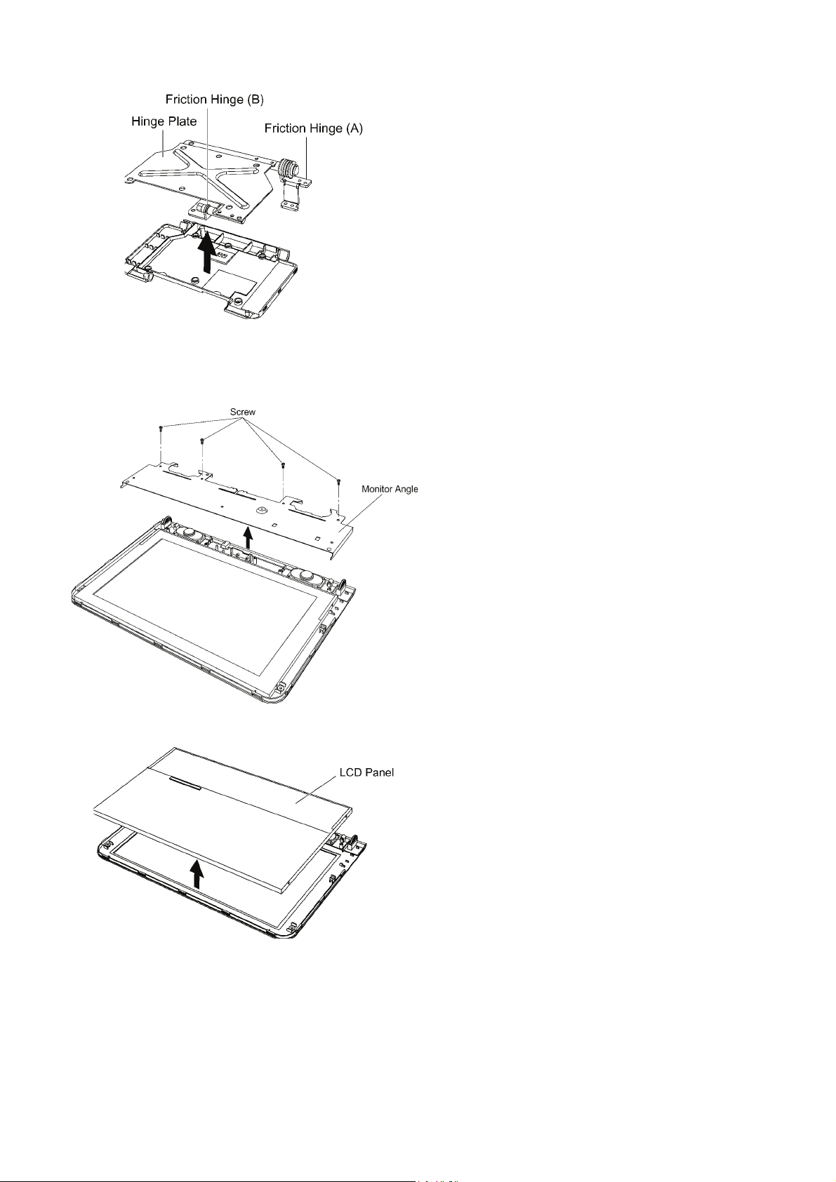
6. Remove the plate and friction hinge (A)/(B).
9.11. LCD panel
1. Remove the 4 screws.
2. Remove the monitor angle.
3. Remove the LCD panel.
29
Page 30
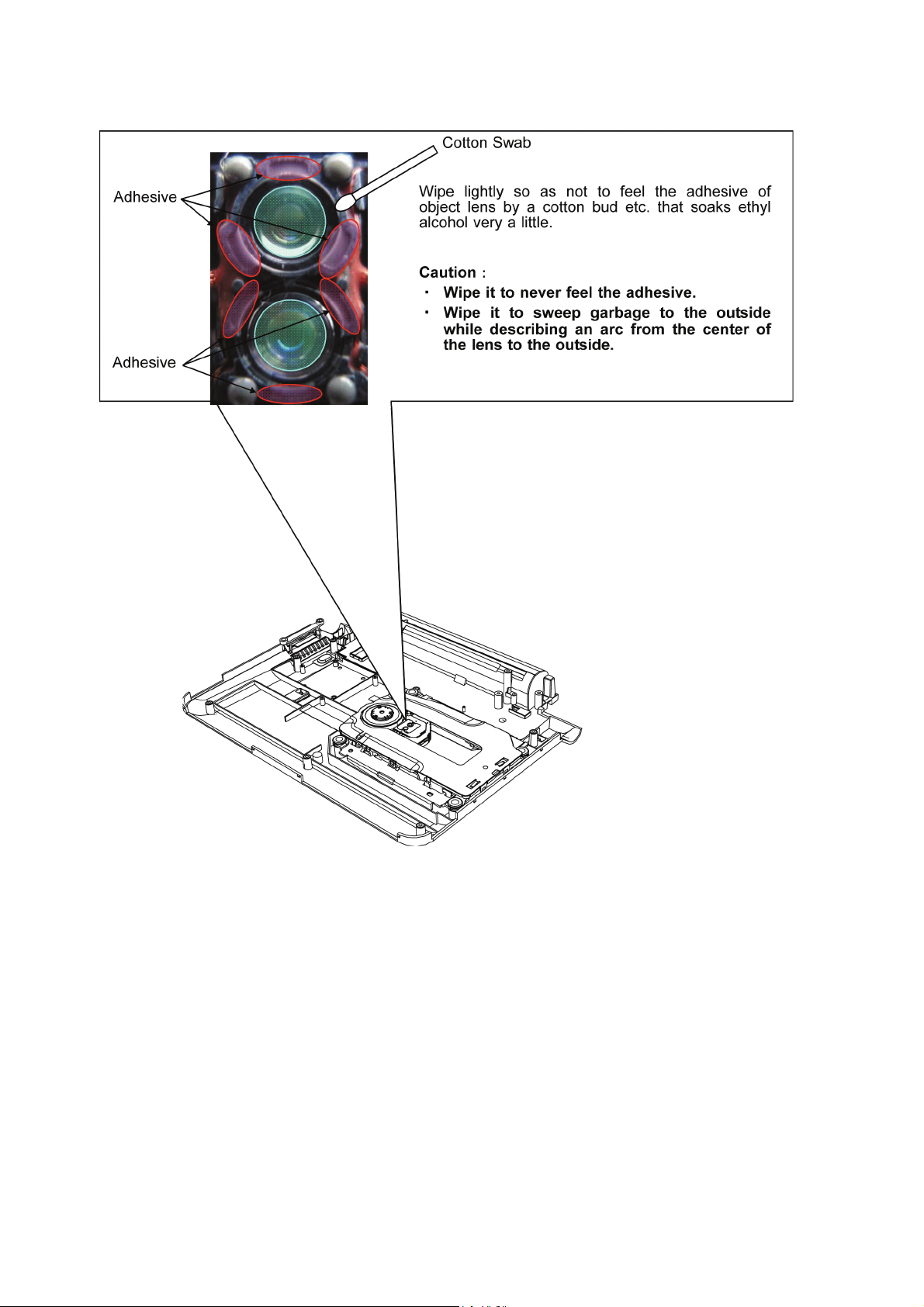
9.12. Cleaning of the Optical Pick-up
Disassemble to the item 4 (9.3. MAIN CABINET UNIT), and clean the optical pick-up.
30
Page 31
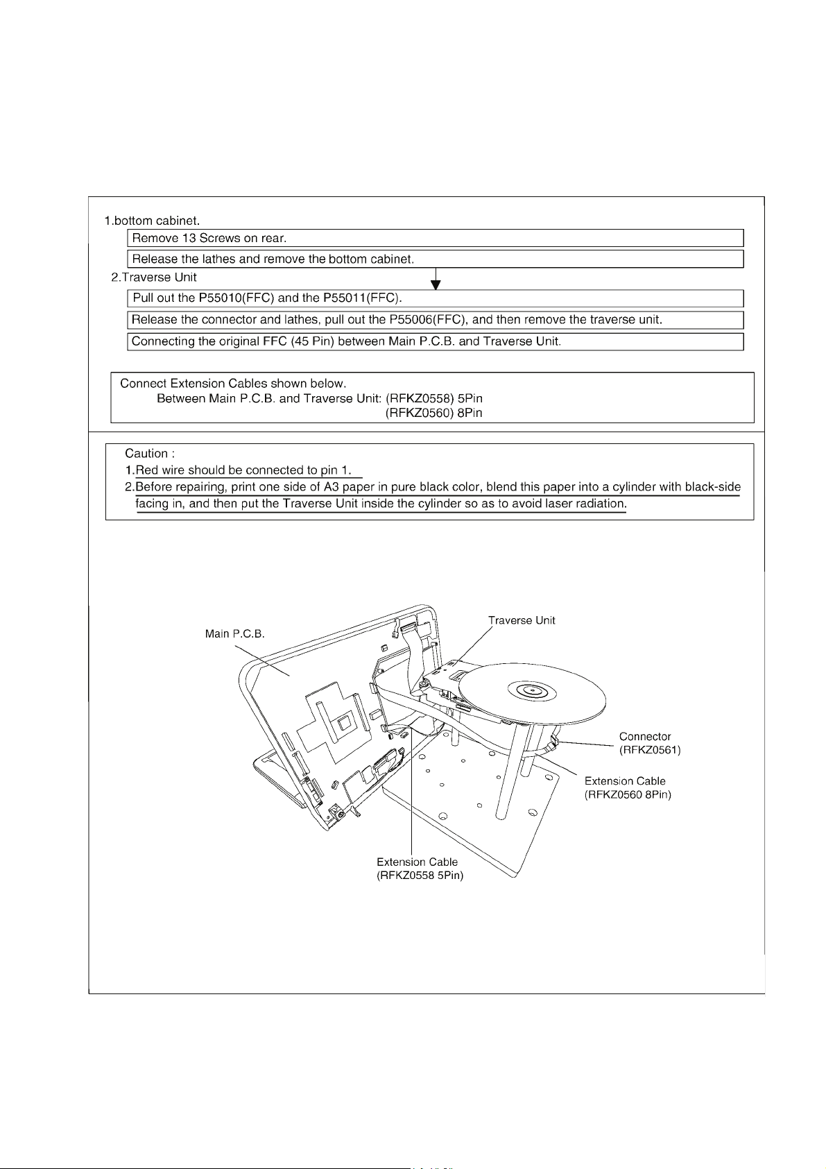
10 Measurements and Adjustments
10.1. Service Positions
Note:
For description of the disassembling procedure, see the section 9.
10.1.1. Checking and Repairing of Main P.C.B. (1)
31
Page 32
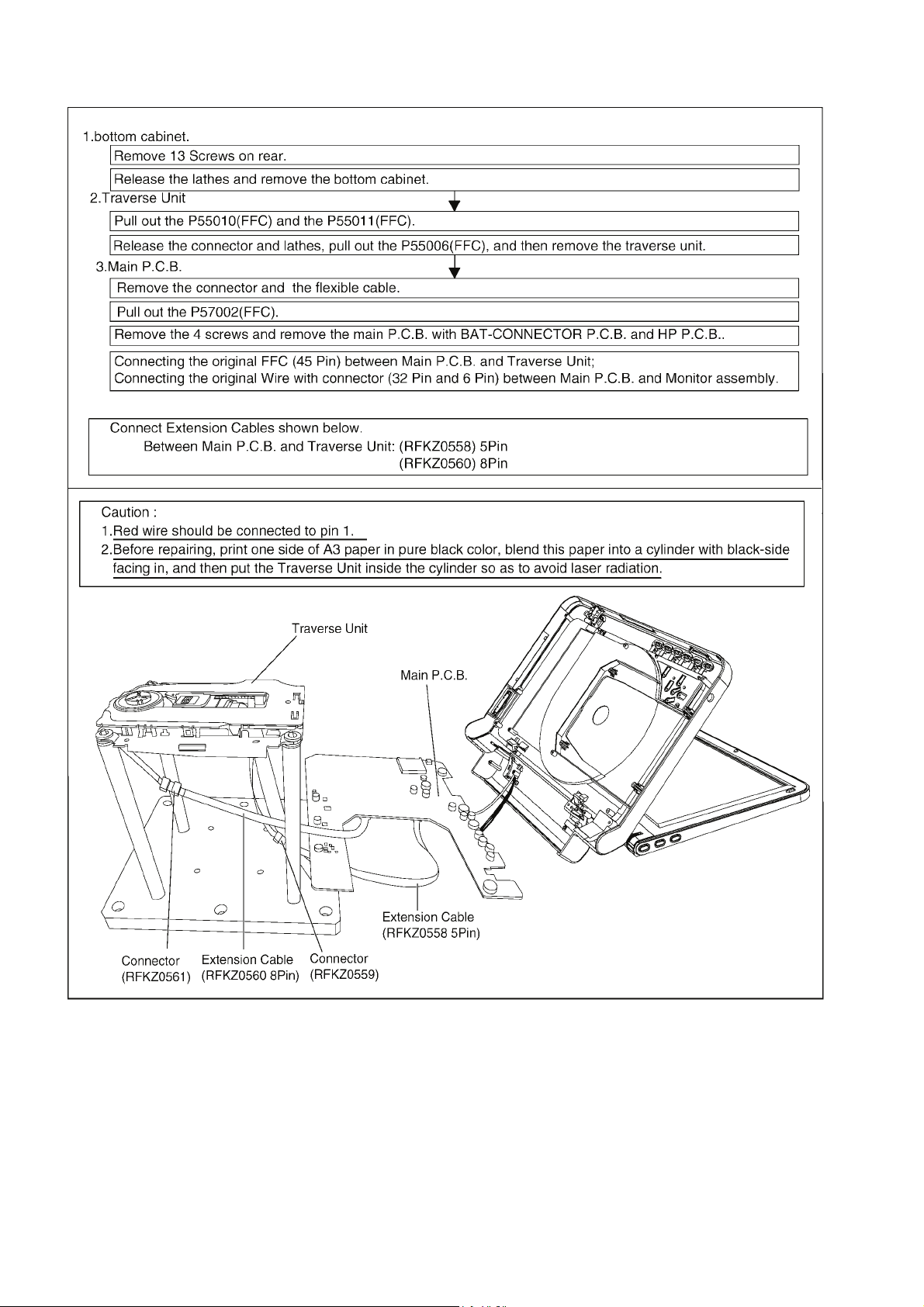
10.1.2. Checking and Repairing of Main P.C.B. (2)
32
Page 33
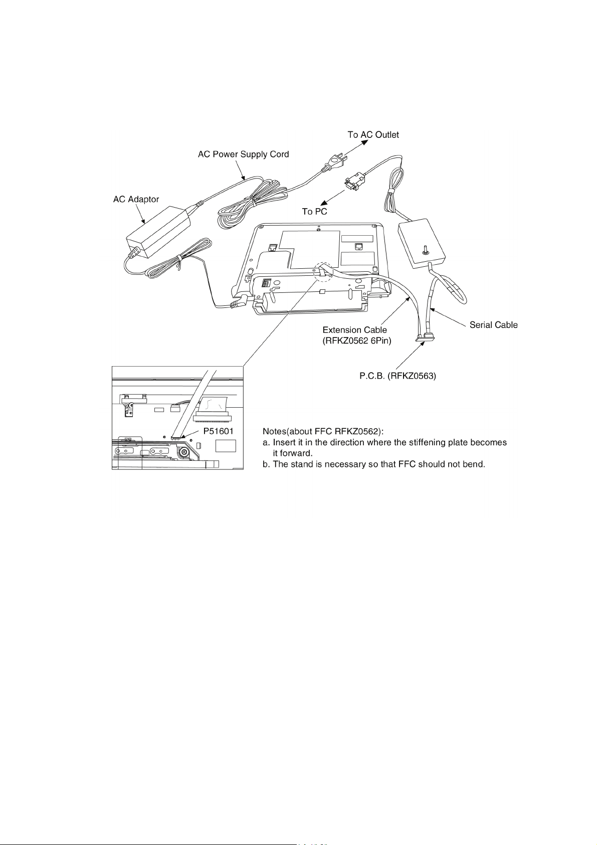
10.1.3. Adjustment Value Initialization Adjustment when exchange the Traverse or Main P.C.B.
Refer to “9. Disassembly and Assembly Instructions” for details of disassembly and assembly.
10.3. Adjustment Instruction when Exchange the Traverse or Main P.C.B. (Adjustment Value Initialization Adjustment)
1. Connect the serial cable (RFKZ0139) to the main P.C.B. (P51601).
2. Fix the traverse unit from the bottom with thirteen screws.
33
Page 34
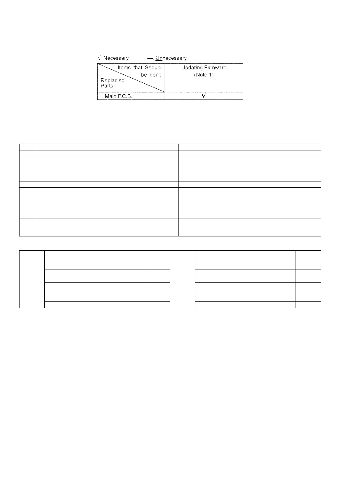
10.2. Caution for Replacing Parts
10.2.1. Items that should be done after replacing parts
Note 1:
Download latest Firmware and burn it on CD-R or CD-RW, and update Firmware.
10.2.2. Standard Inspection Specifications after Making Repairs
After making repairs, we recommend performing the following inspection, to check normal operation.
No. Procedure Item to Check
1 Turn on the power, and confirm items pointed out. Items pointed out should reappear.
2 Insert RAM disc. The Panasonic RAM disc should be recognized.
4 Perform playback for one minute using the RAM disc. No abnormality should be seen in the picture, sound or operation.
5 Perform playback for one minute using the BD-Video disc. No abnormality should be seen in the picture, sound or operation.
6 If a problem is caused by a BD-Video disc, VCD, DVD-R,
DVD-Video, Audio-CD, or MP3, playback the test disc.
7 After checking and making repairs, upgrade the firmware to the
latest version.
8 Transfer [9][9] in the service mode setting, and initialize the service
settings (return various settings and error information to their
default values. The laser time is not included in this initialization).
Use the following checklist to establish the judgement criteria for the picture and sound.
*Panasonic DVD-RAM disc should be used when recording and
playback.
No abnormality should be seen in the picture, sound or operation.
Make sure that [UPD OK] appears in the FL displays.
*[UNSUPPORT] display means the unit is already updated to
newest same version. Then version up is not necessary.
Make sure that [CLR] appears in the FL display.
After checking it, turn the power off.
Item Contents Check Item Contents Check
Picture
Block noise
Crosscut noise Noise (static, background noise, etc.)
Dot noise The sound level is too low.
Picture disruption The sound level is too high.
Not bright enough The sound level changes.
Too bright
Flickering colour
Colour fading
Sound
Distorted sound
34
Page 35
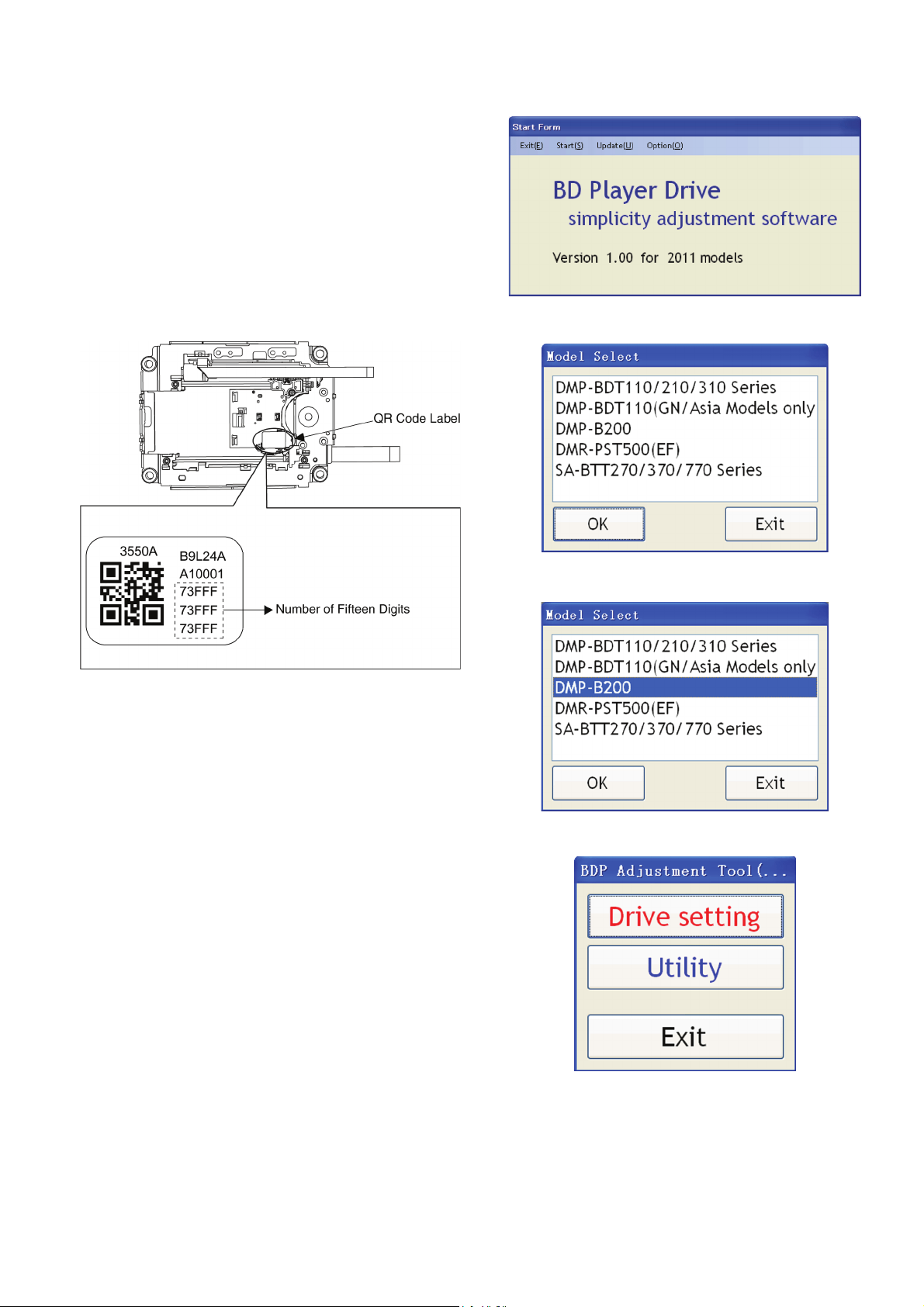
10.3. Adjustment Instruction when Exchange the OPU Ass'y or Main P.C.B. adjustment value initialization adjust
(Preparation)
1. Install adjustment software "BD Player Drive adjustment
Software Ver 1.0" of the pertinent model placed in the
"TSN Website", therefore, access to "TSN Website" at
"Support Information from NWBG/VDBG-AVC".
2. Take notes of the number of fifteen digits of QR code
label (label of the lower) pasted to bottom of the OPTICAL
PICK-UP.
(Adjustment Procedure)
1. Start the “BDPSimpleAdj” software.
2. Start "BDP Adjustment", and click the Start button.
3. Prepare a new CD-R disc, and then make the disc for the
upgrade of the latest firmware.
[Upgrade procedure of firmware by disk making]
•Step 1.
Choose the model that you are using and download the firmware.
•Step 2.
Please defrost the downloaded file.
•Step 3.
Prepare a CD-R disc, and write the above-mentioned file on
the CD-R disc, and then make the disc for the upgrade.
•Step 4.
Set the disc the made upgrade, and do the upgrade of the
firmware.
3. Select “DMP-B200”.
Select “OK”.
35
Page 36
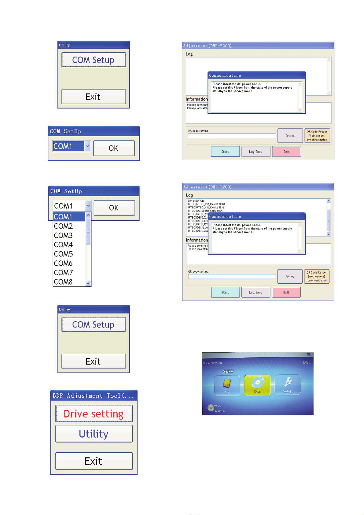
4. Select “Utility”.
5. Select “COM Setup”.
8. Select “Drive setting”.
6. According to computer interfaces to select. For example,
select "COM1".
Select “OK”.
9. Connect the AC power supply code with the power supply
outlet.
10. Turn off the power, press [5], [9] and [Red] keys for a long
time. [70 RET] will be dispalyed, then press [Right] button, [80 SRV] will be displayed, press [OK] button, or
press the combination of the keys [SUBMENU], [PLAY]
and [VOL DOWN] on the device directly.
LCD display of B200 shows as below.
7. Select “Exit”.
36
Page 37
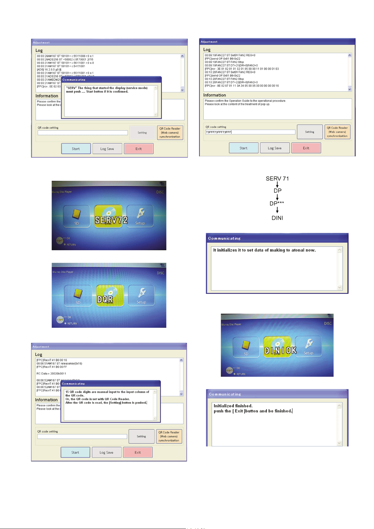
Computer screen displays as below.
12. Please manually enter 15 digits QR code.
11. Press the Start button, and LCD of B200 shows in
sequence as follows:
Simultaneously, the following computer screen shows:
13. Press the Setting button, and LCD of B200 shows in
sequence as follows.
Computer screen displays as below.
LCD display of B200 with the adjustment value initialization finished.
Computer screen displays as below.
14. Cut the power off, detach the serial cable (RFKZ0139),
and assemble the main body, and then confirm the sound
with CD-ROM test disc (RFKZ0516).
15. Improve the version to the latest firmware, after traverse
unit or main P.C.B. is exchanged.
37
Page 38
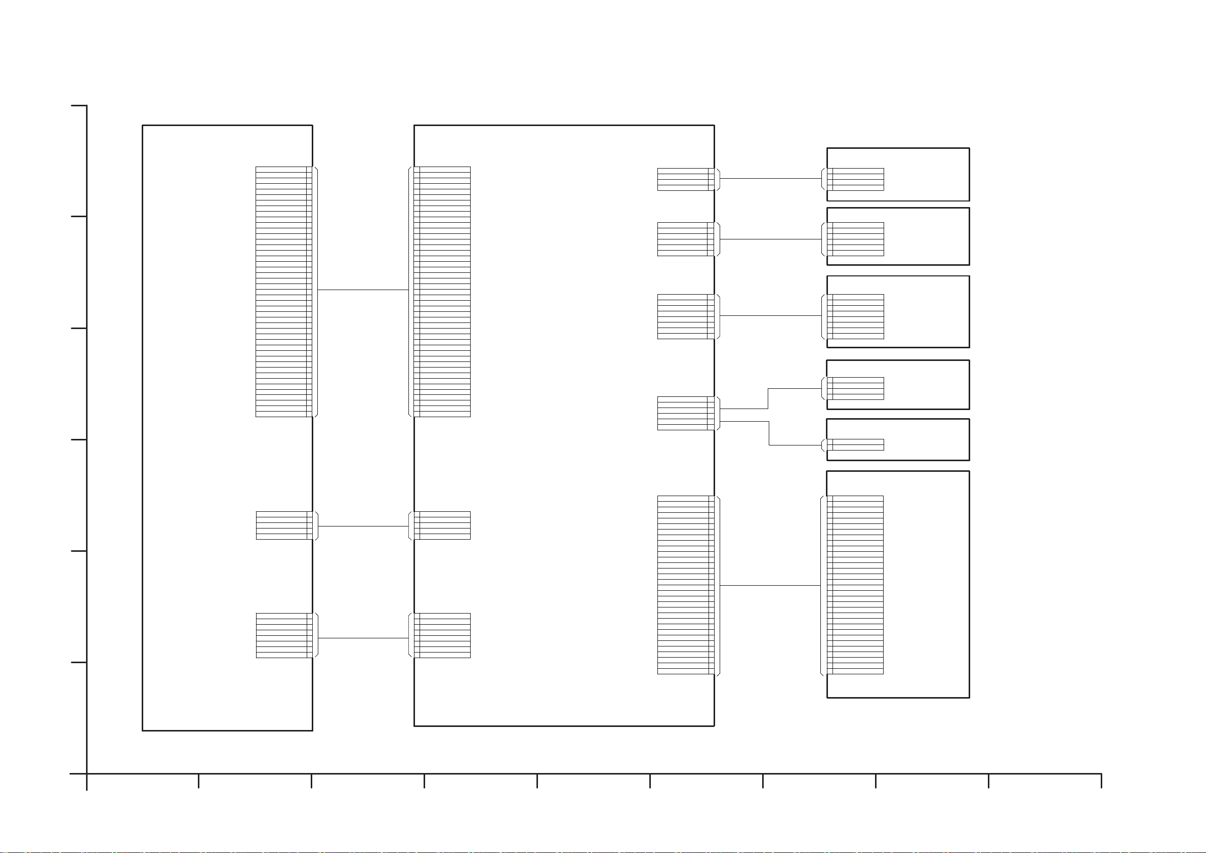
11 Schematic Diagram
11.1. Interconnection Schematic Diagram
E
D
F
CL-ACT FOC2+
CL-ACT FOC2-
CL-ACT TRK-
CL-ACT TRK+
CL-ACT FOC1+
CL-ACT FOC1-
CL-ACT SB+
CL-ACT SBCL-ACT SACL-ACT SA+
LDD GND
LDD GND
TMP
LDD GND
LDD BVCC
LDD GND
LDD MON
LDD GND
LDMKR
LDD VCC
LDD GND
LDD LDON
LDD SDIO
LDD SCLK
LDD SEN
LDD GND
PDIC VCC
PDIC GND
PDIC C/A2
PDIC D/A4
PDIC SW2
PDIC SW1
PDIC A/A3
PDIC B/A1
PDIC GND
PDIC RFN
PDIC GND
PDIC RFP
PDIC GND
PDIC FJ/B3
PDIC GK/B1
PDIC E1/B6
PDIC HL/B5
PDIC GND
PDIC VREF
1
2
3
4
5
6
7
8
9
10
11
12
13
14
15
16
17
18
19
20
21
22
23
24
25
26
27
28
29
30
31
32
33
34
35
36
37
38
39
40
41
42
43
44
45
P55006
CL-ACT FOC2+
1
CL-ACT FOC2-
2
CL-ACT TRK-
3
CL-ACT TRK+
4
CL-ACT FOC1+
5
CL-ACT FOC1-
6
CL-ACT SB+
7
8
9
CL-ACT SA+
10
11
12
13
14
15
16
17
18
19
20
21
22
23
24
25
26
27
28
29
30
31
32
33
34
35
36
37
38
39
40
41
42
43
44
45
CL-ACT SBCL-ACT SA-
LDD GND
LDD GND
TMP
LDD GND
LDD BVCC
LDD GND
LDD MON
LDD GND
LDMKR
LDD VCC
LDD GND
LDD LDON
LDD SDIO
LDD SCLK
LDD SEN
LDD GND
PDIC VCC
PDIC GND
PDIC C/A2
PDIC D/A4
PDIC SW2
PDIC SW1
PDIC A/A3
PDIC B/A1
PDIC GND
PDIC RFN
PDIC GND
PDIC RFP
PDIC GND
PDIC FJ/B3
PDIC GK/B1
PDIC E1/B6
PDIC HL/B5
PDIC GND
PDIC VREF
KEY3
KEY21
KEY1
GND
BAT+
BAT+
BAT-T
D
GND
GND
HPOUTL
AGND
HPOUTR
MUTE
HPJIN-L
DGND
REMOCON
PW_3.3VR
SPL+
SPLSPR+
SPRGND
KEY2
P57002
PJ1401
PJ4001
P4002
1
2
3
4
1
2
3
4
5
6
1
2
3
4
5
6
7
8
6
5
4
3
2
1
MAIN_SW P.C.B.
P6101
KEY3
1
KEY21
2
KEY1
3
GND
4
BAT-CONNECTOR P.C.B.
1
BAT+
BAT+
2
BAT-T
3
D
4
GND
5
GND
6
HP_REMOCON P.C.B.
HPOUTL
1
AGND
2
HPOUTR
3
MUTE
4
HPJIN-L
5
DGND
6
REMOCON
7
PW_3.3VR
8
SPEAKER P.C.B.
P6201
4
SPL+
3
SPLSPR+
2
SPR-
1
LCD_SW P.C.B.
P6001
GND
2
KEY2
1
C
B
A
BD DRIVE
P55010
1
A-
2
B-
3
B+
4
A+
NC(GND) NC(GND)
GND
VH+
VH-
5
1
W
2
V
3
U
4
5
6
U+
7
U-
8
1
2
3
4
5
P55011
1
2
3
4
5
6
7
8
ABB+
A+
GND
W
V
U
VH+
U+
U-
VH-
MAIN P.C.B.
GND
NC/XR
NC/YU
NC/XL
NC/YD
VDD(LED)
VDD(LED)
VDD(LED)
AVSS
AVSS
NC
NC
AVSS
RXCLK+
RXCLK-
AVSS
RXIN2+
RXIN2-
AVSS
RXIN1+
RXIN1-
AVSS
RXIN0+
RXIN0-
NC
NC
ADJ
NC
VCC
VCC
AVSS
GND
FP8801
LCD PANEL
1
2
3
4
5
6
7
8
9
10
11
12
13
14
15
16
17
18
19
20
21
22
23
24
25
26
27
28
29
30
31
32
GND
1
NC/XR
2
NC/YU
3
NC/XL
4
NC/YD
5
VDD(LED)
6
VDD(LED)
7
VDD(LED)
8
AVSS
9
AVSS
10
NC
11
NC
12
13
AVSS
RXCLK+
14
RXCLK-
15
16
AVSS
17
RXIN2+
18
RXIN2-
19
AVSS
20
RXIN1+
21
RXIN1-
22
AVSS
23
RXIN0+
24
RXIN0-
25
NC
26
NC
27
ADJ
28
NC
29
VCC
30
VCC
31
AVSS
32
GND
DMP-B200EB/EE/EG
INTERCONNECTION
ISCHEMATIC DIAGRAM
1
98765432
38
Page 39
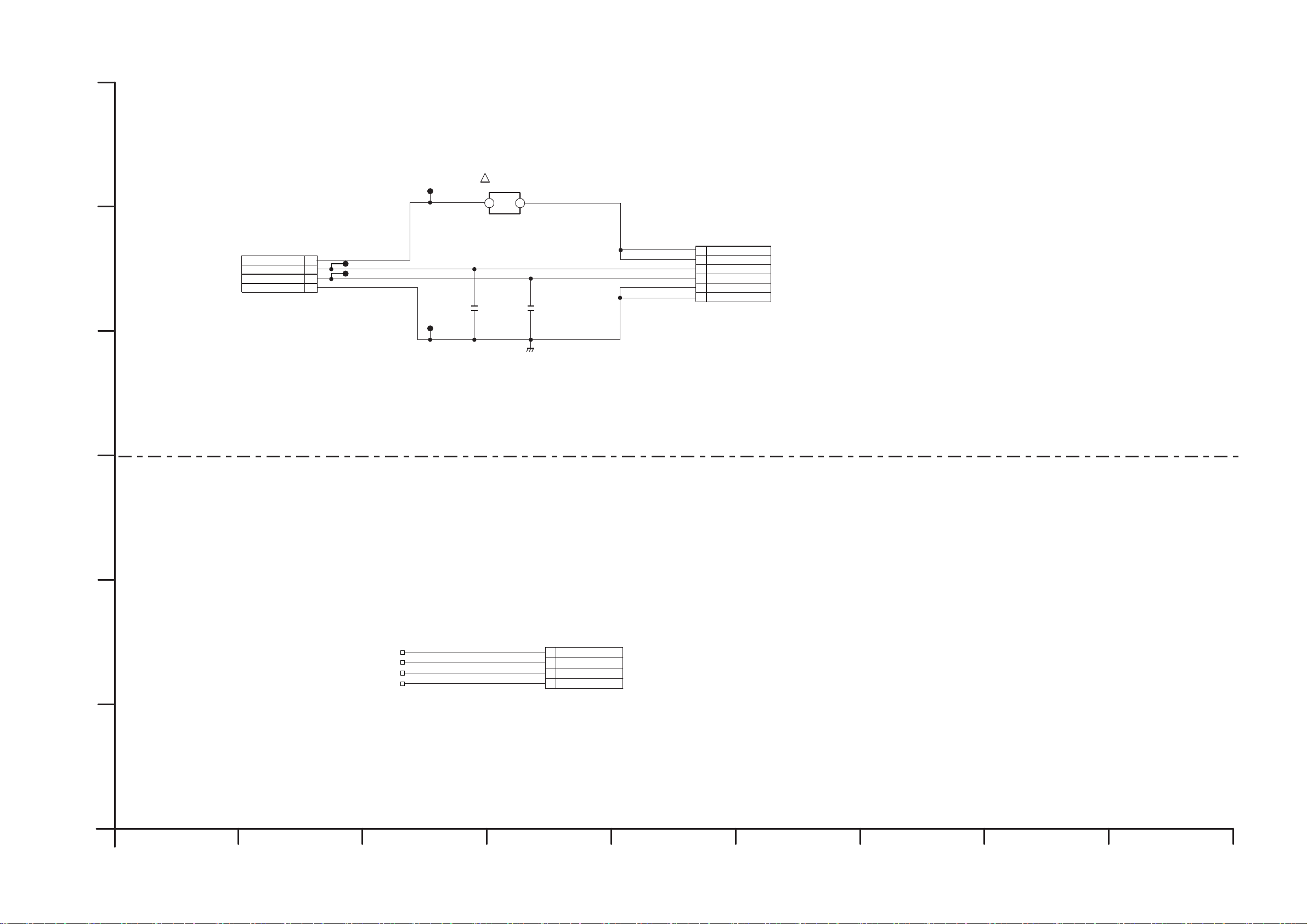
F
E
D
1
C
B
A
98765432
SCHEMATIC DIAGRAM
1
BAT+
BAT-T
D
GND
4
3
2
JK1801
G1C220KA0138
1
5
6
BAT+
BAT+
BAT-T
D
GND
GND
4
3
2
21
IP1801
D1JBR012A007
C1802
1000P
C1801
1000P
CL1801
CL1802
CL1804
CL1803
!
S_BAT_CONNECTOR
MAIN P.C.B.
TO PJ1401
S_SPEAKER SCHEMATIC DIAGRAM
SPLSPR+
SPL+
3
1
2
4
P6201
K1KA04AA0051
SPR-
TO P4002
MAIN P.C.B.
RL6201
RL6202
RL6203
RL6204
DMP-B200EB/EE/EG
DMP-B200EB/EE/EG
11.2. Bat-Connector and Speaker Schematic Diagram
39
Page 40
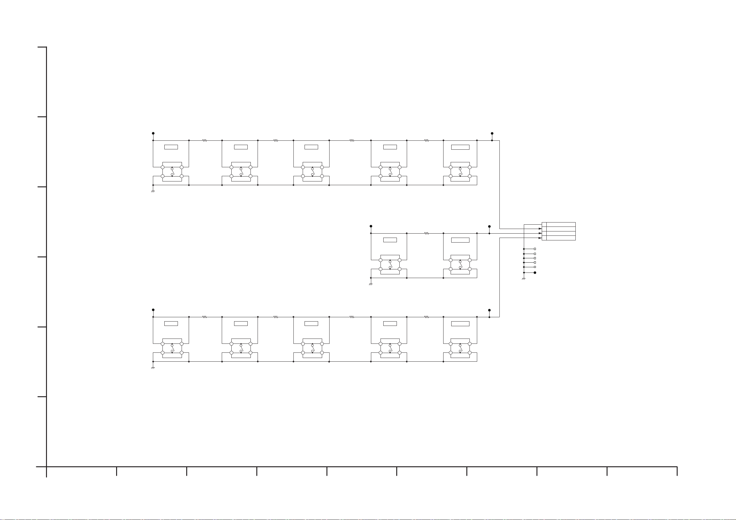
11.3. OPERATION Schematic Diagram
KEY1
KEY21
GND
3
1
2
4
P6101
K1MY04BA0041
KEY3
R6102
2.2K
R6103
3.3K
R6104
4.7K
S6101
K0F111A00472
R6101
1.5K
STOP
TO P57002
MAIN P.C.B.
AV SELECT
R_SKIPF_SKIP
PLAY
TL6102
F
E
D
1
C
B
A
98765432
S_MAIN_SW SCHEMATIC DIAGRAM
31
2 4
S6103
K0F111A00472
31
2 4
S6105
K0F111A00472
31
2 4
S6104
K0F111A00472
31
2 4
S6102
K0F111A00472
31
2 4
R6107
2.2K
R6108
3.3K
R6109
4.7K
S6108
K0F111A00472
R6106
1.5K
RETURN
SUB MENU
ENTERRIGHT
LEFT
TL6106
TL6105
31
2 4
S6110
K0F111A00472
31
2 4
S6112
K0F111A00472
31
2 4
S6111
K0F111A00472
31
2 4
S6109
K0F111A00472
31
2 4
S6106
K0F111A00472
R6105
3.3K
DOWN
UP
TL6104
TL6103
31
2 4
S6107
K0F111A00472
31
2 4
TL6101
RL6101
RL6102
RL6103
RL6104
RL6105
TL6107
DMP-B200EB/EE/EG
40
Page 41
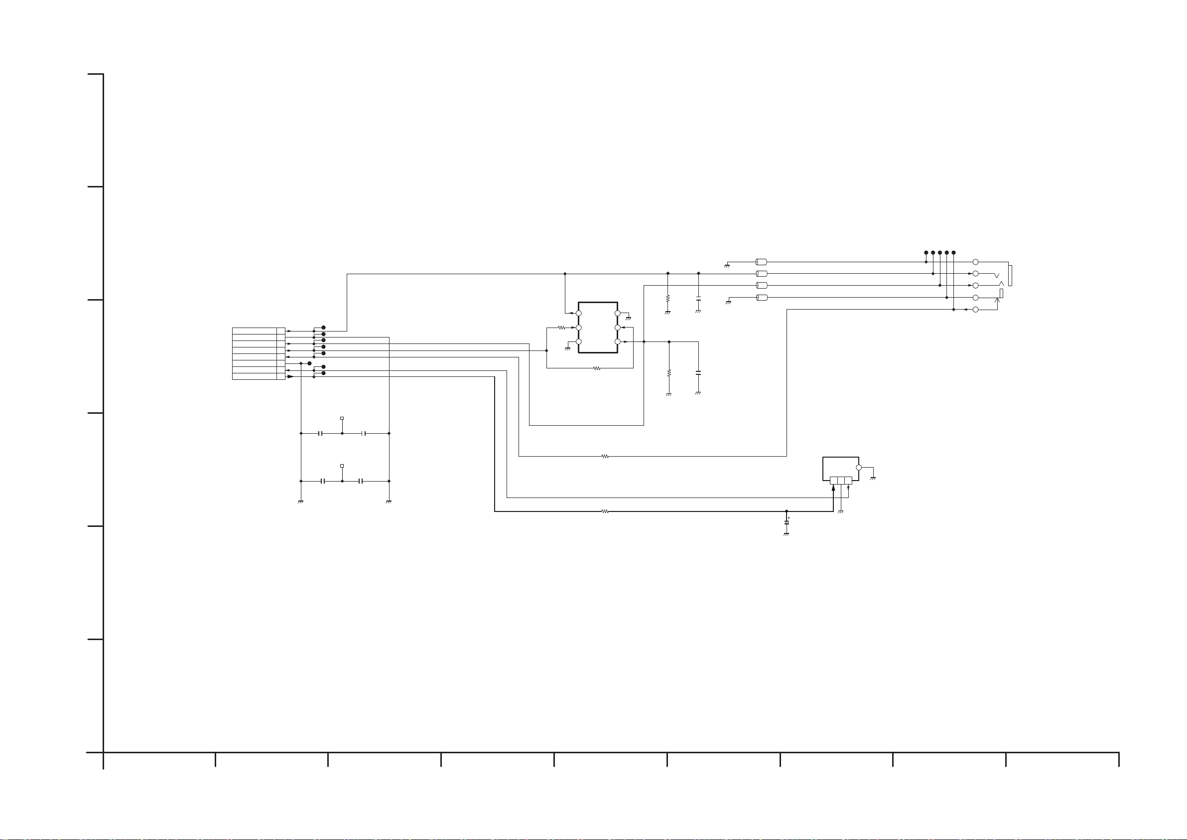
11.4. HP_REMOCON SCHEMATIC DIAGRAM
F
E
D
1
C
B
A
98765432
HP_REMOCON SCHEMATIC DIAGRAM
1
5
6
7
8
HPOUTL
AGND
HPOUTR
MUTE
HPJIN-L
DGND
REMOCOM
PW_3.3VR
4
3
2
TO PJ4001
MAIN P.C.B.
1E
2C
1B
1C
2E
2B
6
5
4
3
2
1
CL4131
CL4132
CL4129
CL4128
CL4127
QR4123
B1GFGCAA0001
R4133
4.7K
C4131
0.01
R4134
4.7K
C4132
0.01
LB4190
J0JBC0000028
LB4194 J0JBC0000028
LB4193 J0JBC0000028
LB4192
J0JBC0000028
JK4103
HP OUT
K2HC103B0213
1
2
3
4
5
R4135
560
R4136
560
R4137
1K
R4101
47
312
IR4101
6.3V 47
C4101
PNA4811M00YD
G1
C4104
100P
C4103
100P
RL4101
C4106
100P
C4105
100P
RL4102
CL4110
CL4111
CL4112
CL4113
CL4114
CL4116
CL4117
CL4115
DMP-B200EB/EE/EG
41
Page 42
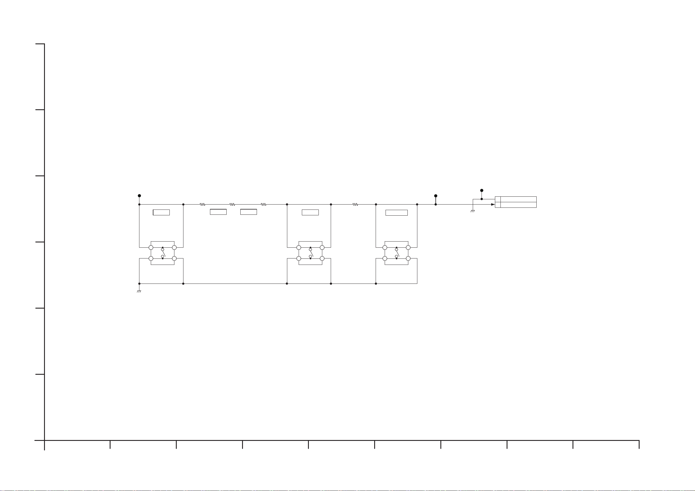
F
E
D
1
C
B
A
98765432
KEY2
GND
1
2
P6001
K1KA02AA0051
R6002
2.2K
R6003
3.3K
R6004
4.7K
S6004
K0F111A00472
R6001
1.5K
VOL+
TO P4002
MAIN P.C.B.
VOL-
UP
DOWN
LCD
TL6002
S_LCD_SW SCHEMATIC DIAGRAM
31
2 4
S6003
K0F111A00472
31
2 4
S6005
K0F111A00472
31
2 4
TL6001
TL6003
DMP-B200EB/EE/EG
11.5. LCD_SW SCHEMATIC DIAGRAM
42
Page 43
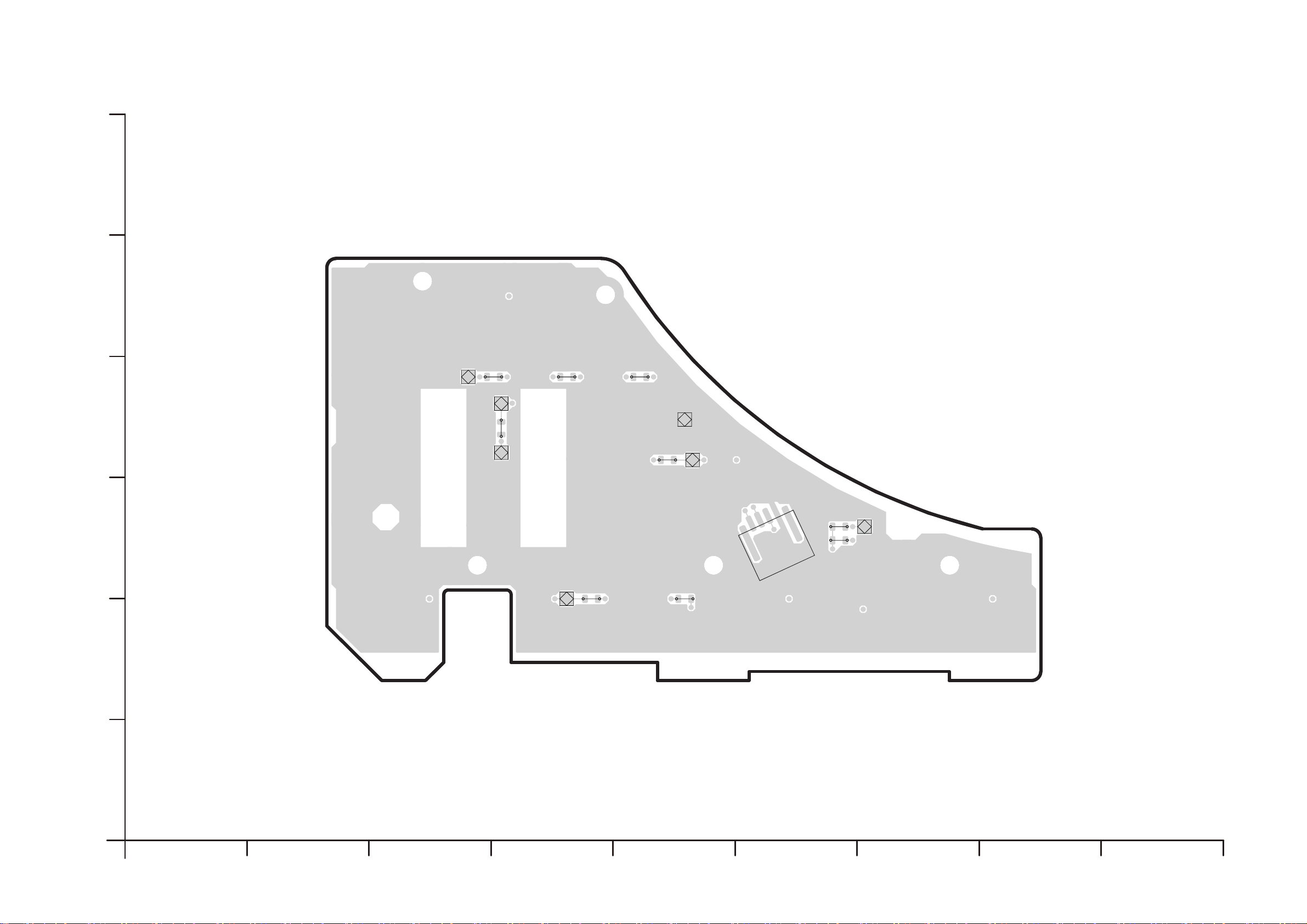
12 Printed Circuit Board
9876
F
543
2
1
E
D
C
B
A
(COMPONENT SIDE)
OPERATION P.C.B.
OPERATION P.C.B. (VEP76237A)
DMP-B200EB/EE/EG
TL6106
TL6103
TL6104
R6109
R6108
R6107
R6106
R6104
R6103
R6101
TL6101
R6102
P6101
1
2
3
4
TL6102
TL6107
TL6105
R6105
12.1. OPERATION P.C.B.
43
Page 44
F
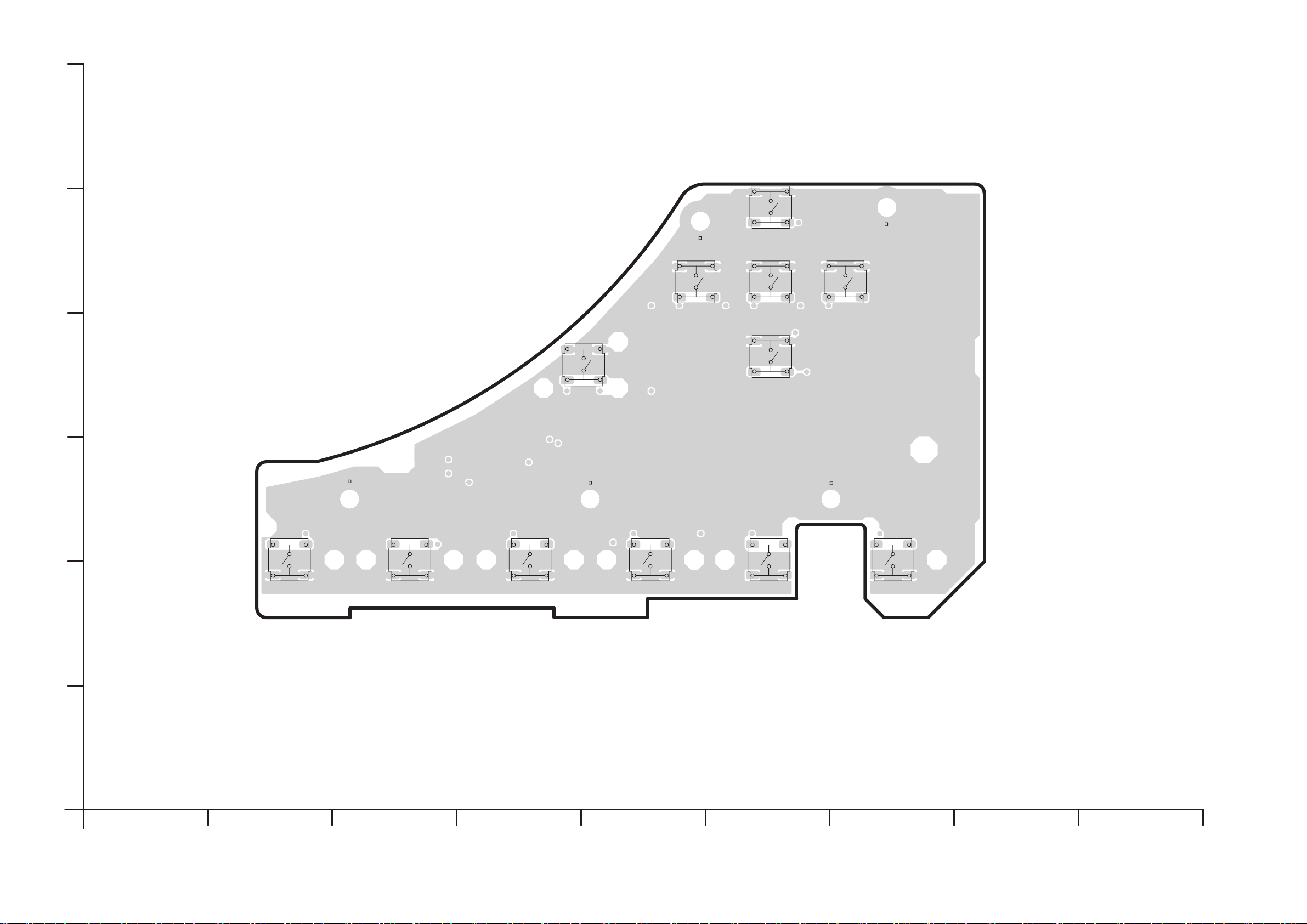
OPERATION P.C.B.
E
D
C
RL6105
4
3
S6108
RL6104
4
RL6102
S6110
4
3
2
1
3
4
2
3
1
4
3
S6106
S6111
S6107
2
1
S6112
4
2
3
1
2
1
RL6103
RL6101
2
1
1
2
S6101
3
4
1
2
S6103
3
4
1
2
S6102
3
4
1
2
S6104
3
4
1
2
S6105
3
4
1
2
S6109
3
4
B
A
(FOIL SIDE)
DMP-B200EB/EE/EG
OPERATION P.C.B. (VEP76237A)
1
2
543
9876
44
Page 45
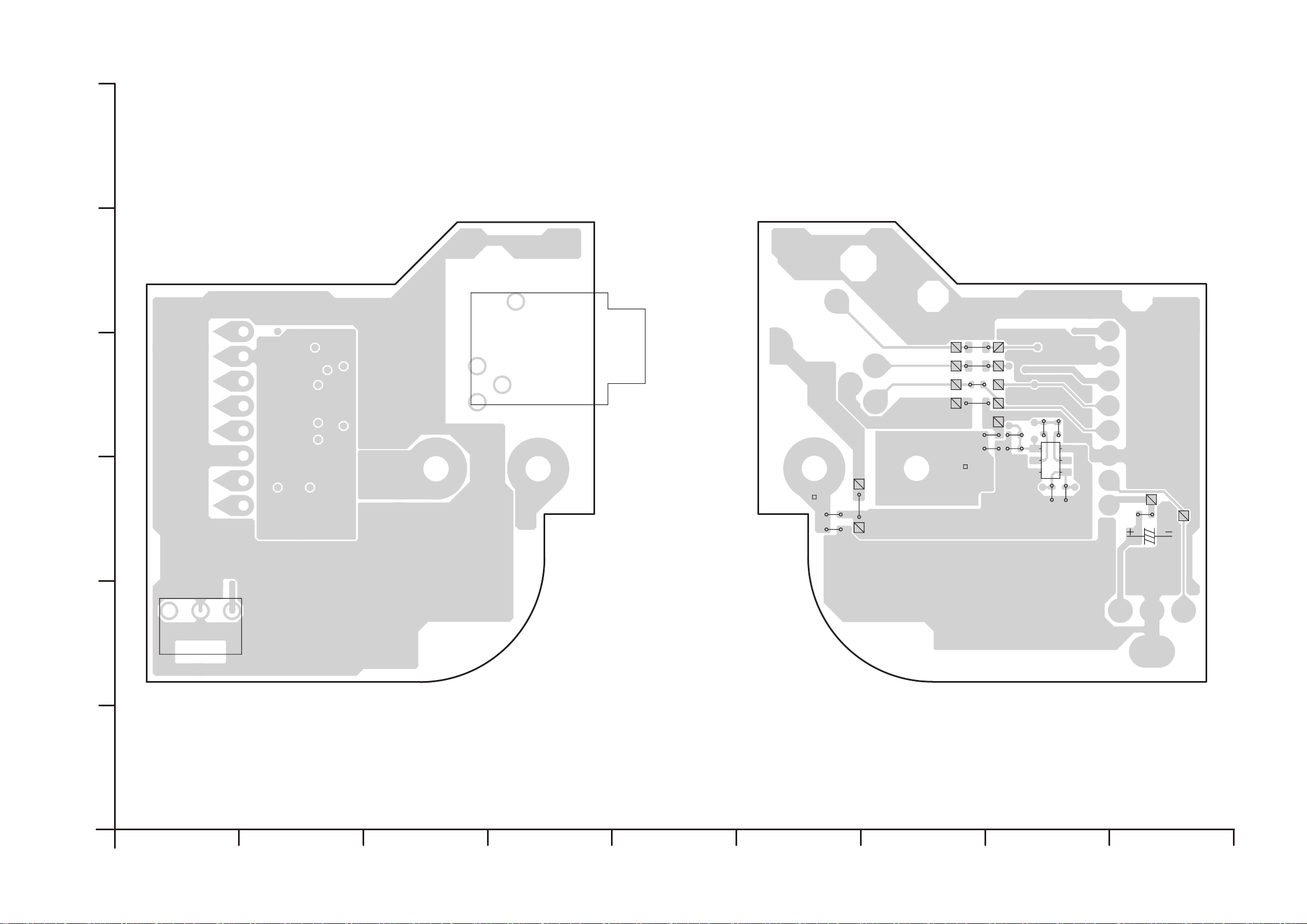
12.2. HP_REMOCON P.C.B.
E
D
C
F
HP REMOTE CONTROL P.C.B.
(COMPONENT SIDE)(FOIL SIDE)
2
RL4101
LB4194
LB4193
R4137
LB4192
CL4115
C4104
C4103
CL4110
CL4112
CL4113
CL4114
R4134
C4132
3
1
R4136
R4135
QR4123
4
6
R4133
C4131
CL4117
R4101
C4101
CL4116
JK4103
3
4
5
1
CL4127
RL4102
C4105
C4106
LB4190
CL4111
CL4128
CL4129
CL4131
CL4132
12 3
IR4101
B
A
DMP-B200EB/EE/EG
HP REMOTE CONTROL P.C.B. (VEP74125A)
1
2
543
45
9876
Page 46
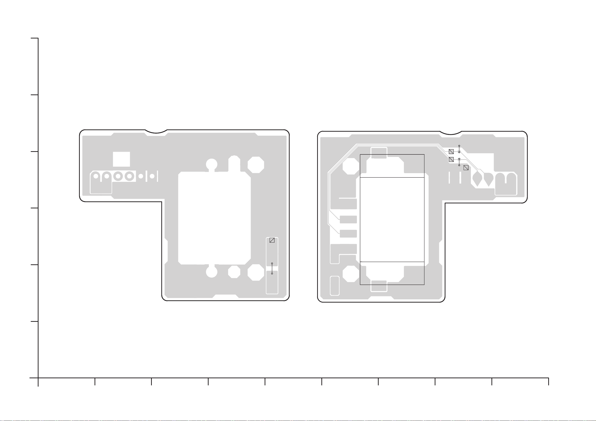
12.3. BAT-CONNECTOR P.C.B.
F
E
D
BAT-CONNECT P.C.B.
(FOIL SIDE) (COMPONENT SIDE)
4
CL1802
CL1803
C1802
C1801
CL1804
C
B
A
CL1801
IP1801
3
2
1
JK1801
DMP-B200EB/EE/EG
BAT-CONNECT P.C.B. (VEP71196A)
1
2
543
46
9876
Page 47
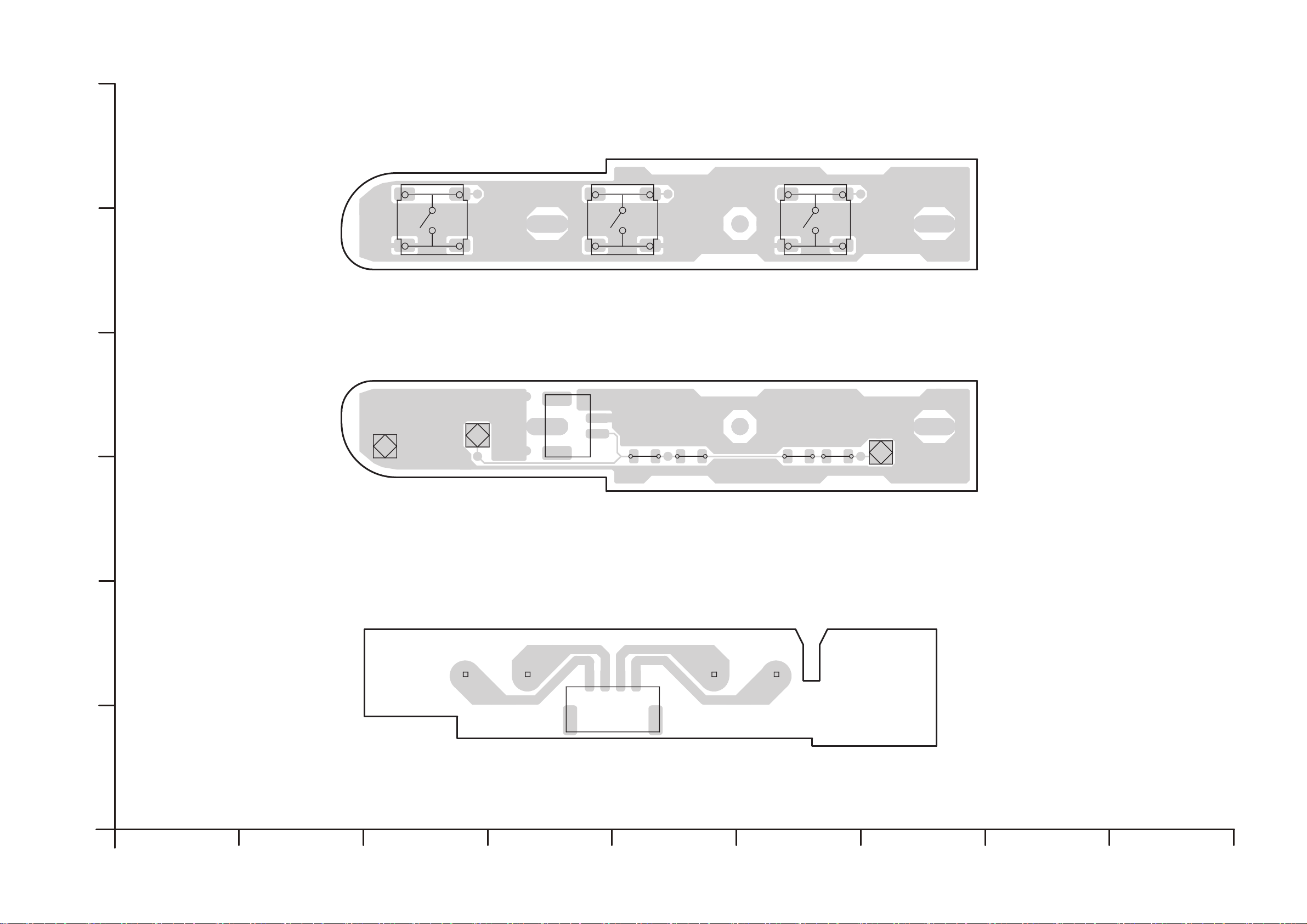
12.4. LCD_SW P.C.B. and SPEAKER P.C.B.
F
E
D
LCD SW P.C.B. (FOIL SIDE)
S6004
1
2
3
4
LCD SW P.C.B. (COMPONENT SIDE)
TL6003
TL6001
P6001
S6005
1
2
2
1
3
4
R6001 R6002 R6003 R6004
S6003
1
2
3
4
TL6002
C
B
A
SPEAKER P.C.B. (COMPONENT SIDE)
RL6001
1
2
RL6202
41
P6201
RL6203
543
RL6204
DMP-B200EB/EE/EG
LCD SW P.C.B. (VEP76238A)
SPEAKER P.C.B. (VEP74126A)
9876
47
Page 48
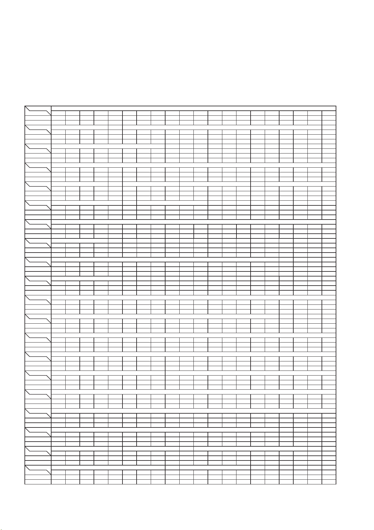
13 Appendix for Schematic Diagram
Ref No.
MODE
PLAY
STOP
Ref No.
MODE
PLAY
STOP
Ref No.
MODE
PLAY
STOP
Ref No.
MODE
PLAY
STOP
Ref No.
MODE
PLAY
STOP
Ref No.
MODE
PLAY
STOP
Ref No.
MODE
PLAY
STOP
Ref No.
MODE
PLAY
STOP
Ref No.
MODE
PLAY
STOP
Ref No.
MODE
PLAY
STOP
Ref No.
MODE
PLAY
STOP
Ref No.
MODE
PLAY
STOP
Ref No.
MODE
PLAY
STOP
Ref No.
MODE
PLAY
STOP
Ref No.
MODE
PLAY
STOP
Ref No.
MODE
PLAY
STOP
Ref No.
MODE
PLAY
STOP
Ref No.
MODE
PLAY
STOP
Ref No.
MODE
PLAY
STOP
Ref No.
MODE
PLAY
STOP
IC51301
IC51301
IC51301
123456789101112 1314151617181920
0000003.33.33.3003.3000003.200
0000003.33.33.3003.3000003.200
21 22 23 24 25 26 27 28 29 30 31 32 33 34 35 36 37 38 39 40
000000003.33.23.23.200003.3000
000000003.33.23.23.200003.3000
41 42 43 44 45 46 47 48
3.23.23.23.20000
3.23.23.23.20000
IC1001
IC1001
1234567891011121314151617181920
6.703.200000.803.27.64.53.30004.90011.7
6.703.200000.803.27.64.53.30004.90011.7
21 22 23 24
0004.9
0004.9
IC1002
1234567891011121314
2.5 1.8 0 3.2 6.7 11 11.8 11.8 11.8 0 1.6 1.0 2.0 2.5
2.5 1.8 0 3.2 6.7 11 11.8 11.8 11.8 0 1.6 1.0 2.0 2.5
IC1102
12345678
0.6 0.6 3.2 0 9.0 0 0.8 1.2
0.6 0.6 3.2 0 9.0 0 0.8 1.2
IC1201
IC1201
1234567891011121314151617181920
3.2 2.4 0.7 0.5 1.2 1.3 3.3 3.2 1.6 0.6 0.7 2.4 3.3 6.2 1.6 1.2 4.4 0
3.2 2.4 0.7 0.5 1.2 1.3 3.3 3.2 1.6 0.6 0.7 2.4 3.3 6.2 1.6 1.2 4.4 0
21 22 23 24
4.3 1.5 2.1 6.4
4.3 1.5 2.1 6.4
IC1401
1234
7.2 6.3 0 0
7.2 6.3 0 0
IC1451
5.0
5.0
11.9
11.9
1234
3.2 0 0 0
3.2 0 0 0
IC1454
12345
IC1452
12345
11.2 0 3.3 9.8 11.2
11.2 0 3.3 9.8 11.2
IC1461
12345
11.1 0 0 11.4 3.9
11.1 0 0 11.4 3.9
IC1601
IC1601
1234567891011121314151617181920
00003.6000000000000011.811.7
00003.6000000000000011.811.7
21 22 23 24
11.8 11.8 0 0
11.8 11.8 0 0
IC4001
12345678910111213141516
0.3 3.2 3.2 2.0 1.6 0.7 1.6 1.6 0 0 4.6 0 2.3 0 2.3 4.6
0.3 3.2 3.2 2.0 1.6 0.7 1.6 1.6 0 0 4.6 0 2.3 0 2.3 4.6
IC4002
12345
4.8 0 4.8 0 4.6
4.8 0 4.8 0 4.6
IC4008
IC4008
1234567891011121314151617181920
03.3000003.30001.601.6000003.3
03.3000003.30001.601.6000003.3
21 22 23 24 25 26 27 28 29 30 31 32 33 34 35 36
03.303.202.33.30.100000000
03.303.202.33.30.100000000
IC55005
IC55005
IC55005
1234567891011121314151617181920
0 11.5 11 0 0 2.5 0 0 3.3 0 0 0 0 0 0 4.8 0 0 0 0
IC55300
12345678
3.30000004.80000
21 22 23 24 25 26 27 28 29 30 31 32 33 34 35 36 37 38 39 40
004.800000000000000000
004.800000000000000000
41 42 43 44 45 46 47 48 49 50 51 52 53 54 55 56
00011.900000000011.9 11.9 0
00011.900000000011.9 11.9 0
IC55008
1234
0 4.8 2.6 3.2
0000
IC55009
1234
0 0 1.3 0
0 0 1.3 0
IC55901
IC56001
12345678
00000000
0000
0000
12345
3.3 1.3 1.3 5 9
3.3 1.3 1.3 5 9
5.0 0 1.3 0 9.3 9.300
5.0 0 1.3 0 9.3 9.300
0 0 0 4.3 3.4
0 0 0 4.3 3.4
13.1. Voltage and Waveform Chart
NOTE:
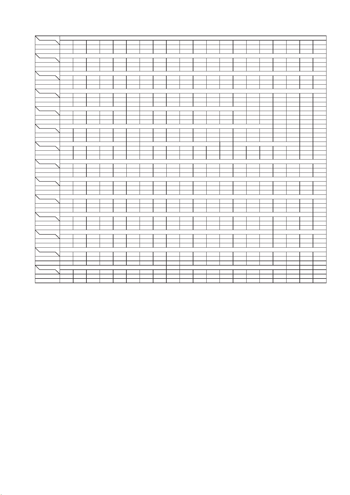
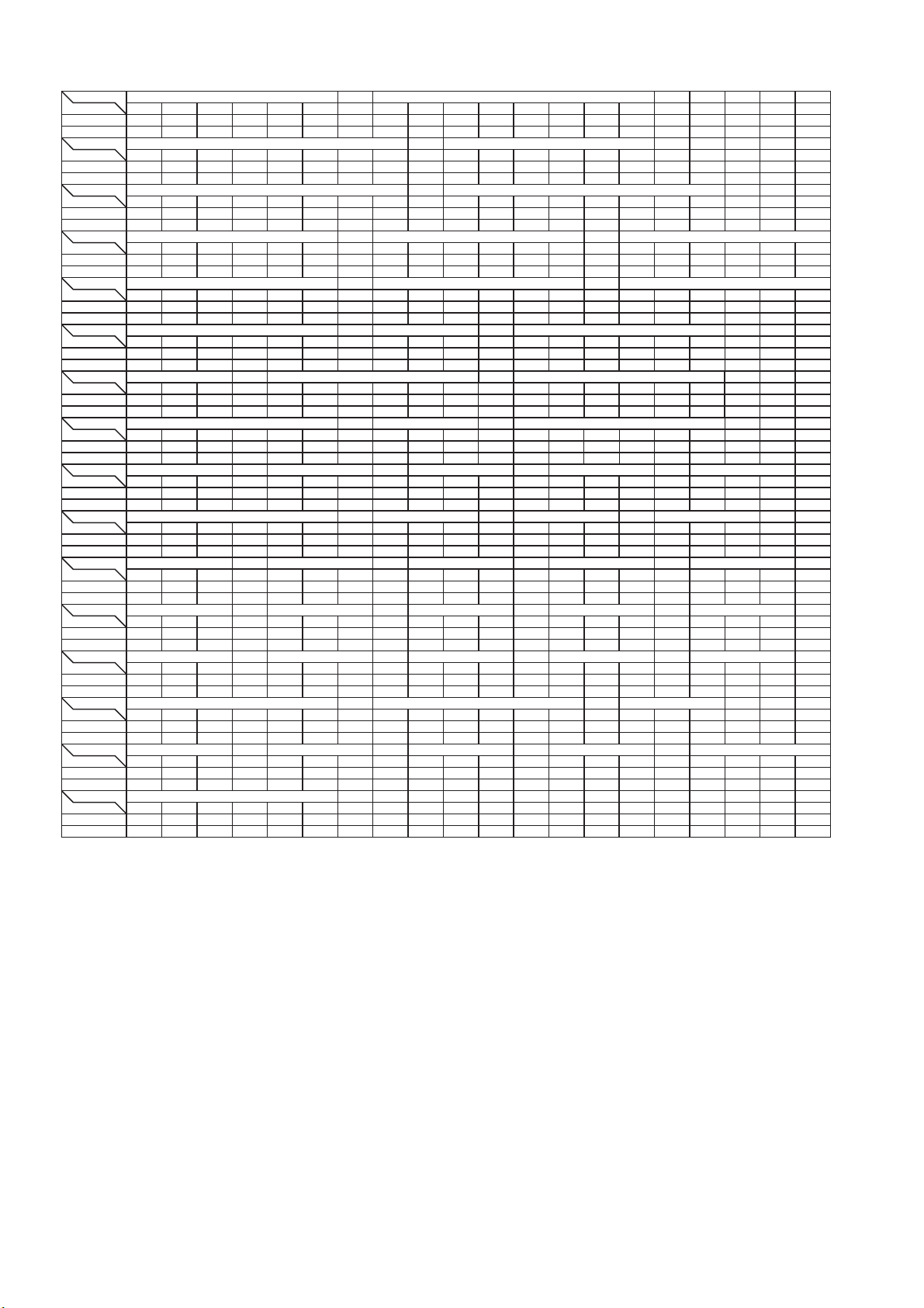
Circuit voltage and waveform described herein shall be regarded as reference information when probing defect point, because it
may differ from an actual measuring value due to difference of Measuring instrument and its measuring condition and product
itself.
13.1.1. Main P.C.B.
48
Page 49
Ref No.
MODE
PLAY
STOP
Ref No.
MODE
PLAY
STOP
Ref No.
MODE
PLAY
STOP
Ref No.
MODE
PLAY
STOP
Ref No.
MODE
PLAY
STOP
Ref No.
MODE
PLAY
STOP
Ref No.
MODE
PLAY
STOP
Ref No.
MODE
PLAY
STOP
Ref No.
MODE
PLAY
STOP
Ref No.
MODE
PLAY
STOP
Ref No.
MODE
PLAY
STOP
Ref No.
MODE
PLAY
STOP
Ref No.
MODE
PLAY
STOP
Ref No.
MODE
PLAY
STOP
1234567891011121314151617181920
0 3.3 0 3.3 0 01.6 3.3 3.3 0 3.3 1.3 1.6 0 0 0 3.3 0 1.8 3.3
0 3.3 0 3.3 0 01.6 3.3 3.3 0 3.3 1.3 1.6 0 0 0 3.3 0 1.8 3.3
21 22 23 24 25 26 27 28 29 30 31 32 33 34 35 36 37 38 39 40
3.3 0 0 0 0 3.3 3.3 3.3 3.3 0 3.3 3.3 3.2 3.3 3.2 3.2 0 0 0 3.2
3.3 0 0 0 0 3.3 3.3 3.3 3.3 0 3.3 3.3 3.2 3.3 3.2 3.2 0 0 0 3.2
41 42 43 44 45 46 47 48 49 50 51 52 53 54 55 56 57 58 59 60
0 3.3 3.3 0 3.2 0.2 3.2 2.4 3.3 3.3 3.2 3.3 3.3 0 0 3.3 3.3 3.3 3.3 3.3
0 3.3 3.3 0 3.2 0.2 3.2 2.4 3.3 3.3 3.2 3.3 3.3 0 0 3.3 3.3 3.3 3.3 3.3
61 62 63 64 65 66 67 68 69 70 71 72 73 74 75 76 77 78 79 80
3.003.200000003.33.23.203.200003.2
3.003.200000003.33.23.203.200003.2
12345
0 0 0 3.3 3.3
0 0 0 3.3 3.3
12345678910111213141516
3.2 0.4 0.8 0 0 3.33.3 0 3.3 1.1 0.3 1.1 3.3 3.2 0 1.1
3.2 0.4 0.8 0 0 3.33.3 0 3.3 1.1 0.3 1.1 3.3 3.2 0 1.1
12345
0 0 0 3.3 3.3
0 0 0 3.3 3.3
1234567891011121314151617181920
0 0.4 0.9 0.8 1.6 2.5 0.4 0 0.4 0 0.7 0.4 0.3 0.3 0.3 0.3 0.3 0.2 0.2 2.5
0 0.4 0.9 0.8 1.6 2.5 0.4 0 0.4 0 0.7 0.4 0.3 0.3 0.3 0.3 0.3 0.2 0.2 2.5
21 22 23 24 25 26 27 28 29 30 31 32 33 34 35 36 37 38 39 40
0 0.2 0.3 0.3 0.2 0.4 0.8 0.3 0.8 0.2 2.4 2.4 0.8 0 4.7 0 4.7 0.2 1.2 4.7
0 0.2 0.3 0.3 0.2 0.4 0.8 0.3 0.8 0.2 2.4 2.4 0.8 0 4.7 0 4.7 0.2 1.2 4.7
41 42 43 44 45 46 47 48 49 50 51 52 53 54 55 56 57 58 59 60
1.24.84.83.33.200002.400.60.313.23.23.2000
1.24.84.83.33.200002.400.60.313.23.23.2000
61 62 63 64 65 66 67 68 69 70 71 72 73 74 75 76 77 78 79 80
0.2 0.2 0 0 2.8 3.2 3.2 4.7 0 0 3.2 0.6 2.6 2.6 2.6 2.6 1.2 2.6 0 0
0.2 0.2 0 0 2.8 3.2 3.2 4.7 0 0 3.2 0.6 2.6 2.6 2.6 2.6 1.2 2.6 0 0
81 82 83 84 85 86 87 88 89 90 91 92 93 94 95 96 97 98 99 100
3.2 2.7 0.5 1.2 1.2 1.2 1.2 1.2 0.3 0 1.2 1.2 1.2 1.2 1.2 0.5 1.5 1.0 0.1 3.2
3.2 2.7 0.5 1.2 1.2 1.2 1.2 1.2 0.3 0 1.2 1.2 1.2 1.2 1.2 0.5 1.5 1.0 0.1 3.2
101 102 103 104 105 106 107 108 109 110 111 112 113 114 115 116 117 118 119 120
0 3.2 0 0 1.3 1.2 1.6 1.3 2.0 0.6 0 0 2.5 0 0 0 1.3 1.3 4.7 4.7
0 3.2 0 0 1.3 1.2 1.6 1.3 2.0 0.6 0 0 2.5 0 0 0 1.3 1.3 4.7 4.7
121 122 123 124 125 126 127 128
0 2.3 2.3 4.6 1.4 0 2.5 0
0 2.3 2.3 4.6 1.4 0 2.5 0
IC57002
IC57007
IC8803
12345678
0 0 0 0 3.2 3.2 0 3.2
0 0 0 0 3.2 3.2 0 3.2
IC57006
123456
00003.33.3
00003.33.3
IC57001
IC57001
IC57001
IC57001
IC57005
IC57031 IC57032
IC8803
IC8803
IC8803
IC8803
IC8803
IC8803
12345678
0.2 0.9 3.3 0 0.4 0.8 3.2 3.2
0.2 0.9 3.3 0 0.4 0.8 3.2 3.2
12345
0 0 0 3.2 3.2
0 0 0 3.2 3.2
IC8804
49
Page 50
Ref No.
MODE
PLAY
STOP
Ref No.
MODE
PLAY
STOP
Ref No.
MODE
PLAY
STOP
Ref No.
MODE
PLAY
STOP
Ref No.
MODE
PLAY
STOP
Ref No.
MODE
PLAY
STOP
Ref No.
MODE
PLAY
STOP
Ref No.
MODE
PLAY
STOP
Ref No.
MODE
PLAY
STOP
Ref No.
MODE
PLAY
STOP
Ref No.
MODE
PLAY
STOP
Ref No.
MODE
PLAY
STOP
Ref No.
MODE
PLAY
STOP
Ref No.
MODE
PLAY
STOP
Ref No.
MODE
PLAY
STOP
Ref No.
MODE
PLAY
STOP
123456
9.2 9.2 11.4 11.9 9.2 9.2
9.2 9.2 11.4 11.9 9.2 9.2
12345678
3.3 4.5 0 3.4 3.3 3.3 11.8 11.8
3.3 4.5 0 3.4 3.3 3.3 11.8 11.8
12345678
1.9 2.6 0 4.0 1.9 1.9 11.8 11.8
1.9 2.6 0 4.0 1.9 1.9 11.8 11.8
123456
-1.0 -1.0 11.8 0 0 0
-1.0 -1.0 11.8 0 0 0
123456
0 -0.9 -0.8 -0.8 -0.8 0
0 -0.9 -0.8 -0.8 -0.8 0
123456
11.9 11.9 3.8 11.9 11.9 11.9
11.9 11.9 3.8 11.9 11.9 11.9
Q1454
123
0 0 11.9
0 0 11.9
123456
0000000
0000 0
Q55902
123
000
000
123456
2.5 2.5 2.7 4.8 2.5 2.5
2.5 2.5 2.7 4.8 2.5 2.5
QR1403
123
0 0 5.8
0 0 5.8
QR1601
123
000
000
QR4004
123
000
000
123456
0 0.7 0 0 0.7 0
0 0.7 0 0 0.7 0
QR55901
123
4.8 0 0
4.8 0 0
123456
4.7 4.7 1.5 4.7 4.7 4.7
4.7 4.7 1.5 4.7 4.7 4.7
Q1001
Q1004
Q1201
Q1401
Q1404
Q1451
123456
0 0 11.6 11.9 0 0
Q1603 Q1604
Q8802
QR4033
QR8808
0 0 11.6 11.9 0 0
Q56001
123
3.2 0 0
3.2 0 0 4.0 3.5 3.5 4.5 0 0 0 0 0
QR1404
123
3.2
00
00
3.2
QR1602
123
000
000
QR4005 QR4013
123
0 0 4.6
0 0 4.6
QR8801
123
0 0 3.2
0 0 3.2
12345678
4.9 6.7 0 2.8 5.0 5.0 11.8 0
4.9 6.7 0 2.8 5.0 5.0 11.8 0
123456
0.9 0.9 11.7 9.0 0.8 0.8
0.9 0.9 11.7 9.0 0.8 0.8
123456
11.9 11.9 0.1 11.8 11.8 11.9
11.9 11.9 0.1 11.8 11.8 11.9
123
3.4 7.7 11
3.4 7.7 11
Q1601
123
000
000
123
3.2
3.2
123456
0 0.1 -0.4 0 0.5 0
0 0.1 -0.4 0 0.5 0
Q1002
123456
9.0 9.0 0 0 9.0 9.0
9.0 9.0 0 0 9.0 9.0
12345678
1.3 1.9 0 4.3 1.3 1.3 11.8 11.8
1.3 1.9 0 4.3 1.3 1.3 11.8 11.8
Q1402
Q1405
Q1452
Q56002
123
4.0 3.5 3.5
QR1001
00
00
QR1452
123
0 11.2 0
0 11.2 0
QR1603
123
000
000
123
0 3.3 0
0 3.3 0
QR4123
QR8802
123
0 0 3.2
0 0 3.2
Q1101
Q1202
123456
3.3 3.3 0.3 3.3 3.3 3.3
3.3 3.3 0.3 3.3 3.3 3.3
123456
000000
0000 0
123456
0 0 4.0 4.0 0 0
0 0 4.0 4.0 0 0
QR1401
123
0 3.1 0
0 3.1 0
Q1453
Q1602
Q55901
Q56003
123
4.5 0 0
QR1453 QR1454
123
0.2 3.2 0
0.2 3.2 0
QR1604
123
000
000
QR4014
123
0 0 4.6
0 0 4.6
QR8803
123
0 0 3.2
0 0 3.2
123456
11.8 11.8 3.8 11.8 11.8 11.8
11.8 11.8 3.8 11.8 11.8 11.8
123456
11.8 11.8 0 11.7 11.7 11.7
11.8 11.8 0 11.7 11.7 11.7
QR55006
123
0 4.8 4.8
0 4.8 4.8
Q1403
Q1406
0
Q56004
123
000
QR1402
123
0 3.1 0
0 3.1 0
123
3.8 11.9 11.9
3.8 11.9 11.9
QR4003
123
3.2 3.3 0
3.2 3.3 0
50
Page 51
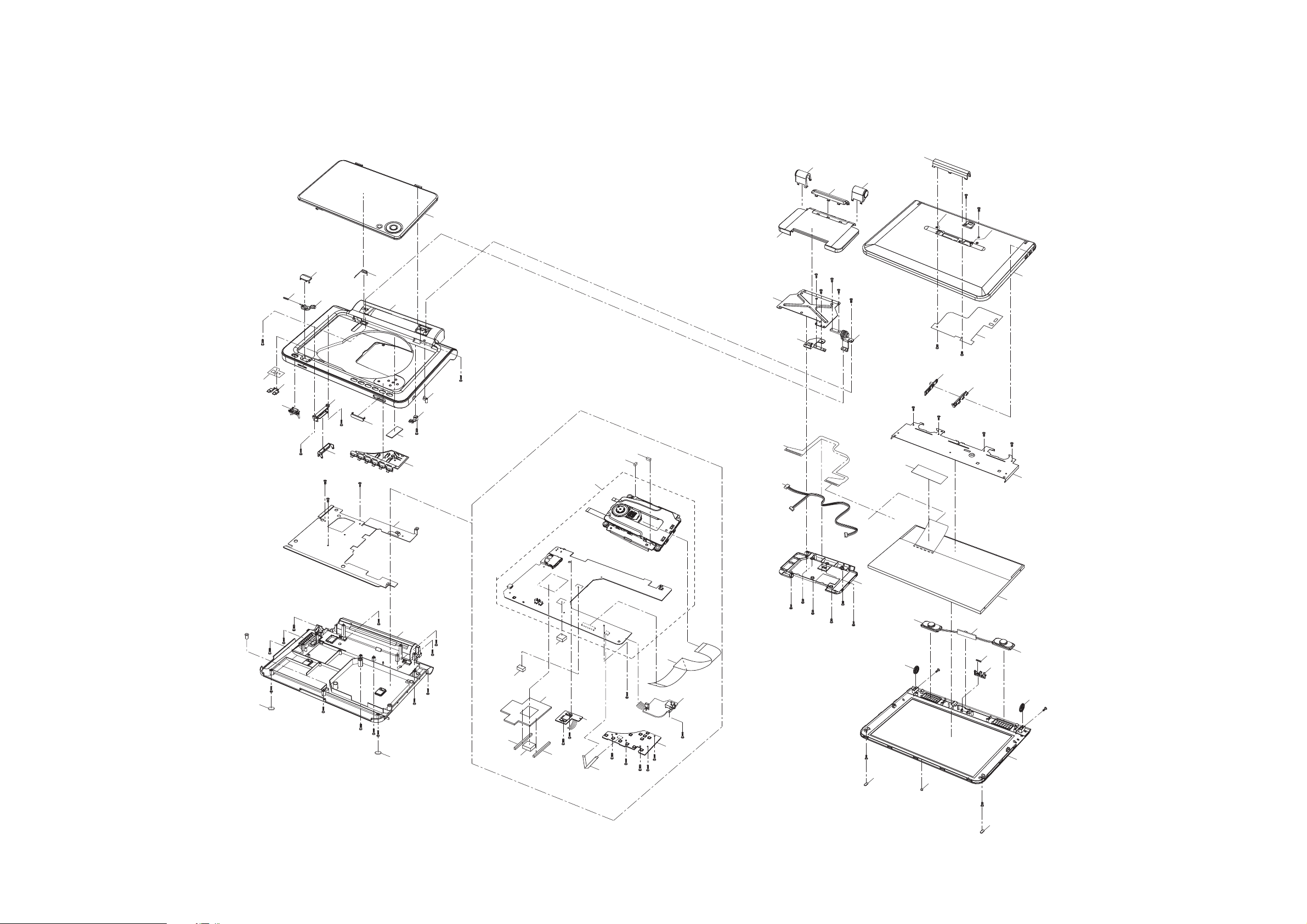
14 Exploded View and Replacement Parts List
48
37
33
31
36
35
94
94
94
94
10
11
30
34
38
32
22
91
93
93
29
93
93
92
92
92
92
92
92
92
92
93
93
24
16
20
19
28
28
25
27
21
23
26
26
18
6
15
7
59
56
54
40
9
5
3
8
44
43
45
66-1
66-2
66-2
50
57
49
42
47
55
51
52
93
93
93
93
93
65
93
93
93
93
93
93
93
93
93
93
93
92
92
92
92
92
92
92
93
93
92
92
92
92
92
92
92
92
92
46
63
62
61
61
53
58
60
4
41
66
(B200EB/EG)
(B200EB/EG)
(B200EB/EG)
14.1. Exploded Views and Mechanical Replacement Parts List
14.1.1. Casing Parts & Mechanism Section
51
Page 52
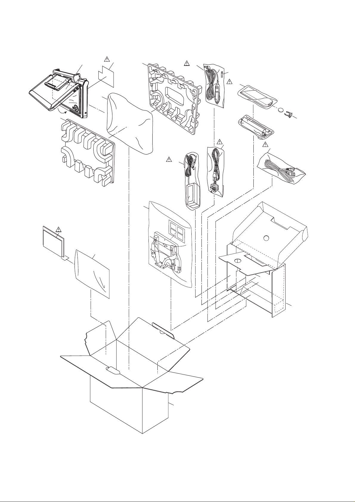
14.1.2. Packing & Accessories Section
PC1
A1
A1-1
A4
A10
PC8
PC4
PC2
PC7
A5
A2
PC3
A7
A2
(B200EE/EG)
(B200EB)
PC9
A8
A8-1
A16
52
Page 53
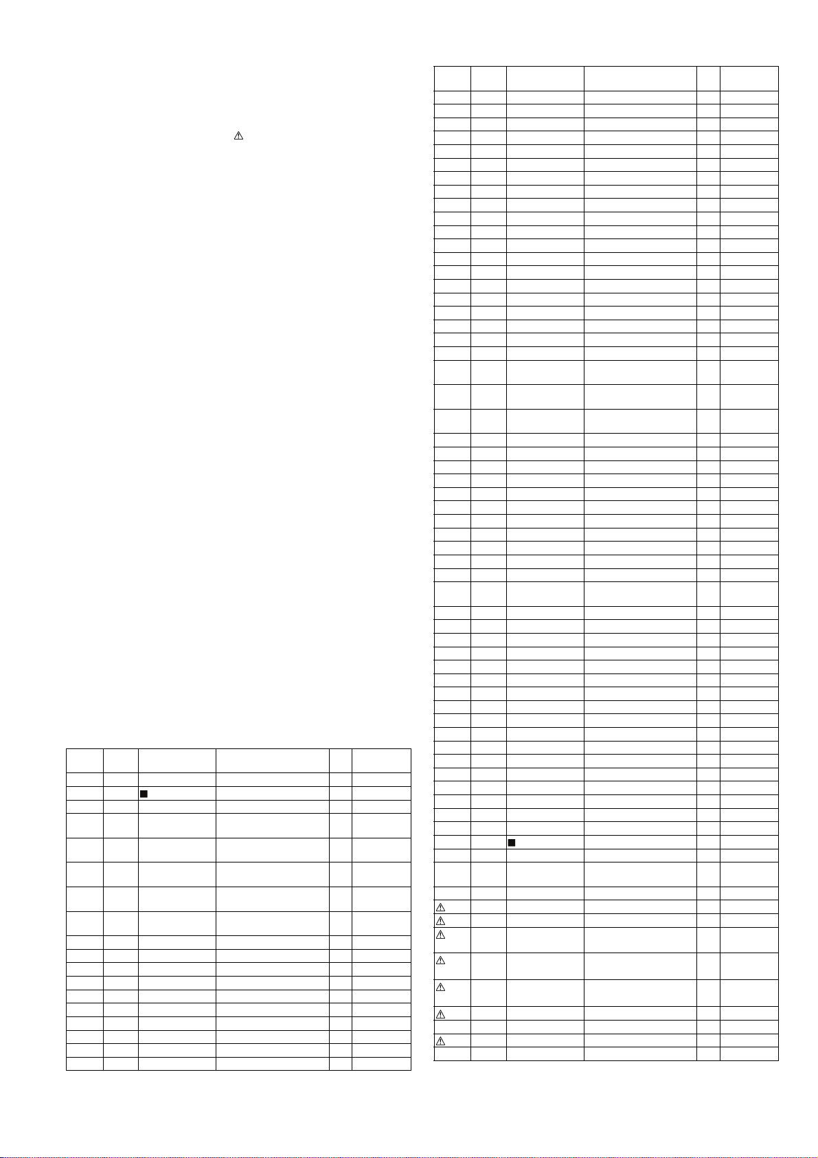
14.1.3. Mechanical Replacement Parts List
Notes:
*Important safety notice:
Components identified by mark have special character-
istics important for safety.
Furthermore, special parts which have purposes of
fire-retardant (resistors), high-quality sound (capacitors),
low-noise (resistors), etc. are used.
When replacing any of components, be sure to use only
manufacture’s specified parts shown in the parts list.
*Warning: This product uses a laser diode. Refer to caution
statements.
*Capacity values are in microfarads (μF) unless specified
otherwise, P=Pico-farads (pF), F=Farads (F).
*Resistance values are in ohms, unless specified otherwise,
1K=1,000 (OHM), 1M=1,000k (OHM).
*The marking (RTL) indicates the retention time is limited
for this item. After the discontinuation of this assembly in
production, it will no longer be available.
*"(IA)-(IC)" marks in Remarks indicate languages of instruc-
tion manuals. [ (IA): English; (IB): Russian; (IC): Genman,
French, Spanish, Italian, Swedish, Dutch, Danish]
*All parts are supplied by CHPAVC.
E.S.D.. standards for Electrostatically Sensitive
Devices, refer to “PREVENTION OF ELECTROSTATIC
DISCHARGE (ESD) TO ELECTROSTATICALLY
SENSITIVE (ES) DEVICES” section.
Notes:
*Parts indicated with "JIG & ADJ" in the Remarks column
are necessary to adjustment value initialization adjust. This
adjustment software can be downloaded from "Support
Information from NWBG/VDBG-PAVC" web-site in "TSN
system", together with instructions of "BD Drive Adjustment"
including preparations and connections etc.
Safety
Ref.
No.
3 VEP76237A OPERATION P.C.B. 1 (RTL)
4 VEP71196A BAT-CONNECT P.C.B. 1 (RTL)
5 VEP74125A HP REMOTE CONTROL
6 VEP74126A SPEAKER P.C.B. 1 (RTL)
7 VEP76238A LCD SW P.C.B. 1 (RTL)
8 REZ1976-1 FFC 1
9 REZ1981 FFC 1
10 REZ2033 MONIITOR CABLE 1
11 REZ2034 MONITOR KEY CABLE 1
15 RMF0441 SPACER 1
16 RMA2234 MONITOR ANGLE 1
18 L0AA01B00012 SPEAKER B (R) 1
19 L0AA01B00015 SPEAKER A (L) 1
20 L5EDD2Q00012 LCD PANEL 1
21 RFKGB200K MONITOR CABINET 1
Part No. Part Name &
Description
CASING
P.C.B.
Pcs Remarks
1 (RTL)
E.S.D.
E.S.D.
E.S.D.
E.S.D.
E.S.D.
Safety
Ref.
No.
22 RGQ0553-K MONITOR COVER ASS'Y 1
23 RGQ0587-K PROTECT CUSHION 1
24 RGU2661-K1 MONITOR BUTTON 1
25 RMB0835 LOCK LEVER SPRING 1
26 RMG0808-K PROTECT CUSHION(B) 2
27 RML0721-1 MONO ARM LOCK LEVER 1
28 RMR1959-K ROLLER 2
29 RMZ1089 MONITOR SHEET 1
30 RGQ0556-K1 MONO ARM 1
31 RGQ0557-K MONO ARM COVER 1
32 RGQ0558-K HINGE COVER 1
33 RGQ0559-K MONITOR CUSSION 1
34 RKC0027-2 FRICTION HINGE (A) 1
35 RKC0028 FRICTION HINGE (B) 1
36 RMA2233 HINGE PLATE 1
37 RGQ0554-K SHAFT HOLDER (L) 1
38 RGQ0555-K SHAFT HOLDER (R) 1
40 RMQ1735 CONDUCTION CUSHION 1
41 RMQ1831 CONDUCTION CUSHION 1
42 RMV0365 LED SHEET 1
43 RSC0924 HEAT RADIATION
44 RSC0999 HEAT RADIATION
45 RSC1000 HEAT RADIATION
46 RMQ1862 COPPER SHEET 1
47 RGL0731-1W LIGHTING PIECE 1
48 RFKKB200EB DISC COVER ASS'Y 1
49 RGQ0560-K SD HOLDER 1
50 RGQ0563-K STOPPER PIECE 1
51 RKF0870-K1 SD COVER 1
52 RGU2662-K1 OPERATION BUTTON 1
53 RGU2663-K1 OPEN BUTTON 1
54 RGU2664-K LCD OFF BUTTON 1
55 RGU2669-1S POWER BUTTON 1
56 RKM0622A-K MAIN CABINET 1
57 RKW0914-R REMOTE SENSOR WIN-
58 RMB0834 OPEN BUTTON SPRING 1
59 RMB0912 OPEN SPRING 1
60 RMR1960-K RELEASE LOCK LEVER 1
61 RKA0245-K FOOT RUBBER 2
62 RKS0465-K BOTTOM CABINET 1
63 RMY0400 HEAT SINK PLATE 1
65 THNX042 NUT1 1
66 RFKNB200EB TRV U + Main P.C.B. 1 B200EB
66 RFKNB200EG TRV U + Main P.C.B. 1 B200EG
66-1 RSC0985 SHIELD PLATE B 1 B200EB/EG
66-2 RMQ1715 CONDUCTION CUSHION 2 B200EB/EG
66 RFKNB200EE TRV U + Main P.C.B. 1 B200EE
91 XQN17+B4FN SCREW 1
92 XQN17+BG4FNJ SCREW 24
93 XTN17+6GFJK SCREW 24
94 XYN2+C35FN SCREW 4
A1 N2QAJC000019 REMOTE CONTROL
A1-1 ETR006632001 BATTERY HOLDER 1
A2 K2CT2CA00007 AC CORD 1 B200EB
A2 K2CQ2CA00006 AC CORD 1 B200EE/EG
A4 VQT3C18 OPERATING INSTRUC-
A4 VQT3C19 OPERATING INSTRUC-
A4 VQT3C17 OPERATING INSTRUC-
A5 RFEA219W-AA AC ADAPTOR 1
A7 RXQ1820 BRACKET UNIT 1
A8 RFEC207P-AB CAR DC CABLE 1
A8-1 EF-A50201511 FUSE 1
Part No. Part Name &
Description
PLATE A
PLATE C
PLATE B
DOW
ACCESSORY
ASS'Y
TIONS
TIONS
TIONS
Pcs Remarks
1
1
1
1
1
1 B200EB/EG
(IA)
1
B200EE
(IB)
1
B200EG
(IC)
53
Page 54

Safety
Ref.
No.
A10 RPFC0031-B POLYETHYLENE
A16 RGN3009B-K NAME LABEL 1 B200EB/EG
A16 RGN3009D-K1 NAME LABEL 1 B200EE
PC1 RPK2908 PACKING CASE 1 B200EB
PC1 RPK2910-1 PACKING CASE 1 B200EE
PC1 RPK2909 PACKING CASE 1 B200EG
PC2 RPFC0128 POLYETHYLENE FILM 1
PC3 RPQF0346 ACCESSORY BOX 1
PC4 RPFC0115B POLYETHYLENE BAG 1
PC7 RPN2152A CUSHION (A) 1
PC8 RPN2152B CUSHION (B) 1
PC9 RPQ2652 SHEET 1
Part No. Part Name &
Description
BAG(UNIT)
PACKING
Pcs Remarks
1
54
Page 55
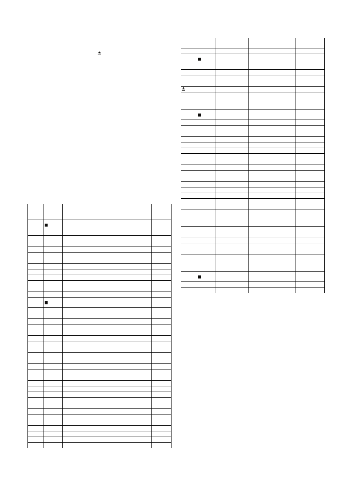
14.2. Electrical Replacement Parts List
Notes:
*Important safety notice:
Components identified by mark have special characteristics important for safety.
Furthermore, special parts which have purposes of
fire-retardant (resistors), high-quality sound (capacitors),
low-noise (resistors), etc. are used.
When replacing any of components, be sure to use only
manufacture’s specified parts shown in the parts list.
*Warning: This product uses a laser diode. Refer to caution
statements.
*Capacity values are in microfarads (μF) unless specified
otherwise, P=Pico-farads (pF), F=Farads (F).
*Resistance values are in ohms, unless specified otherwise,
1K=1,000 (OHM), 1M=1,000k (OHM).
*The marking (RTL) indicates the retention time is limited
for this item. After the discontinuation of this assembly in
production, it will no longer be available.
*All parts are supplied by CHPAVC.
E.S.D. standards for Electrostatically Sensitive Devices,
refer to “PREVENTION OF ELECTROSTATIC DISCHARGE (ESD) TO ELECTROSTATICALLY
SENSITIVE (ES) DEVICES” section.
Safety Ref.
No.
Part No. Part Name &
Description
Pcs Remarks
Safety Ref.
No.
C1801 F1G1E1020001 25V 1000P 1
C1802 F1G1E1020001 25V 1000P 1
IP1801 D1JBR012A007 IC PROTECTOR 1
JK1801 G1C220KA0138 JACK 1
C4101 F3F0J476A032 6.3V 47U 1
C4103 F1G1H1010001 50V 100P 1
C4104 F1G1H1010001 50V 100P 1
C4105 F1G1H1010001 50V 100P 1
C4106 F1G1H1010001 50V 100P 1
C4131 F1G1C1030008 16V 0.01U 1
C4132 F1G1C1030008 16V 0.01U 1
IR4101 PNA4811M00YD REMOTE SENSOR 1
JK4103 K2HC103B0213 JACK 1
LB4190 J0JBC0000028 COIL 1
LB4192 J0JBC0000028 COIL 1
LB4193 J0JBC0000028 COIL 1
LB4194 J0JBC0000028 COIL 1
Part No. Part Name &
VEP71196A BAT-CONNECT P.C.B.
VEP74125A
Description
HP REMOTE CONTROL
P.C.B.
Pcs Remarks
(RTL)
E.S.D.
(RTL)
E.S.D.
VEP76238A LCD SW P.C.B.
R6001 ERJ3GEYJ152V 1/10W 1.5K 1
R6002 ERJ3GEYJ222V 1/10W 2.2K 1
R6003 ERJ3GEYJ332V 1/10W 3.3K 1
R6004 ERJ3GEYJ472V 1/10W 4.7K 1
P6001 K1KA02AA0051 CONNECTOR(2P) 1
S6003 K0F111A00472 SWITCH 1
S6004 K0F111A00472 SWITCH 1
S6005 K0F111A00472 SWITCH 1
VEP76237A OPERATION P.C.B.
P6101 K1MY04BA0041 CONNECTOR(4P) 1
R6101 ERJ3GEYJ152V 1/10W 1.5K 1
R6102 ERJ3GEYJ222V 1/10W 2.2K 1
R6103 ERJ3GEYJ332V 1/10W 3.3K 1
R6104 ERJ3GEYJ472V 1/10W 4.7K 1
R6105 ERJ3GEYJ332V 1/10W 3.3K 1
R6106 ERJ3GEYJ152V 1/10W 1.5K 1
R6107 ERJ3GEYJ222V 1/10W 2.2K 1
R6108 ERJ3GEYJ332V 1/10W 3.3K 1
R6109 ERJ3GEYJ472V 1/10W 4.7K 1
S6101 K0F111A00472 SWITCH 1
S6102 K0F111A00472 SWITCH 1
S6103 K0F111A00472 SWITCH 1
S6104 K0F111A00472 SWITCH 1
S6105 K0F111A00472 SWITCH 1
S6106 K0F111A00472 SWITCH 1
S6107 K0F111A00472 SWITCH 1
S6108 K0F111A00472 SWITCH 1
S6109 K0F111A00472 SWITCH 1
S6110 K0F111A00472 SWITCH 1
S6111 K0F111A00472 SWITCH 1
S6112 K0F111A00472 SWITCH 1
(RTL)
E.S.D.
(RTL)
E.S.D.
QR4123 B1GFGCAA0001 TRANSISTOR 1 E.S.D.
R4101 ERJ2GEJ470X 1/16W 47 1
R4133 ERJ2GEJ472X 1/16W 4.7K 1
R4134 ERJ2GEJ472X 1/16W 4.7K 1
R4135 ERJ2GEJ561X 1/16W 560 1
R4136 ERJ2GEJ561X 1/16W 560 1
R4137 ERJ2GEJ102X 1/16W 1K 1
VEP74126A SPEAKER P.C.B.
P6201 K1KA04AA0051 CONNECTOR(4P) 1
(RTL)
E.S.D.
55
Page 56

15 Schematic Diagram for printing with A4 size
56
 Loading...