

Page 1
ORDER NO. CPD0611207C2
Notebook Computer
Model No. CF-30 SERIES
This is the Service Manual for
the following areas.
E …for U.K.
G …for Germany
F …for France
T … for Italy
P … for Spain
S … for Sweden
L … for Belgium
2 … for UK
Model No. CF-30CTQAZ 1 2
1: Operation System
B: Microsoft® Windows® XP Professional
L: Microsoft® Windows® XP Professional MUI
2: Area
E /G /F /T /P /S /L /2: Refer to above area table
© 2006 Matsushita Electric Industrial Co., Ltd. All rights reserved.
Unauthorized copying and distribution is a violation of law.
Page 2

WARNING
1
For U.K.
This apparatus must be earthed for your safety.
To ensure safe operation the three-pin plug must be inserted only into a standard three-pin power point
which is effectively earthed through the normal household wiring.
Extension cords used with the equipment must be three-core and be correctly wired to provide connection to earth. Wrongly wired extension cords are a major cause of fatalities.
The fact that the equipment operates satisfactorily does not imply that the power point is earthed and
that the installation is completely safe.
For your safety, if you have any doubt about the effective earthing of the power point, consult a qualified electrician.
FOR YOUR SAFETY PLEASE READ THE FOLLOWING TEXT CAREFULLY
This appliance is supplied with a moulded three pin mains plug for your safety and convenience.
A 3 amp fuse is fitted in this plug.
Should the fuse need to be replaced please ensure that the replacement fuse has a rating of 3 amps and
that it is approved by ASTA or BSI to BS 1362.
Check for the ASTA mark
If the plug contains a removable fuse cover you must ensure that it is refitted when the fuse is replaced.
If you lose the fuse cover the plug must not be used until a replacement cover is obtained.
A replacement fuse cover can be purchased from your local Panasonic Dealer.
IF THE FITTED MOULDED PLUG IS UNSUITABLE FOR THE SOCKET OUTLET IN YOUR
HOME THEN THE FUSE SHOULD BE REMOVED AND THE PLUG CUT OFF AND DISPOSED
OF SAFELY.
THERE IS A DANGER OF SEVERE ELECTRICAL SHOCK IF THE CUT OFF PLUG IS INSERTED
INTO ANY 13 AMP SOCKET.
If a new plug is to be fitted please observe the wiring code as shown below.
If in any doubt please consult a qualified electrician.
Warning: THIS APPLIANCE MUST BE EARTHED.
Important
The wires in this mains lead are coloured in accordance with the following code:
Green-and-yellow: Earth
Blue: Neutral
Brown: Live
As the colours of the wires in the mains lead of this apparatus may not correspond with the coloured
markings identifying the terminals in your plug, proceed as follows:
The wire which is coloured GREEN-and-YELLOW must be connected to the terminal in the plug
which is marked by the letter E or by the safety earth symbol
YELLOW.
The wire which is coloured Blue must be connected to the terminal which is marked with the letter N or
coloured BLACK.
The wire which is coloured Brown must be connected to the terminal which is marked with the letter L
or coloured RED.
or the BSI mark on the body of the fuse.
coloured GREEN or GREEN-and-
The mains plug on this equipment must be used to disconnect the mains power.
Please ensure that a socket outlet is available near the equipment and shall be easily accessible.
How to replace the fuse
Open the fuse compartment with a screwdriver and replace the fuse.
Warnings
This equipment is not designed for connection to an IT power system.
(An IT system is a system having no direct connections between live parts and Earth; the exposed-conduciveparts of the electrical installation are earthed.
An IT system is not permitted where the computer is directly connected to public supply systems in the U.K.)
Disconnect the mains plug from the supply socket when the computer is not in use.
This equipment is produced to BS800/1983.
Page 3

LASER SAFETY INFORMATION
234
For U.S.A.
Class 1 LASER-Product
This product is certified to comply with DHHS Rules 21 CFR Subchapter J.
This product complies with European Standard EN60825 (or IEC Publication 825)
For all areas
This equipment is classified as a class 1 level LASER product and there is no hazardous LASER radiation.
Caution:
(1) Use of controls or adjustments or performance of procedures other than those specified herein may result in
hazardous radiation exposure.
(2) The drive is designed to be incorporated into a computer-based system or unit which has an enclosing cover.
It should never be used as a stand alone drive.
Danger:
The serviceman should not remove the cover of drive unit and should not service because the drive unit is a nonserviceable part.
Please check DANGER label on PD-drive unit.
• Unplug the AC power cord to the equipment before opening the top cover of the drive.
When the power switch it on, do not place your eyes close to the front panel door to look into the interior of the unit.
LASER Specification
Class 1 level LASER Product
Wave Length: DVD 658±8 nm
CD 775~815 nm
Laser safety information is appropriate only when drive with laser is installed.
Page 4
Page 5
Page 6

CONTENTS
1. Specifications ··················································································································1-1
2. Names and Functions of Parts ······················································································2-1
3. Block Diagram ···············································································································3-1
4. Diagnosis Procedure ·····································································································4-1
5. Power-On Self Test (Boot Check) ·················································································5-1
6. List of Error Codes <Only when the port replicator is connected> ································6-1
7. Self Diagnosis Test ········································································································7-1
8. Wiring Connection Diagram ··························································································8-1
9. Disassembly/Reassembly ·····························································································9-1
10. Exploded View ···········································································································10-1
11. Replacement Parts List ·····························································································11-1
Page 7
1 Specifications
Main Specifications
Model No. CF-30CTQAZBE/CF-30CTQEZL2
, 2
*1
MB
L2 cache, 667
MHz
FSB)
A
2
cd/m
)
*16
(Approx. 7 hours
CPU Intel® Core™ Duo Processor L2400 (1.66
GHz
Chipset Intel® 945GM
Memory
Video Memory
Hard Disk Drive
*1*2
*1*3
512 MB (4096 MB Max.)
UMA (128 MB Max.)
*4
80
GB
Display Method 13.3 XGA type (TFT) with Touchscreen
Internal LCD
External Display
Wireless LAN
Bluetooth™
*5
*6
*7
*8
65,536/16,777,216 colors (800 × 600 dots/1024 × 768 dots)
65,536/16,777,216 colors (800 × 600 dots/1024 × 768 dots/1280 × 768 dots/1280 × 1024 dots)
Intel PRO /Wireless 3945 ABG (802.11 a + b + g)
2.0 + EDR
LAN IEEE 802.3 10Base-T, IEEE 802.3u 100Base-TX, IEEE 802.3ab 1000Base-T
Modem Data: 56
kbps
(V.92) FAX: 14.4
Sound WAVE and MIDI playback, Intel
Security Chip TPM (TCG V1.2 compliant)
kbps
®
High DeÞ nition Audio subsystem support, Monaural speaker
*9
Card Slot PC Card Type I or Type II x 1 (3.3 V: 400 mA, 5 V: 400 mA)
ExpressCard ExpressCard/34
SD Memory Card
Smart Card
*11
x 1, Data transfer rate = 8 MB per second
*13
x 1
*10
or ExpressCard/54 x 1
*12
RAM Module Slot 200-pin, 1.8 V, SO-DIMM, DDR2 SDRAM, PC2-4200 Compliant
Interface USB port (4-pin, USB 2.0) x 3, Serial port (Dsub 9-pin male), Modem port (RJ-11), LAN port
(RJ-45), External display port (Mini Dsub 15-pin female), Expansion Bus Connector (Dedicated
80-pin female), External Antenna Connector (Dedicated 50 coaxial connector), IEEE 1394a
Interface Connector (4-pin x 1), Microphone Jack (Miniature jack, 3.5 DIA, Stereo), Headphone
Jack (Miniature jack, 3.5 DIA, Impedance 32 , Output Power 4 mW × 2)
Keyboard / Pointing Device 87 keys / Touch Pad / Touchscreen (Anti-Reß ection, Stylus (included) touch capable)
Power Supply AC adaptor or Battery pack
AC Adaptor
Battery Pack Li-ion 10.65 V, 8.55
Operating Time
Charging
Time
*14
Input: 100 V to 240 V AC, 50 Hz/60 Hz, Output: 15.6 V DC, 5.0
Ah
*15
*15
Power on Main Battery: Approx. 8.5 hours
Approx. 4 hours at set to maximum LCD brightness setting (typ: 1000
Approx. 5 hours (typ: 500
2
cd/m
) to Approx. 8 hours (minimum brightness)
Main Battery + Second Battery: Approx. 12.5 hours
Power off Main Battery: Approx. 5 hours
Main Battery + Second Battery: Approx. 8 hours
Clock Battery Coin type lithium battery 3.0
Power Consumption
*18
Physical Dimensions (W × H × D)
Approx. 45
302 mm × 67.5 - 69.5 mm × 285 mm {11.9" × 2.7 - 2.8" × 11.3"}
*19
W
/ Approx. 70 W (Maximum when recharging in the ON state)
V
(including the carrying handle)
Weight
Approx. 3.8 kg {Approx. 8.4 lb.}
(including the carrying handle)
Operation Environment Temperature: 5 °C to 35 °C {41 °F to 95 °F}
Humidity: 30% to 80% RH (No condensation)
Storage Environment Temperature: -20 °C to 60 °C {-4 °F to 140 °F}
Humidity: 30% to 90% RH (No condensation)
*17
)
Page 8
Operating System Microsoft® Windows® XP Professional Service Pack 2 with Advanced Security Technologies
(NTFS File System)
Utility Programs DMI Viewer, Microsoft® Windows® Media Player 10, Adobe Reader, PC Information Viewer,
SD Utility, Icon Enlarger, Loupe Utility, Intel
®
Matrix Storage Manager, Intel® PROSet/Wireless
Software*7, Bluetooth™ Stack for Windows® by TOSHIBA*8 , Wireless Switch Utility, Hotkey Settings, Battery Recalibration Utility, Panasonic Hand Writing, InÞ neon TPM Professional Pack-
*20,
age
Recover ProTM 6
Setup Utility, Hard Disk Data Erase Utility
*20
*21
, PC-Diagnostic Utility
Wireless LAN <Only for model with wireless LAN>
Intel PRO / Wireless 3945 ABG (802.11 a + b + g)
Data Transfer Rates
*22
IEEE802.11a: 54/48/36/24/18/12/9/6
IEEE802.11b: 11/5.5/2/1
Mbps
IEEE802.11g: 54/48/36/24/18/12/9/6
Mbps
(automatically switched)
(automatically switched)
Mbps
(automatically switched)
Standards Supported IEEE802.11a/IEEE802.11b/IEEE802.11g
Transmission method OFDM system, DSSS system
Wireless Channels Used IEEE802.11a: Channels 36/40/44/48/52/56/60/64/149/153/157/161/165
IEEE802.11b/IEEE802.11g: Channels 1 to 11
RF Frequency Band IEEE802.11a: 5.18-5.32
IEEE802.11b/IEEE802.11g: 2.412-2.462
GHz
, 5.745-5.825
GHz
GHz
BluetoothTM <Only for model with Bluetooth>
Bluetooth Version 2.0 + EDR
Transmission method FHSS system
Wireless Channels Used Channels 1 to 79
RF Frequency Band 2.402-2.48
Power Class Class1
GHz
*1
1MB = 1,048,576 bytes
*2
You can physically expand the memory upto 4
the actual system conÞ guration.
*3
A segment of the main memory is allotted automatically depending on the computer’s operating status. The size of the Video
Memory cannot be set by the user.
*4
1GB = 1,000,000,000 bytes. Your operating system or some application software will report as fewer GB.
*5
A 16,777,216 color display is achieved by using the dithering function.
*6
Maximum resolution depends on the speciÞ cations of the external display.
*7
Only for model with wireless LAN
*8
Only for model with Bluetooth
*9
For information on TPM, click [start] - [Run] and input “c:\util\drivers\tpm\README.pdf”, and refer to the Installation Manual of
“Trusted Platform Module (TPM)”.
*10
When using ExpressCard/34, the card slot cover cannot be closed.
*11
Operation has been tested and conÞ rmed using Panasonic SD Memory Cards with a capacity of up to 2 GB.
GB
, but the total amount of usable memory available will be less depending on
The transfer rate using the SD Memory Card slot on this computer is 8 MB per second. (This is a theoretical value, and differs
from actual speeds.)
The transfer rate is 8 MB per second even if you use an SD Memory Card that supports high-speed transfer rates.
Operation on other SD equipment is not guaranteed.
This computer is not compatible with MultiMediaCards or SDHC Memory Cards. Do not insert these kinds of cards.
*12
Theoretical value and not the actual speed. The transfer rate does not become higher even if you use a card that supports the
higher transfer rate.
*13
Only for model with Smart Card slot
*14
The AC adaptor is compatible with power sources up to 240 V AC adaptor. The computer is supplied with a 125 V AC compat-
ible AC cord.
*15
Varies depending on the usage conditions.
*16
Measured using BatteryMark™ Version 4.0.1
*17
Measured using MobileMark™ 2005 (LCD brightness: 60 cd/m2)
*18
Approx. 0.9 W when the battery pack is fully charged (or not being charged) and the computer is OFF.
Approx. 1.5 W when the Wake up from LAN has been enabled.
*19
Rated power consumption
*20
You need to install to use the feature.
*21
The Product Recovery DVD-ROM is required.
*22
These are speeds specified in IEEE802.11a+b+g standards. Actual speeds may differ.
20-M-2-1
23-E-1
Page 9
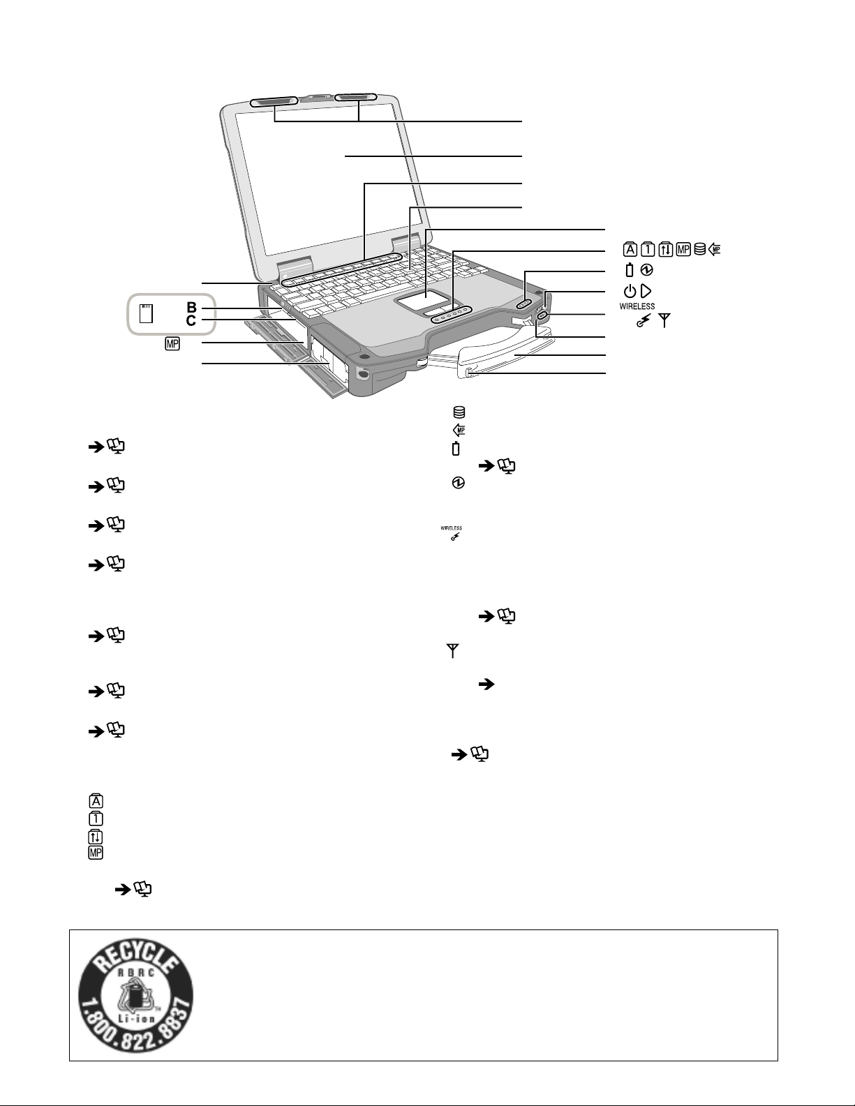
2 Names and Functions of Part
A
EX
PC
D
E
F
G
H
I
J
K
K
L
K
M
N
O
A: Bluetooth Antenna
<Only for model with Bluetooth>
Reference Manual “Bluetooth”
B: ExpressCard Slot
Reference Manual “PC Card / ExpressCard”
C: PC Card Slot
Reference Manual “PC Card / ExpressCard”
D: Multimedia Pocket
Reference Manual “Multimedia Pocket”
E: Battery Pack
F: Wireless LAN Antenna
<Only for model with wireless LAN>
Reference Manual “Wireless LAN”
G: LCD
<Only for model with touchscreen>
Reference Manual “Touchscreen”
H: Function Key
Reference Manual “Key Combinations”
I: Keyboard
J: Touch Pad
K: LED Indicator
: Caps lock
: Numeric key (NumLk)
: Scroll lock (ScrLk)
: Multimedia pocket device status or the second
battery status
Reference Manual “Multimedia Pocket”
“Battery Power”
: Hard disk drive status
: Power status of the multimedia pocket
: Battery status
Reference Manual “Battery Power”
: Power status
(Off: Power off/Hibernation, Green: Power on,
Blinking green: Standby)
: Wireless ready
This indicator lights when Wireless LAN, Bluetooth, and/or Wireless WAN are connected and
ready. It does not necessarily indicate the On/Off
condition of the wireless connection.
Reference Manual “Wireless LAN” “Blue-
tooth” “Wireless Switch Utility”
: Wireless WAN status
<Only for model with wireless WAN>
Refer to the instruction manual of the wireless
device
L: Power Switch
M: Wireless Switch
Reference Manual “Wireless Switch Utility”
N: Carrying Handle
O: Stylus Holder
A lithium ion battery that is recyclable powers the product you have purchased.
Please call 1-800-8-BATTERY for information on how to recycle this battery.
L’appareil que vous vous êtes procuré est alimenté par une batterie au lithium-ion.
Pour des renseignements sur le recyclage de la batterie, veuillez composer le
1-800-8-BATTERY.
Page 10
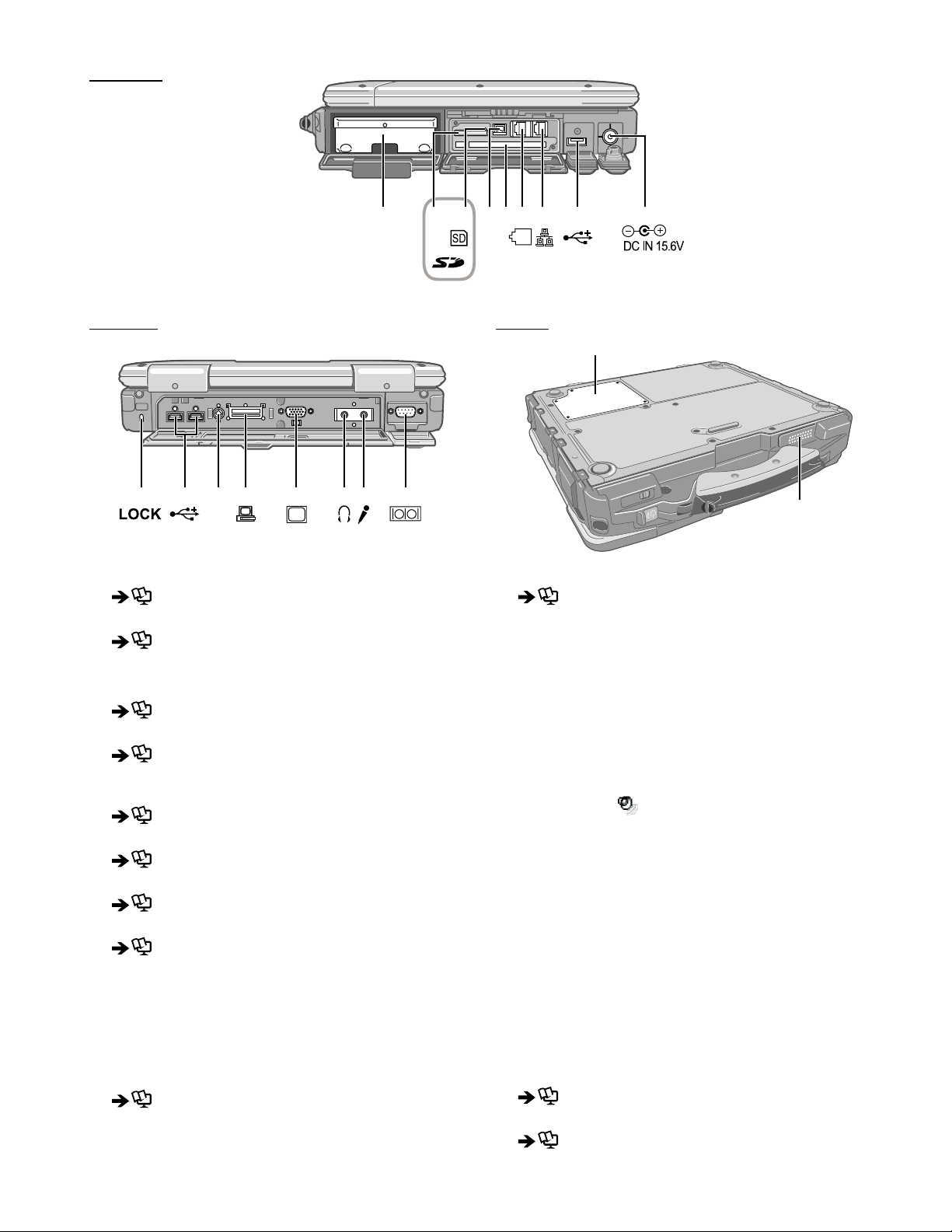
Right side
A B C D F E G H I
1394
Rear side Bottom
Q
J K M N O PLH
A: Hard Disk Drive
Reference Manual “Hard Disk Drive”
B: SD Memory Card Slot
Reference Manual “SD Memory Card”
C: SD Memory Card Indicator
(Blinking: During access)
Reference Manual “SD Memory Card”
D: IEEE 1394 Interface Connector
Reference Manual “IEEE 1394 Devices”
E: Smart Card Slot
<Only for model with Smart Card slot>
Reference Manual “Smart Card”
F: Modem Port
Reference Manual “Modem”
G: LAN Port
Reference Manual “LAN”
H: USB Port
Reference Manual “USB Devices”
I: DC-IN Jack
J: Security Lock
A Kensington cable can be connected.
For further information, read the manual that comes
with the cable.
K: Ext Antenna Connector
L: Expansion Bus Connector
Reference Manual “Port Replicator”
R
M: External Display Port
Reference Manual “External Display”
N: Headphone Jack
You can connect headphones or ampliÞ ed speakers.
When they are connected, audio from the internal
speakers is not heard.
O: Microphone Jack
A condenser microphone can be used. If other types
of microphones are used, audio input may not be possible, or malfunctions may occur as a result.
When recording in stereo using a stereo micro-
phone:
Double-click
tions] - [Properties], and add a check mark for [Recording], click [OK] - [Options] - [Advanced Controls]
- [Advanced], remove a check mark for [Mono Microphone], and then click [Close].
When using a monaural microphone with a 2-termi-
nal plug:
With the settings outlined above, only audio on the
left track will be recorded.
When monitoring the microphone audio using head-
phones, sounds on the left track cannot be heard,
regardless of the above settings. This is a result of
the computer’s speciÞ cations, and is not a malfunction.
P: Serial Port
Q: RAM Module Slot
Reference Manual “RAM Module”
R: Speaker
Reference Manual “Key Combinations”
in the notiÞ cation area, click [Op-
Page 11

(
)
L
T
p
r
B
g
A
k
T
r
r
s
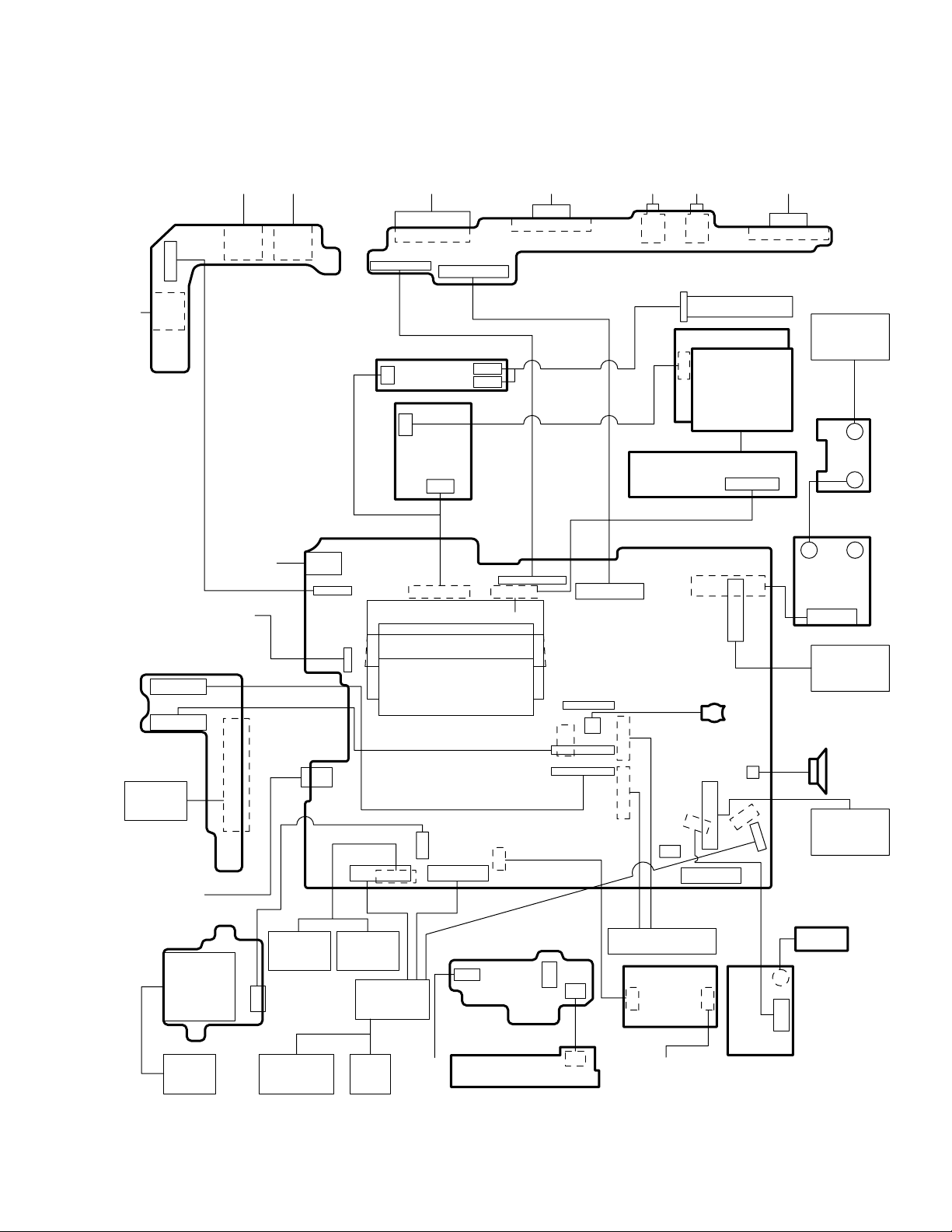
3 Block Diagram
4-1
eake
S
Headphone
Ext. MIC
Flat Pad
EC/KBC
(M306KA)
17Mbytes/sec
infineon
TPM 1.2
SMSC
Super I/O
SIO10N268
Tou ch
Screen
Wireless cinfig CN
Internal USB1.1
GPS
RJ11
DDR2 SDRAM
64bit BUS 1.8V 533MHz
DRAM
Internal
2GB
4.2Gbytes/sec
Interface
Graphics
HDA
Sound
STAC9200
MDC1.5
Data Modem
C Lin
2GB
DDR2 SDRAM
SD Card
IEEE1394
PCMCIA
R5C842
PC CARD TYPE II
nd
TYPE II
2
antenna
133Mbytes/sec
RJ45
SO-DIMM Memory
NNC1C000
88E8055-A3-
PCI
Marvell Yucon Ultra
e
Brid
AC-link
Interface
1.5V
INTEL
Interface
IDE
Interface
Interface
PATA
Buffer
Wireless LAN
34945ABG
802.11 A/B/G
4.2Gbytes/sec
64bit BUS 1.8V 533MHz
INTE
(1.05 )
DMI
Interface
1Gbytes/sec x2
DMI
HDD
8M
SPI
BIOS
SATA
(1.5Gb/s)
ExpressCARD
Bridge
PCI Expres
LPC
Bridge
USB 2.0
Interface
AMP
SO-DIMM Memory
1.05V
5.3Gbytes/sec
Yon ah DC
2MB L2 Cache
1.66GHz, FSB 667MHz
Battery Charger
HDD
Heate
Pack
Li-Ion
Battery
Pack
Li-Ion
Battery
LED
BKL
Int. K
KBD
PS/2
Mouse
KB& Mouse
Smart Card (new)
Parallel
(PortRep.)
Buffe
Serial
Serial
(PortRep)
L2400
Intel Core
Duo processor
CF-30
Block Diagram
LCD
1000nit
13.3” XGA
CR
PATA
MP
80GB 2.5”
SATA HDD
HUB
1.1/2.0
USB1.1
Blue-tooth
Finger Print
Internal USB1.1
Page 12
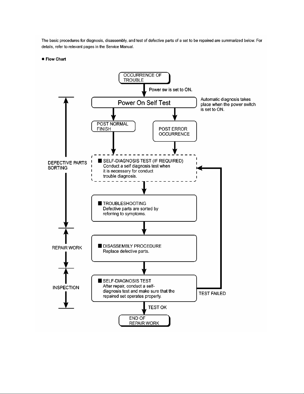
4 Diagnosis Procedure
4-1
4.1. Basic Procedures
Page 13
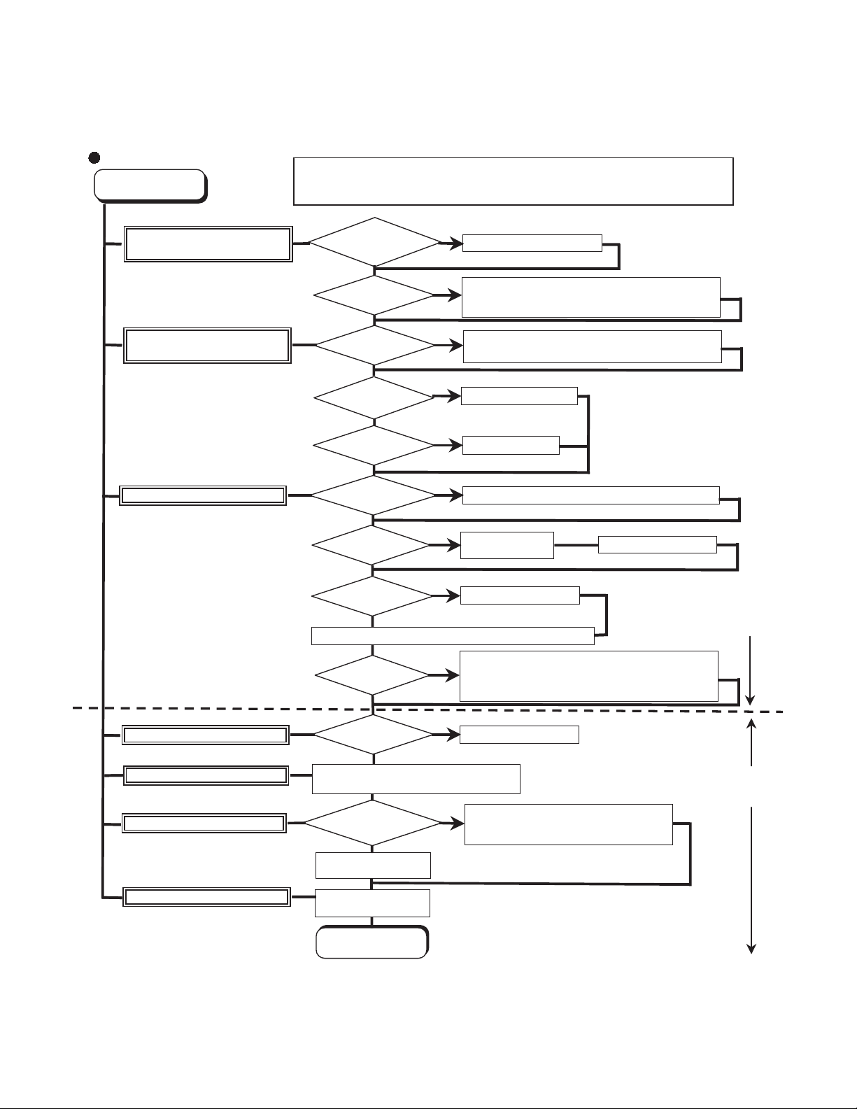
4.2. Troubleshooting
f
k
4-2
Please take note of the following two points with regard to troubleshooting:
1. Know-how of diagnosis upon occurrence of heavy troubles, e.g. Set cannot be turned ON , Set fails to start , No display on
screen , etc.
2. Explanation of each trouble, mainly symptom of trouble in operation.
Flow Chart
START
START
Pay attention to the following points when in pursuit of the cause of a troubleshooting.
1. Peripheral apparatus connected with the set should all be removed before operation check.
2. Make sure that cables, boards, etc. are not coming off, and recheck the contact condition.
Set cannot be supplied with current.
Power lamp fails to light up.
Dark display on screen.
Screen fails to display.
Failure in starting
Return set-up utility setpoint to the state of delivery from factory .
Not displayed properly on screen.
Some or all keys cannot be input.
Make sure of contact of K/B connector in use.
Replace keyboard or main board.
CD CALL not practicable.
Starts but operates unstably.
Reinstall HDD.
Replace main board.
AC
Adaptor/Battery
Output voltage
Power lamp
check
Inverter board
LCD back
light lighting
YES
LCD unit
check
OK
BIOS operation
chec
Result of
POST
Set-up utility
starting
OK
HDD access
YES
Main board
check
OK
Trouble
symptoms on some
of CD
YES
Replace main board.
OK
YES
OK
YES
OK
NO
NG
NO
NG
NO
NG
NG
NO
NG
NO
NG
Replace AC Adaptor/Battery
Check contact condition of power input terminal. Replace i
defective.
Check Power SW. Replace if defective.
Replace inverter board.
Check inverter cable continuity. Replace if defective
Replace LCD back light.
Replace LCD unit.
Replace main board (Check fuse at power source).
Refer to POST
error code table.
Replace main board.
Check HDD cable connection and continuity.
Replace if defective.
Replace HDD & Reinstall.
Replace main board.
Replace main board
Check if there are any flaws on CD media. Since
flaws may appear on specific media, CD media
can be defective.
Replace main board.
Heavy trouble e.g.,
Set cannot be turned
ON , Set fails to start ,
No display on
screen , etc.
Each kind of
trouble in
operation.
START
END
Page 14
5 Power-On Self Test (Boot Check)
5-1
Outline of POST
The set has a boot check function called POST (Power-On Self Test) in it.
The condition of the main body is diagnosed by checking
Start .............Test begins automatically when power switch is set to ON.
Normal finish .....After memory checking, a beep sound is issued once and the set is placed into automatic stop.
Note: If no error occurs, nothing is displayed. (No display of OK, etc.)
Error Diagnosis by Checking Beep Signal Sound
The beep sound is as follows:
(Length of bar shows length of sound.)
beep sound or error code.
(1 (long sound) -2-3-4)
= long sound (about 0.4 sec.),
Table of errors classified by beep sounds
Diagnosis Beep signal sound Error message
Main board
(Note) A beep sound is also issued in case of other I/O trouble.
1(long sound)-2 BIOS ROM error
1-2-2-3
1-3-1-1
1-3-1-3
1-3-4-1
1-3-4-3
1-4-1-1
= short sound (about 0.2 sec.), Length between sounds is about 0.1 sec.
BIOS ROM error
RAM error
Keyboard controller error
RAM error
RAM error
RAM error
BIOS ROM error2-1-2-3
Occurrence of unexpected offering2-2-3-1
Page 15

6 List of Error Codes <Only when the port replicator is connected>
6-1
The following is a list of the messages that BIOS can display. Most of them occur during
POST. Some of them display information about a hardware device, e.g., the amount of memory
installed. Others may indicate a problem with a device, such as the way it has been configured.
Following the list are explanations of the messages and remedies for reported problems.
If your system displays one of except the messages marked below with an asterisk (*), write
down the message and contact Panasonic Technical Support. If your system fails after you
make changes in the Setup menus, reset the computer, enter Setup and install Setup defaults
or correct the error.
0200 Failure Fixed Disk
Fixed disk in not working or not configured properly. Check to see if fixed disk is attached
properly. Run Setup. Find out if the fixed-disk type is correctly identified.
0210 Stuck key
Stuck key on keyboard.
0211 Keyboard error
Keyboard not working.
0212 Keyboard Controller Failed
Keyboard controller failed test. May require replacing keyboard controller.
0213 Keyboard locked - Unlock key switch
Unlock the system to proceed.
0230 System RAM Failed at offset : nnnn
System RAM failed at offset nnnn of in the 64k block at which the error was detected.
0231 Shadow RAM Failed at offset : nnnn
Shadow RAM failed at offset nnnn of the 64k block at which the error was detected.
0232 Extended RAM Failed at offset : nnnn
Extended memory not working or not configured properly at offset nnnn.
0250 System battery is dead - Replace and run SETUP
The CMOS clock battery indicator shows the battery is dead. Replace the battery and run Setup
to reconfigure the system.
*0251 System CMOS checksum bad - Default configuration used
System CMOS has been corrupted or modified incorrectly, perhaps by an application program
that changes data stored in CMOS. The BIOS installed Default SETUP Values. If you do not
want these values, enter Setup and enter your own values. If the error persists, check the system
battery or contact Panasonic Technical Support.
0260 System timer error
The timer test failed. Requires repair of system board.
0270 Real time clock error
Real-time clock fails BIOS test. May require board repair.
*0280 Previous boot incomplete - Default configuration used
Previous POST did not complete successfully. POST loads default values and offers to run
Setup. If the failure was caused by incorrect values and they are not corrected, the next boot
will likely fail. On systems with control of wait states, improper Setup settings can also termi-
nate POST and cause this error on the next boot. Run Setup and verify that the wait-state
configuration is correct. This error is cleared the next time the system is booted.
0281 Memory Size found by POST differed from EISA CMOS
Memory size found by POST differed from EISA CMOS.
Page 16

02D0 System cache error - Cache disabled
6-2
Contact Panasonic Technical Support.
02F0: CPU ID:
CPU socket number for Multi-Processor error.
02F4: EISA CMOS not writable
ServerBIOS2 test error: Cannot write to EISA CMOS.
02F5: DMA Test Failed
ServerBIOS2 test error: Cannot write to extended DMA (Direct Memory Access) registers.
02F6: Software NMI Failed
ServerBIOS2 test error: Cannot generate software NMI (Non-Maskable Interrupt).
02F7: Fail - Safe Timer NMI Failed
ServerBIOS2 test error: Fail-Safe Timer takes too long.
device address Conflict
Address conflict for specified device.
Allocation Error for: device
Run ISA or EISA Configuration Utility to resolve resource conflict for the specified device.
Failing Bits : nnnn
The hex number nnnn is a map of the bits at the RAM address which failed the memory test.
Each 1 (one) in the map indicates a failed bit. See error 230,231 or 232 for offset address of the
failure in System, Extended or Shadow memory.
Invalid System Configuration Data
Problem with NVRAM (CMOS) data.
I/O device IRQ conflict
I/O device IRQ conflict error.
Operating System not found
Operating system cannot be located on either drive A: or drive C:. Enter Setup and see if fixed
disk and drive A: are properly identified.
Parity Check 1 nnnn
Parity error found in the system bus. BIOS attempts to locate the address and display it on the
screen. If it cannot locate the address, it displays ????. Parity is a method for checking errors
in binary data. A parity error indicates that some data has been corrupted.
Parity Check 2 nnnn
Parity error found in the I/O bus. BIOS attempts to locate the address and display it on the
screen. If it cannot locate the address, it displays ????.
Press <F1> to resume, <F2> to Setup
Displayed after any recoverable error message. Press <F1> to start the boot process or <F2> to
enter a Setup and change the settings. Write down and follow the information shown on the
screen.
Troubleshooting
Page 17
7 Self Diagnosis Test
7-1
As for the self-diagnosis test(PC-Diagnostic utility) to use this model, a standard test and the
enhancing test by the module of the main body building in are possible.
Notes
1. Beginning of self-diagnosis test
1-1. Setting of content of setup
The power supply of the computer is turned on.
1.
" F2 " is pushed on the screen of "Panasonic" while " press <F2 to enter Setup> " is displayed.
2.
The setup utility starts and then takes notes of the content of the BIOS setup of present set.
3.
" F9 " is pushed, " Yes" is selected on the screen of " Is the default value loaded? ", and " Enter"
4.
is pushed.
" F10 " is pushed.
5.
" Yes" is selected on the screen of the setup confirmation, and " Enter" is pushed.
6.
The computer starts automatically.
7.
Attention
If the device which can be set is set to "Invalidity" by "Advanced" or "Security" menu, becomes an
error by "PC-Diagnostic utility".
(It is judged that the device which can be set to "Invalidity" by "Main" menu such as "Flat pad" is
normal if the controller operates normally though sets to "Invalidity" by the setup. )
In the model with built-in DVD of the USB connection, even if DVD is normal, becomes an error if
legacy USB is set to "Invalidity"
To skip BIOS password
Use <Ctrl>+<F10> key to skip BIOS password or authentication of fingerprint.
This key is only for entering DIAG mode. Not available to boot the computer.
If customer set "HDD Lock", the DIAG program cannot perform HDD test.
*This key is for service purpose only. Do not disclose this information to unrelated others.
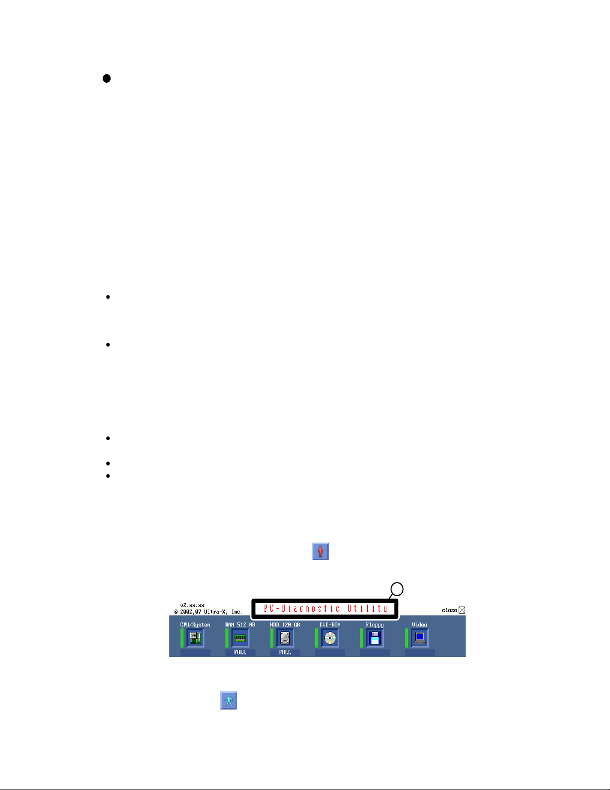
1-2. When you execute an automatic test
1.
"Ctrl" + "F7" is pushed while the "Panasonic" start screen is displayed after the computer is started.
2.
The test of all devices begins automatically by "PC-Diagnostic utility"’s starting.
Attention
It is a test which the customer who bought PC can execute. (As for HDD, the enhancing test is also
possible.)
A flat pad does not work for a while after starting "PC-Diagnostic utility".
The movement of a flat pad might become abnormal If after RAM begins from the CPU/System
test, a flat pad will be operated in about 30 seconds. In that case,restarts pushing"Alt" + "Ctrl" +
"Del" key. Or, please start "PC-Diagnostic utility" again after doing the power supply switch in the
slide, and turning off the power supply.
1-3. When you execute the enhancing test
Please let me discontinue diagnosing clicking to end an automatic test.
1.
Please click on the character of "D" "PC-Diagnostic utility" on the screen while pushing both of right
2.
"Shift" and left "Shift" keys.
D
All devices which can select the enhancing test make the setting of the enhancing test possible.
3.
The district device is made"FULL" display (enhancing test).
4.
The test begins clicking .
5.
*Please refer to item 4 for the error result of each test and the division of the breakdown part.
Page 18
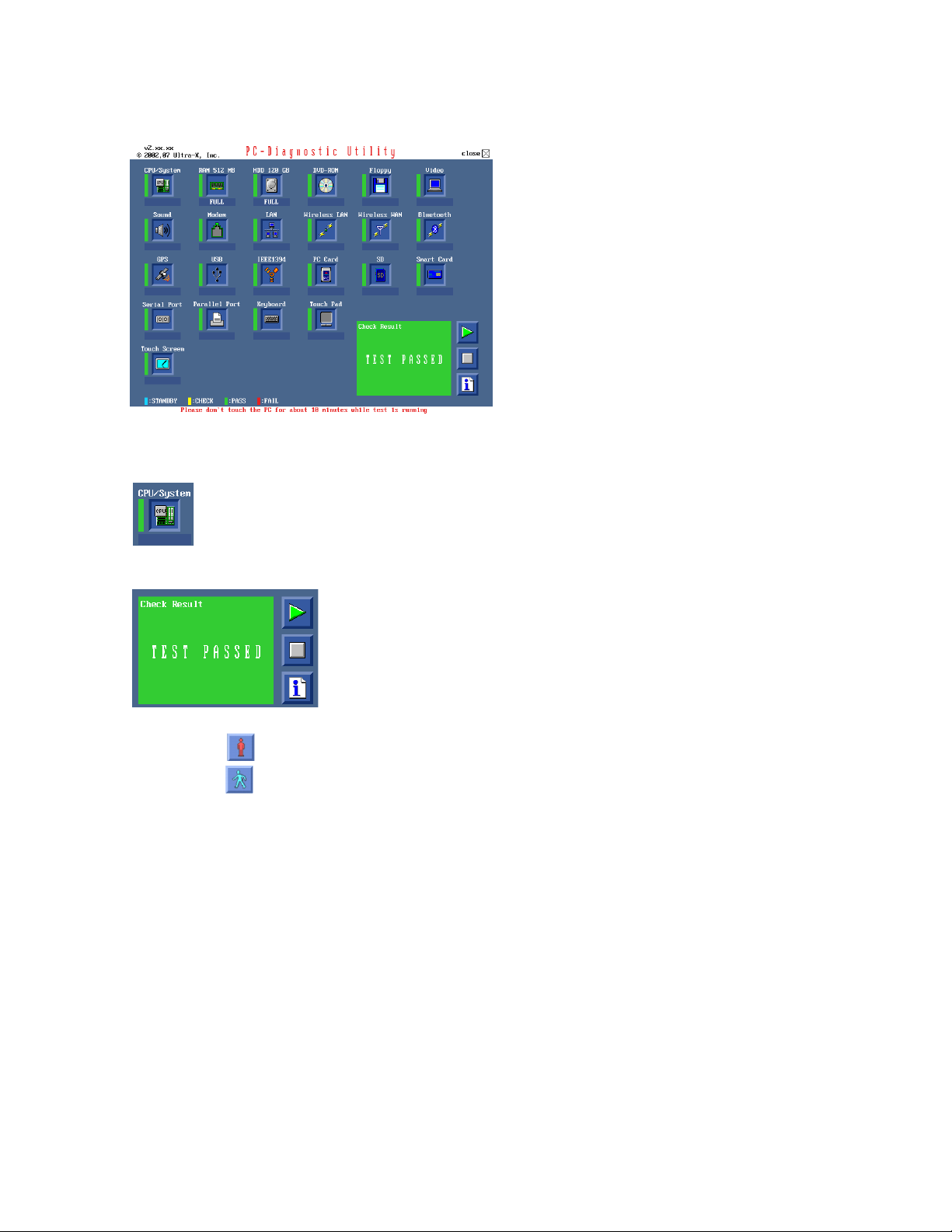
2. Operation of PC-Diagnostic Utility
7-2
-Only the device which can be inspected on the entire screen is displayed.
-The item does not appear when the device of wireless LAN etc. is not physically connected.
-The movement of the item must use an arrow key or a flat pad.
-As for the device under the diagnosis, blue and yellow are alternately displayed at the left of the icon.
- The diagnosis result of the device greens at the left of the icon when it is normal, and becomes red when
abnormal.
-When the test of all devices ends, the test result is displayed under the right of the screen.
-Please click while diagnosing when being stop on the way by the time the test of all devices ends.
-Please click when you restart "PC-Diagnostic utility".
*Each device is tested from the beginning, and it is not possible to restart on the way.
Page 19
2-1. Selection of tested device
7-3
-To test only a specific device, "Test" and "Do not test" of each device can be selected.
-The device which can select the enhancing test changes in order of "The standard is tested" and "Do not
test" whenever the device icon is clicked.
Start the standard test
Please begin testing clicking if the selection of the tested device ends.
Do not test
2-2. "PC-Diagnostic utility" End method
When of "Close" on the right of the screen is clicked, the computer reactivates automatically. Or, the
power supply switch is done in the slide and the power supply is turned off.
2-3. The content of the setup is returned to the setting of the user
Turned on the computer.
1.
"F2" is pushed on the screen while "Press<F2>to enter Setup" is displayed of "Panasonic".
2.
Push "F10", and on the screen of "Is the change in the setting preserved and do end?"and then "Yes"
3.
is selected, and "Enter" is pushed.
The computer reactivates automatically.
4.
The end option is chosen by the start menu, and the power supply of the computer is turned off.
5.
Standard at test time
All devices other than RAM and HDD
RAM standard test
HDD standard test
HDD enhancing test (60GB)
about 1 minute
1 - 2 minutes
2 - 3 minutes
about 40 minutes
Ex.The standard when the standard <all device> is tested becomes 1+2+3=6 minutes.
There is greatly a difference from RAM test when the memory is increased according to the performance of the memory occasionally.
Moreover, when the main body of PC under the test is a high temperature, it occasionally takes time.
There is greatly a difference from HDD according to the performance of the drive occasionally.
Page 20
7.1. Test Item and Division of trouble
7-4
Test item Stanard
CPU /
SYSTEM
RAM All memory space is tested in a spe-
HDD The record area frequently accessed
MODEM It is confirmed not to find abnormality
Wireless
LAN
Enhancing
Content of standard test Content of enhancing test
CPU is shifted to protected mode, and
"Violation of the paging", "Operation of
the violation of a privileged instruction", and DMA, INT, TIMER, and the
RTC operation are confirmed.
cial memory access pattern based on
"R.S.T . technology".
with Microsoft Windows XP to test in
about two minutes regardless of
points of HDD is emphatically tested.
in the AC97 modem controller.
It is confirmed not to find abnormality
in the Wireless LAN modem controller.
Place with possibili-
ty of breakdown
CPU /
Main board
Memory / Mainboard
All record area is tested. HDD /
Mainboard /
Cable /
Connector
MODEM/ Mainboard
Wireless LAN
board /
Connector /
Mainboard
Sound
USB It is confirmed not to find abnormality
LAN It is confirmed not to find abnormality
PC Card It is confirmed not to find abnormality
SD It is confirmed not to find abnormality
Keyboard It is confirmed not to find abnormality
*5
in the USB controller.
*1
in the LAN controller.
*2
in the CardBus controller.
in the SD controller.
*3
in keyboard controller’s keyboard interface.
It is confirmed not to find abnormality in the wiring between the USB controller and
the connector by confirming
the connection of the USB
equipment connected with the
USB connector.
It is confirmed not to find abnormality in the wiring between the controller and the
connector by connecting to
HUB with LAN cable.
The key is actually input, and
the operation is displayed on
the screen.
Mainboard /
Connector
Mainboard /
Connector
Mainboard
Mainboard
Mainboard /
Keyboard
Touch Pad
DVD-ROM
Whether keyboard controller’s mouse
*4
interface operates normally is confirmed.
*6
The drive is normally reset, and it is
accessible is confirmed.
The operation is actually displayed on the screen by operating the touch pad.
It is confirmed to be able to
read media normally.
Mainboard /
Touch Pad
Mainboard /
Touch Pad
Page 21
Test Item
7-5
Touch Screen
Standard Enhanced
Content of Standard Test Content of Extend Test
It is confirmed not to find
abnormality in the USB
connection of Touch Screen.
This test cannot find
abnormality of Touch Screen.
Perform Touch Screen
functionality practically.
Operator has to judge
PASS/FAIL with test result.
It is confirmed not to find
Bluetooth
abnormality in the connection
of Main board and Bluetooth
module.
It is confirmed not to find
Wireless WAN
abnormality in the connection
of Main board and Wireless
WAN module.
It is confirmed not to find
abnormality in the legacy FD
Floppy
drive.
This test cannot find
abnormality of mechanical
breakdown. (e.g.. Head, Motor)
It is confirmed not to find
abnormality in access to
Video
VRAM with VESA.
The PC which uses main
memory as VRAM may fail with
main memory failure.
It is confirmed not to find
GPS
abnormality in the connection
of Main board and GPS
It is confirmed not to find
IEEE1394
abnormality in the IEEE1394
controller.
It is confirmed not to find
Express Card
abnormality in the wiring
between Chipset and Express
Card.
It is confirmed not to find
Smart Card
abnormality in the Smart Card
controller.
It is confirmed not to find
abnormality of Super I/O
Serial Port *7
UART function.
This test cannot find lack of
wiring between Super I/O and
Serial Connector.
It is confirmed not to find
abnormality of Super I/O
Parallel Port *8
parallel function.
This test cannot find lack of
wiring between Super I/O and
Parallel Connector.
*1
Please connect the USB device with the port (USB connector) which wants to test before the tests.
*2
Please connect LAN port with LAN HUB with LAN cable before the tests.
The operator actually inputs the key, and the operator judges PASS/FAIL of the test.
*3
The operator actually operates the mouse, and the operator judges PASS/FAIL of the test.
*4
It is not abnormal though the sound is emitted from the speaker while testing.
*5
It is confirmed not to find
abnormality in the wiring
between Super I/O and Serial
Connector.
This test cannot find failure of
cable characteristic and device
problems.
It is confirmed not to find
abnormality in the wiring
between Super I/O and
Parallel Connector.
This test cannot find failure of
cable characteristic and device
problems.
When the test result is PASS, trouble is thought by not hearing of the sound under the test from
the speaker and the headphone by the wiring of the audio output system.
*6
Please set DVD/CD media in the drive before the tests.
*7 Please set a Special Loop Back Connector Tool at serial connector for Enhanced Test.
(This Connector Tool is same as the one used before.)
*8 Please set a Special Loop Back Connector Tool at parallel connector for Enhanced Test.
(This Connector Tools is same as the one used before.)
The place with possibility of
breakdown
Main board/
Touch Screen
Bluetooth cable
WWAN cable
FD Drive/
Main board (Super I/O)/
FDD cable
FDD connector
Main board
(Chipset, Graphic
Controller)/
Memory
GPS cable
Main board
(IEEE#394 Controller)
Main board (Chipset)/
Express Card Connector
Main board
(Smart Card Controller)
Main board (Super I/O)/
Serial Connector
Main board (Super I/O)/
Parallel Connector
Page 22
8 Wiring Connection Diagram
8-1
USB
PORT
USB
PORT
EXPANSION
BUS
EXTERNAL
DISPLAY
PORT
HEAD
PHONE
MICRO
PHONE
SERIAL
PORT
CN100
USB
PORT
CN103
LAN PORT
MP PCB
CN400
CN401
COMBO
DRIVE
IEEE1394
INTERFACE
CONNECTOR
CN301
CN102 CN101
USB PCB
DC-IN
CN402
PW LED
PCB
CN300
JK1
CN3
CN28
CN701
INVERTER PCB
CN201
TS PCB
CN27
CN20
DIMM MEMORY CARD
CN31
SW LED
PCB
HDD FPC
BATTERY
CN200
CN4
CN705 CN703
CN700
CN2
CN21
CN22
CN24
CN7CN8
PAD PCB
CN801
CN17
I/O PCB
CN15
CN5
CN800
MAIN PCB
CN12
CN19
CN6
CN802
JK701 JK700
CN1
CN13
CN14
KEYBOARD
MDC
MODEM
BACK LIGHT
TOUCH SCREEN
LCD
CN37
CN11
RTC
BATTERY
CN10
CN25
CN18
CN29
CN30
J2J1
CN1
CN26
CN9
CN702
ANTENNA
PCB
CN1
CN2
EXT ANT.
PCB
W-LAN
MODULE
EXPRESS
CARD
SPEAKER
PCMCIA
CARD
BT PCB
JK1
SD
CARD
MAIN
BATTERY
HDD
TOUCH
PAD
LED PCB
CN901
MODEM
PORT
CN1
GPS PCB
Page 23
9 Disassembly/Reassembly
Note:
Power off the computer. Do not shut down to the Suspend or hibernation mode.
Do not add peripherals while the computer is in the Suspend or hibernation mode; abnormal operation may result.
9.1. Disassembly Instructions
9.1.1. Preparation
Before disassembling, be sure to make the following preparations.
• Shut down Windows and turn off the power.
• Disconnect the AC adaptor.
• Remove the optional DIMM memory card and PCMCIA card if
they are connected.
• Remove other devices if they are connected.
Attention:
• Please execute writing BIOS ID when you exchange the Main
Board.
• Parts (Sheet and rubber) etc. related various the Conductive
Cloth and Heat Spreader cannot be recycled. Use new parts.
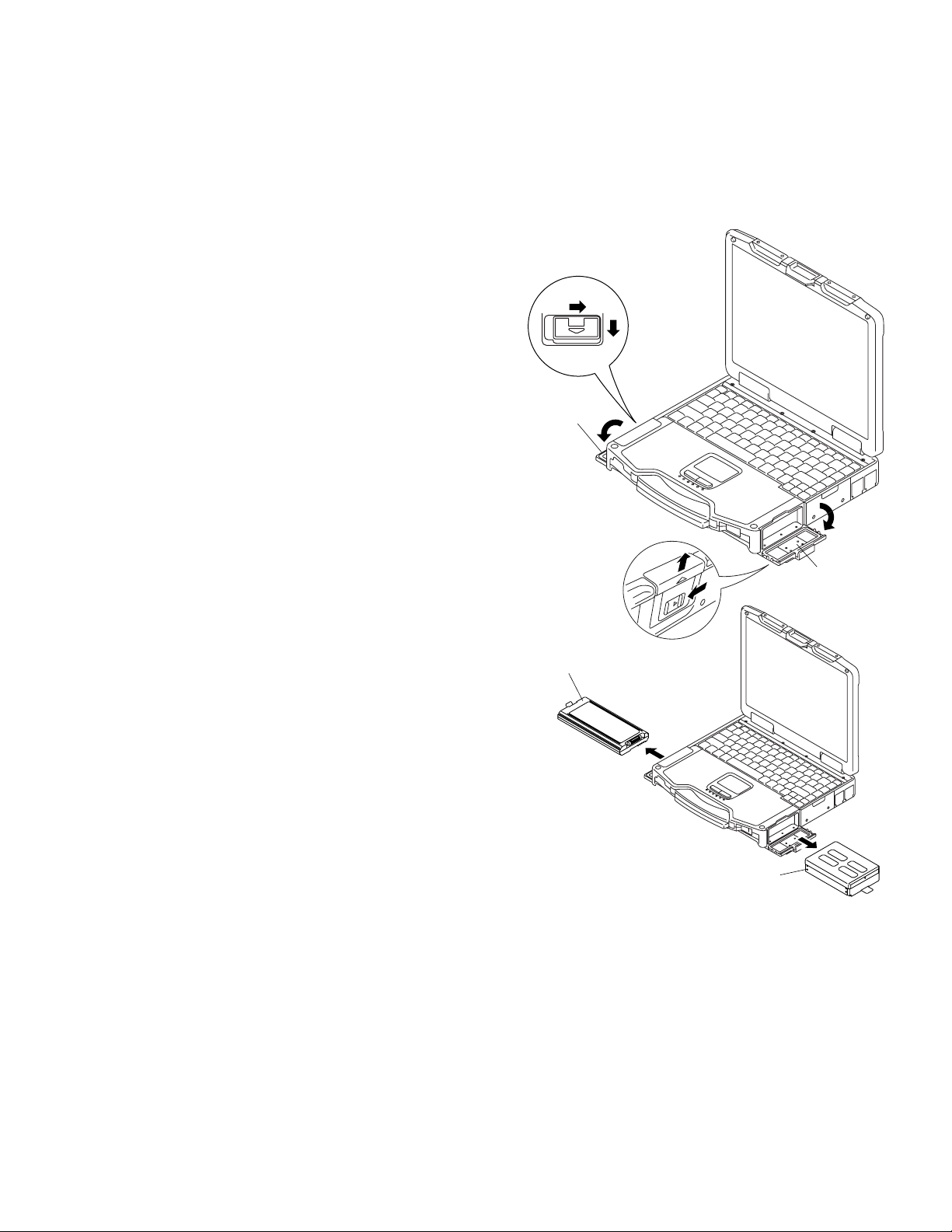
9.1.2. Removing the Battery Pack and HDD
Pack
Battery
Cover
HDD Cover
Battery Pack
1. Open the Battery Cover.
2. Remove the Battery Pack.
3. Open the HDD Cover.
4. Remove the HDD Pack.
HDD Pack
9-1
Page 24
9.1.3. Removing the HDD
HDD FPC
HDD
Heater Sheet
Sheet
Heater
Sheet
<K1-17>
<K1-17>
Ta b
1. Remove the Screw. <K1-16>
2. Remove the 4 Screws. <K1-17>
3. Release the 2 Tabs, and remove the HDD U Case Ass'y
and the HDD L Case Ass'y.
4. Remove the HDD Dumper Ass'y.
5. Remove the 2 Sheets.
6. Remove the Heater and the Heater Sheet.
7. Remove the HDD FPC.
Screws <K1-16>: DFHE5025XA
Screws <K1-17>: DRQT2+E8FKL
HDD U Case Ass’y
<K1-16>
Ta b
HDD L
Case Ass’y
HDD
Damper
Ass’y
9.1.4. Removing the KB Cover, Hinge
Cover L, Hinge Cover R and Keyboard
<N5>
<N5>
<N5>
<N5>
KB Cover
1. Remove the 4 Screws <N5>, and remove the KB Cover.
2. Remove the 2 Screws <N2> and the 4 Screws <N5>, and
remove the Hinge Cover L,R.
3. Remove the Keyboard.
Screws <N2>: DRHM5054XA
Screws <N5>: DRQT26+D4FKL
<N5>
<N5>
Bluetooth PCB
<N2>
Hinge Cover L
<N5>
Hinge
Cover R
Keyboard
<N5>
<N2>
9-2
Page 25
9.1.5. Removing the KB Cable Cover and
LCD Cable Cover
9.1.6. Removing the GPS PCB and Bluetooth PCB
<N4>
<N4>
<N4>
<N4>
KB Cable Cover
<N4>
LCD
Cable Cover
<N4>
<N4>
LCD
Cable Plate
Connector
(CN14)
Connector
(CN13)
Keyboard
<N4>
<N4>
to Connector
(CN13)
<N4>
to Connector
(CN14)
1. Remove the 3 Screws <N4>.
2. Remove the LCD Cable Cover.
3. Remove the LCD Cable Plate.
4. Remove the 7 Screws <N4>.
5. Remove the KB Cable Cover.
6. Disconnect the 2 Cable from the 2 Connectors (CN13,
CN14).
7. Remove the Keyboard.
<N12>
<N12>
GPS PCB
<N11>
to Connector
(CN25)
<N12>
GPS BT Angle
<N12>
<N11>
Connector(CN25)
Bluetooth
PCB
1. Disconnect the Cable from the Connector. (CN25)
2. Remove the 4 Screws. <N12>
3. Remove the 2 Screws. <N11>
4. Remove the Bluetooth PCB, GPS BT Angle and GPS PCB.
Screws <N11>: DFHE5025XA
Screws <N12>: DXQT2+F3FNL
Screws <N4>: DRQT26+D3FKL
9-3
Page 26

9.1.7. Removing the DIMM Cover and Bottom Cover
9.1.8. Removing the USB PCB and Antenna
PCB
DIMM Cover
DIMM Stopper Base
DIMM Heat Plate
DIMM Memory Card
<N6>
<N8>
Bottom Cover
<N6>
<N6>
<N1>
<N8>
<N6>
<N6>
<N1>
<N1>
<N5>
<N1>
<N5>
<N6>
<N8>
<N6>
<N1>
<N6>
<N6>
<N8>
<N6>
<N6>
<N6>
<N8>
USB PCB
Antenna PCB
Antenna Cable
(White)
Antenna Cable
(White)
Connector
(CN100)
Tape
<N5>
Connector Cover
<N3>
<N3>
1. Remove the 5 Screws. <N1>
2. Remove the DIMM Cover.
3. Remove the 2 Screws. <N5>
4. Remove the DIMM Stopper Base.
5. Remove the DIMM Heat Plate.
6. Remove the DIMM memory card.
7. Remove the 6 Screws. <N8>
8. Remove the 13 Screws. <N6>
9. Remove the Bottom Cover.
1. Remove the Screw. <N5>
2. Disconnect the Cable from the Connector. (CN100)
3. Remove the Tape.
4. Remove the USB PCB.
5. Open the Connector Cover.
6. Remove the 2 Screws. <N3>
7. Remove the 2 white Cables and remove the Antenna PCB.
Screws <N3>: DRQT2+G6FKL
Screws <N5>: DRQT26+D4FKL
Screws <N1>: DRHM0002ZA
Screws <N5>: DRQT26+D4FKL
Screws <N6>: DRQT26+E4FKL
Screws <N8>: DRSB3+8FKL
9-4
Page 27

9.1.9. Removing the FPC HDD BAT
9.1.10. Removing the PAD PCB
to Connector (CN8)
to Connector (CN7)
FPC HDD BAT
<N4>
<N4>
HDD Cable Cover
Pad Protect
Sheet
Connector
(CN8)
Connector
(CN7)
Pad PCB
<N4>
<N4>
<N4>
<N16>
to Connector (CN9)
to Connector (CN800)
Tape
Antenna Cable Sheet
to Connector (CN26)
Connector(CN10)
Connector(CN26)
Tape
Connector(CN9)
Connector (CN800)
1. Remove the 5 Screws. <N4>
2. Remove the HDD Cable Cover.
3. Remove the Antenna Cable Sheet.
4. Remove the 2 Tapes.
5. Disconnect the 2 Cables from the 2 Connectors.
(CN10,CN26)
6. Remove the Tape.
7. Disconnect the Cable from the Connector. (CN9)
8. Remove the Pad Protect Sheet.
9. Disconnect the Cable from the Connector. (CN800)
10. Disconnect the 2 Cables from the 2 Connectors. (CN7,CN8)
11. Remove the Screw. <N16>
12. Remove the FPC HDD BATT.
Screws <N4>: DRQT26+D3FKL
Screws <N16>: DRQT26+E5FKL
TP PCB Screw Sheet
Tape
<N4>
<N4>
Connector
(CN801)
Pad PCB
Connector
(CN802)
1. Remove the Tape and disconnect the Cable from the Connector. (CN801)
2. Disconnect the Cable from the Connector. (CN802)
3. Remove the TP PCB Screw Sheet.
4. Remove the 2 Screws. <N4>
5. Remove the PAD PCB.
Screws <N4>: DRQT26+D3FKL
9.1.11. Removing the Main PCB
TOP Screw Sheet
<N7>
Connector
(CN17)
Connector
(CN27)
1. Remove the TOP Screw Sheet.
2. Remove the Screw. <N7>
3. Disconnect the 2 Cables from the 2 Connectors.
(CN17,CN27)
9-5
Page 28

Connector
(CN31)
Pet Tape
<N16>
<N18>
<N16>
<N16>
Connector(CN700)
<N16>
to Connector(CN700)
to Connector(CN701)
<N16>
<N16>
Main Chasis
Connector(CN701)
(CN400,CN401)
11. Remove the 2 Screws. <N5>
12. Remove the 2 Screws. <N21>
13. Remove the MP Guide.
14. Remove the MP PCB.
15. Remove the Coin Battery Cushion.
16. Disconnect the Cable from the Connector. (CN19)
17. Remove the Coin Battery.
18. Remove the Tape.
19. Disconnect the 2 Cables from the 2 Connectors.
(CN4,CN11)
<N17>
ICH Plate
<N5>
<N5>
<N17>
<N5>
<N17>
<N5>
<N11>
<N11>
Tape
<N11>
Modem
Cable Sheet
<N5>
<N5>
Modem
LAN Case
4. Remove the 6 Screws. <N16>
5. Remove the Screw. <N18>
6. Disconnect the 2 Cables from the 2 Connectors.
(CN700,CN701)
7. Remove the Pet Tape and disconnect the Cable from the
Connector. (CN31)
8. Remove the Main chasis.
<N21>
<N21>
MP Guide
<N5>
Coin Battery
Cushion
Coin Battery
Connector
(CN4)
Connector
(CN401)
<N5>
Tape
Connector
(CN400)
MP PCB
Connector
(J2)
<N11>
1394 Sheet
<N5>
Modem
Cable
MDC
<N5>
<N5>
<N5>
20. Remove the 3 Screws <N17> and the Screw. <N11>
21. Remove the ICH Plate.
22. Remove the 2 Modem Cable Sheets.
23. Remove the 2 Screws. <N5>
24. Remove the Modem LAN Case.
25. Remove the 1394 Sheet.
26. Remove the 2 Screws. <N11>
27. Remove the Tape.
28. Disconnect the Cable from the Connector (J2) and remove
the MDC.
29. Remove the Modem Cable.
30. Remove the 7 Screws. <N5>
31. Remove the Screw. <N11>
32. Remove the Main PCB.
Connector
(CN11)
Connector
(CN19)
9. Remove the Tape.
10. Disconnect the 2 Cables from the 2 Connectors.
Screws <N5>: DRQT26+D4FKL
Screws <N7>: DRSB26+10HKL
Screws <N11>: DFHE5025XA
Screws <N16>: DRQT26+E5FKL
Screws <N17>: DRQT26+E6FKL
Screws <N18>: DRSB26+8FKL
Screws <N21>: DXQT2+E12FNL
9-6
Page 29

9.1.12. Removing the SD PCB, Express Card
and PCMCIA Card
<N22>
<N22>
<N22>
<N22>
<N22>
<N22>
<N22>
Express Card
<N22>
9.1.13. Removing the I/O PCB
Connector
(CN701)
Connector
(CN700)
Connector Cover
I/O PCB
<N15>
<N14>
Lib Cover
<N15>
<N14>
PCMCIA Card
1. Remove the 2 Screws. <N5>
2. Remove the SD PCB.
3. Remove the 4 Screws. <N22>
4. Remove the Express Card.
5. Remove the 4 Screws. <N22>
6. Remove the PCMCIA Card.
Screws <N5>: DRQT26+D4FKL
Screws <N22>: DXQT2+G4FNL
<N5>
<N5>
SD PCB
1. Open the Connector Cover and Lid Cover.
2. Remove the 4 Screws. <N14>
3. Remove the 4 Screws. <N15>
4. Remove the I/O PCB.
Screws <N14>: DFHE5058ZB
Screws <N15>: DRHM5104ZA
9-7
Page 30

9.1.14. Removing the Palm Top Cover Sheet,
Palm Top Cover, Touch Pad Adhesion Seat, Touch Pad, Touch Pad SW
Knob, LED PCB and SW LED PCB
Palm Top Cover Sheet
<N4>
<N4>
<N4>
<N4>
9.1.15. Removing the Handle and Power SW
<K2-41>
Handle Base L
Handle Base R
<K2-41>
Handle
LED PCB
Touch Pad
SW Knob In
Hole 1
Touch Pad Adhesion Seat
Touch Pad
Touch Pad SW Knob
Hole 2
Palm Top Cover
<N5>
PW LED
PCB
PW LED Sheet
SW LED
PCB
WM SW
<K2-42>
Power
SW
1. Remove the 2 Screws <K2-41>, and remove the Handle
Base L and R.
2. Remove the Handle.
3. Remove the 2 Screws. <K2-42>
4. Remove the WM SW and Power SW.
Screws <K2-41>: DRSN4+6FKLT
Screws <K2-42>: DXQT26+D4NLT
1. Remove the Palm Top Cover sheet.
2. Remove the 5 Screws <N4>, and remove the Palm Top
Cover.
3. Remove the Touch Pad Adhesion seat.
4. Remove the Touch Pad.
5. Remove the Touch Pad SW knob and Touch Pad SW Knob
in.
6. Remove the LED PCB.
7. Remove the PW LED Sheet.
8. Remove the Screw <N5>, and remove the SW LCD PCB.
Screws <N4>: DRQT26+D3FKL
Screws <N5>: DRQT26+D4FKL
9-8
Page 31

9.1.16. Removing the Display Unit
Display Unit
<N9>
<N9>
<N9>
<N9>
<N10>
<N10>
9.1.17. Removing the LCD Rear Cabinet,
Hinge L and R
left LCD Cover
Side Cover
<N7>
Wireless Antenna
Corner Cover
<N7>
<N7>
LCD Latch
<N7>
<N7>
<N13>
<N7>
<K9-1-4>
Hinge L
<N7>
<N7>
LCD Rear Cabinet
<N7>
<N13>
<N7>
<N7>
<N7>
right LCD Cover
Side Cover
Wireless Antenna
Corner Cover
<K9-1-4>
Hinge R
1. Remove the 2 Screws <N10> and the 4 Screws <N9>.
2. Remove the Display Unit.
Screws <N9>: DRYN4+J10FKL
Screws <N10>: DXSB4+15FNLB
LCD Front Cabinet
1. Remove the 4 Screws. <N7>
2. Remove the 2 Wireless Antenna Corner Covers.
3. Remove the 4 Screws <N7> and 2 Screws. <N13>
4. Remove the left and right LCD Cover Side Covers.
5. Remove the 4 Screws. <N7>
6. Remove the LCD Rear Cabinet.
7. Remove the LCD Latch.
8. Remove the 2 Screws. <K9-1-4>
9. Remove the Hinge L and R.
Screws <N2>: DRHM5054XA
Screws <N7>: DRSB26+10HKL
Screws <N13>: DRSB4+10FKL
Screws <K9-1-4>: DRYN4+J10KLT
9-9
Page 32

9.1.18. Removing the Inverter PCB, TS PCB
and LCD Unit
C
LCD Drop Holder
9.1.19. Removing the Antenna PCB L and R
LCD Rear Cabinet Ass’y
W-LAN ANT Cover L
Antenna PCB L
LCD Unit
Connector
(CN201)
TS PCB
<N5>
Inverter PCB
A
B
Connector
(CN200)
LCD Drop
Holder
C
<N5>
B
A
to Connector
LCD Front Cabinet
(CN200)
1. Remove the 2 Screws. <N5>
2. Disconnect the 3 Cables from the 3 Connectors.
3. Remove the Inverter.
4. Disconnect the 2 Cables from the 2 Connectors.
(CN200,CN201)
5. Remove the TS PCB.
6. Remove the 2 Drop Holders.
7. Remove the LCD Unit.
<N2>
<N2>
<N2>
<N2>
<N2>
Antenna PCB R
<N2>
W-LAN ANT Cover R
1. Remove the 4 Screws <N2>.
2. Remove the W-LAN ANT Cover L and R.
3. Remove the 2 Screws. <N2>
4. Remove the Antenna PCB L and R.
Screws <N2>: DRHM5054XA
Screws <N5>: DRQT26+D4FKL
9-10
Page 33

9.2. Reassembly Instructions
9.2.1. Attention when CF-30 series is repaired
• Please execute writing BIOS ID when you exchange the Main Board.
• Parts (Sheet and rubber) etc. related various the Conductive Cloth and Heat Spreader cannot be recycled. Use new parts.
9.2.2. Setting the Antenna PCB L and R
1. Set the Antenna PCB L and R using the 2 Screws. <N2>
2. Fix the W-LAN ANT Cover L and R using the 4 Screws.
<N2>
Screws <N2>: DRHM5054XA
Q Arranging the Antenna L and R Cables
W-LAN ANT Cover L
Antenna PCB L
<N2>
<N2>
<N2>
<N2>
W-LAN ANT Cover R
<N2>
<N2>
LCD Rear Cabinet Ass’y
Antenna PCB R
Safety Working
Attach the Cable Tape
Match to the corner.
Coming off the tape is allowed.
Insert the Cable between the pins.
X
Match to the corner.
Put it along the inside of boss on X part.
X
Cable color : black
X
X
Attach it fitting to the corner.
Insert the Cable between the pins.
Cable color : grey
Fit only this part to the groove.
Match it to the protrusion side and
attach it between the bosses.
X
Safety Working
X
X
X
Attach the Cable Tape
Attach the Rear
Screw Sheet
Match it to the concave side and
attach it between the bosses.
Safety Working
Attach the Cable Tape
Tighten of Screw
Place the Antenna Main
9-11
Place the Antenna Sub
Tighten of Screw
Page 34

9.2.3. Setting the Inverter PCB, TS PCB and LCD Unit
1. Set the LCD Unit to the LCD Front Cabinet in order.
2. Attach the 2 drop holders.
3. Connect the Cable to the Connector. (CN200,CN201)
4. Connect the 3 Cables to the 3 Connectors.
5. Fix the Inverter PCB using the 2 Screws. <N5>
Screws <N5>: DRQT26+D4FKL
LCD Drop Holder
LCD Unit
Connector
(CN201)
TS PCB
<N5>
C
C
A
B
Inverter PCB
<N5>
B
A
Connector
(CN200)
LCD Drop
Holder
Q Preparation of Inverter
* Notes:
1. Apply the load when attaching the parts. 20N to 30N (2 to 3Kgf)/cm2
2. When handling Inverter-PCB, do not bend or add impact.
Safety Working
Do not touch the Transformer part
when attaching to Inverter Case.
Board attachment
Check the part
number ’2148M1’
Important Parts
for Safety
Inverter-PCB
Inverter is set,
attach
Inverter Shield Case
Inverter Shield Case is set
Prepare Inverter and the Inverter
shield Case Outside for Assysite.
LCD Front Cabinet
Inverter Shield Case Outside
Attach the Inverter Shield Tape
Attach it putting the protrusion mark next to the caution label.
to Connector
(CN200)
Wrap
Inverter Shield Tape
and attach.
Shield Case
Ensure that
Inverter Shield Tape
run over the edge of
<Inverter Shield Tapes Attachment Guide>
Protrusion by wrinkles, etc. = 0.2 or less
Air Bubble = 1 cm 2 or less / 1 bubble size
around
Inverter
does not
Inverter Shield Case
.
Match the board edge and the case edge.
Difference: 0.5mm or less
9-12
Page 35

Q Assembly of LCD Unit
* Notes:
1. Apply the load when attaching the parts. 20N to 30N (2 to 3Kgf)/cm2
Confirm that the LCD
Cushion is not wrapped.
Attach the
Inverter
MIL Shierd
Match to the LCD
edge and attach it.
Clearance : 2 mm or less
Attach the TS Controller
Flex Stiffening Plate Edge
TS Flex Insertion
Attach the Tape
Release Paper B
Release Paper A
Release Paper C
0 0.5mm
* Notes:
1. Apply the load when attaching the parts. 20N to 30N (2 to 3Kgf)/cm
1. Insert the TS Flex into the TS Controller, and attach the tape.
2. Remove the Release Paper A and attach the TS Controller.
(Do not come off the sheet and apply the pressure on the LCD.)
3. Remove the Release Paper B and attach it on the TS Controller.
4. Remove the Release Paper C and attach it on the LCD.
9.2.4. Setting the LCD Rear Cabinet, Hinge L and R
1. Fix the Hinge L and R using the 2 Screws. <K9-1-4>
2. Set the LCD Latch.
3. Fix the LCD Rear Cabinet using the 4 Screws. <N7> No1 to
No4
4. Fix the left and right LCD Cover Side Cover using the 4
Screws <N7> and 2 Screws. <N13>
5. Fix the 2 Wireless Antenna Corner Cover using the 4
Screws. <N7>
Note:
Tighten the Screws in the numbered order (No1 to No4).
left LCD Cover
Side Cover
<N7>
Wireless Antenna
Corner Cover
<N7>
<N7>
<N7>
<N7>
No.3
<N13>
No.2
<N7>
LCD Drop Holder Insertion
No.1
<N7>
LCD Rear Cabinet
LCD Drop Holder Insertion
LCD Front Ass’y
No.4
<N7>
<N7>
<N7>
<N13>
<N7>
Screws <N2>: DRHM5054XA
Screws <N7>: DRSB26+10HKL
Screws <N13>: DRSB4+10FKL
Screws <K9-1-4>: DRYN4+J10KLT
9-13
LCD Latch
<K9-1-4>
Hinge L
<N7>
right LCD Cover
Side Cover
Wireless Antenna
Corner Cover
<K9-1-4>
Hinge R
LCD Front Cabinet
Page 36

9.2.5. Setting the Display Unit
1. Fix the Display Unit using the 4 Screws. <N9> No1 to No4
2. Fix the Display Unit using the 2 Screws. <N10> No1, No2
Display Unit
Note:
Tighten the Screws in the numbered order (No1 to No2).
Tighten the Screws in the numbered order (No1 to No4).
Screws <N9>: DRYN4+J10FKL
Screws <N10>: DXSB4+15FNLB
9.2.6. Setting the Handle and Power SW
1. Set the WM SW using the 2 Screws. <K2-42>
2. Set the Power SW.
3. Set the Handle.
4. Fix the Handle Base L and R using the 2 Screws. <K2-41>
No.1
<N10>
<K2-41>
No.1
<N9>
No.4
<N9>
Handle Base L
No.3
<N9>
No.2
<N9>
<N10>
No.2
Handle Base R
Screws <K2-41>: DRSN4+6FKLT
Screws <K2-42>: DXQT26+D4NLT
<K2-41>
Handle
WM SW
<K2-42>
Power
SW
9-14
Page 37

9.2.7. Setting the Palm Top Cover Sheet, Palm Top Cover, Touch Pad Adhesion Seat, Touch
Pad SW Knob, LED PCB And SW LED PCB
1. Set the SW LED PCB.
2. Attach the Power LED Packing Sheet to the LED Spacer
Sheet.
3. Attach the LEDX6 Spacer Sheet on the SW LED PCB.
4. Fix the SW LED PCB using the Screw. <N5>
5. Attach the PW LED Sheet.
6. Pass the Cable of LED PCB through the hole 1 on the Top
Cabinet, then set the LED PCB.
7. Attach the LES Spacer Sheet on the LED PCB.
8. Set the touch Pad SW Knob In and Touch Pad SW Knob
9. Attach the TP Bottom Tape to the Touch Pad.
10. Pass the Cables of the Touch Pad through the hole 2 on the
Top Cabinet, set the touch Pad.
11. Attach the Touch Pad Adhesion Seat.
12. Fix the Palm Top Cover using the 5 Screws. <N4> No1 to
No5
13. Attach the Palm Top Cover Sheet.
Note:
Tighten the Screws in the numbered order (No1 to No5).
Screws <N4>: DRQT26+D3FKL
Screws <N5>: DRQT26+D4FKL
LED PCB
Touch Pad
SW Knob In
No.4
<N4>
No.2
<N4>
No.5
<N4>
No.1
<N4>
Touch Pad SW Knob
Palm Top Cover Sheet
No.3
<N4>
Palm Top Cover
Touch Pad Adhesion Seat
PW LED Sheet
Touch Pad
<N5>
PW LED
PCB
SW LED
PCB
Q Preparation of SW LED FPC
Attach the Tape
0.5 0.5
1 1
SW-LED FPC Ass’y
* Notes:
1. Apply the load when attaching the parts. 20N to 30N (2 to 3Kgf)/cm2
Use a pinset.
White Full Line : Mountain Fold
White Dotted Line : Valley Fold
Hole 1
Hole 2
Attach it not to overlap the SW leg.
Flex Notch Standard 0 1
Attach the Sheet
9-15
Page 38

Q Assembly of Power SW
* Notes:
1. Apply the load when attaching the parts. 20N to 30N (2 to 3Kgf)/cm2
Tighten of Screw
FPC Power SW is set
Power SW LED
Panel is set
Battery Pack Insertion Slot
3 5
Attach the Battery Slide Sheet (on Battery Cushion)
Avoid air leaking into it. Avoid coming off 4 corners.
Fit to the line.
Attach the DC Gasket
Ensure the upper and lower Flex holes match.
Attach the Battery Cushion
12 2
25 2
10 1
Top
Bottom
Connection Direction
CAB Wall
Connection Direction
Safety Working
Attach the TP
FPC Tape
Match the Cabinet slit
and the tape slit.
Do not run the Cabinet
edge out of the tape slit.
Cable Power
Connection
Q Assembly of Palm Top Cover
Using the pressure jig, Ensure the
loads are applied equally.
Make sure the adhesive materials
are attached closely on the whole
side.
Process the speaker lead wire not to
put inside when applying the load.
Avoid running over the protrusion attached
to the protrusion side of the upper Cabinet.
Attach the Pad
Put to the arrow direction
and attach it.
A
B
Ensure that the PAD and the button neck
are attached with adhesive firmly.
Insert FPC into the hole
of upper cabinet.
Attach the TP
Bottom Tape
Do not come over
the Pad edge.
Protrusion
Attach the
PWB 6LED
Put to the left and set.
LEDX6 Spacer
Sheet is set
FFC 6LED is set
1. Apply the load when attaching the parts. 20N to 30N (2 to 3Kgf)/cm2
Touch Pad SW Knob
Rubber is set
Insert FFC into the hole
of upper cabinet.
Order of fixing
Screw
Screw Screw
Screw Screw
Note: Separation
Touch Pad SW Knob
In is set
Notes for Separation
Palm Top Cover
is set
Do not attach the
oil on both sides.
Avoid running over!
Attach the Pad WP Sheet
Attach within the range of the
upper Cabinet concave.
Notes:
After attaching, trace around TP,
SW and circumference with finger.
Tighten of
Screw
Tighten of
Screw
Tighten of
Screw
Tighten of
Screw
Tighten of
Screw
Attach the Washer
(See below)
9-16
Palm Top
Cover
Attach the Washer
Attach it not to cover the hole
of LEDX6 Spacer Sheet.
Palmtop Preparation
Page 39

9.2.8. Setting the I/O PCB
1. Open the Connector Cover and Lid Cover.
2. Fix the I/O PCB using the 4 Screws. <N15> No1 to No4
3. Fix the I/O PCB using the 4 Screws. <N14> No1 to No4
Connector
(CN701)
Connector
(CN700)
Connector Cover
I/O PCB
No.3
<N15>
No.1
<N15>
No.2
<N15>
No.2
<N14>
No.4
<N14>
No.4
<N15>
No.3
<N14>
No.1
<N14>
LID
Cover
9.2.9. Setting the SD PCB, Express Card
and PCMCIA Card
1. Fix the PCMCIA Card using the 4 Screws. <N22>
2. Fix the Express Card using the 4 Screws. <N22>
3. Fix the SD PCB using the 2 Screws. <N5>
No.2
<N22>
PCMCIA Card
No.1
<N22>
No.3
<N22>
No.4
<N22>
<N22>
No.1
No.2
<N22>
No.4
<N22>
No.1
<N5>
No.3
<N22>
Express Card
No.2
<N5>
SD PCB
Note:
Tighten the Screws in the numbered order (No1 to No4).
Screws <N14>: DFHE5058ZB
Screws <N15>: DRHM5104ZA
Screws <N5>: DRQT26+D4FKL
Screws <N22>: DXQT2+G4FNL
9-17
Page 40

9.2.10. Setting the Main PCB
1. Fix the Main PCB using the 7 Screws <N5> and Screw.
<N11> No1 to No8.
2. Set the Modem Cable.
3. Connect the Cable to the Connector (J2) and fix the MDC.
4. Attach the Tape.
5. Attach the 1394 Sheet.
6. Fix the MDC using the 2 Screws. <N11>
7. Fix the Modem LAN Case using the 2 Screws. <N5>
8. Attach the 2 Modem Cable Sheets.
9. Fix the ICH Plate using the 3 Screws <N17> and Screw
<N11>.
<N17>
ICH Plate
<N17>
<N11>
MDC
No.3
<N5>
No.2
<N5>
<N5>
No.6
No.5
<N5>
<N17>
No.4
<N5>
<N5>
No.7
<N5>
10. Connect the Cable to the Connector (CN4,CN11)
11. Attach the Tape.
12. Attach the Coin Battery.
13. Connect the Cable to the Connector. (CN19)
14. Attach the Coin Battery Cushion.
15. Fix the MP PCB and MP Guide using the 2 Screws <N5>
and 2 Screws. <N21>
16. Connect the Cable to the Connector. (CN400,CN401)
<N11>
Tape
<N11>
Modem
Cable Sheet
Connector
(J2)
1394 Sheet
<N5>
Modem
LAN Case
Modem
Cable
No.8
<N5>
No.1
<N11>
<N5>
17. Attach the Tape.
<N21>
<N21>
MP Guide
<N5>
Coin Battery
Cushion
Coin Battery
Connector
(CN4)
Connector
(CN19)
Connector
(CN401)
<N5>
Connector
(CN11)
Tape
Connector
(CN400)
MP PCB
18. Set the Main Chasis on the Computer.
19. Connect the Cable to the Connector (CN31) and Attach the
Pet Tape.
20. Connect the Cable to the Connector. (CN700,CN701)
21. Fix the Main Chasis using the 6 Screws <N16> No1 to No6
22. Fix the Main Chasis using the Screw. <N18>
<N18>
Connector
(CN31)
Pet Tape
<N16>
<N16>
<N16>
Connector(CN700)
<N16>
to Connector(CN700)
to Connector(CN701)
<N16>
<N16>
Main Chasis
Connector(CN701)
23. Connect the 2 Cables to the 2 Connectors. (CN17,CN27)
9-18
Page 41

24. Fix the Screw. <N7>
25. Attach the TOP Screws.
TOP Screw Sheet
<N7>
Connector
(CN17)
Note:
Tighten the Screws in the numbered order (No1 to No8).
Tighten the Screws in the numbered order (No1 to No6).
Connector
(CN27)
Screws <N5>: DRQT26+D4FKL
Screws <N7>: DRSB26+10HKL
Screws <N11>: DFHE5025XA
Screws <N16>: DRQT26+E5FKL
Screws <N17>: DRQT26+E6FKL
Screws <N18>: DRSB26+8FKL
Screws <N21>: DXQT2+E12FNL
9-19
Page 42

Q Assembly of LAN, Modem and MDC
* Notes:
1. Apply the load when attaching the parts. 20N to 30N (2 to 3Kgf)/cm2
Pass the Cable to the back
from the hole of the A side.
Q Assembly of Main PCB
Insert the connector wrapped with the
sheet into the connector on the board.
Cable SATA Signal Insertion
1 2
Safety Working
Sheet wrap
LAN Cable
is installed.
Modem Cable
is installed.
Tighten of
Screw
Tighten of
Screw
Tighten of
Screw
* Notes:
1. Apply the load when attaching the parts. 20N to 30N (2 to 3Kgf)/cm2
Modem LAN Case
is installed.
Tighten of
MDC
Screw
5 1
15 1
Attach space
Attach the DMD Cable Sheet
(Remove 2 places)
Match to the edge of the Connector. 1
Bend the cable avoiding the connector.
Order of fixing
Screw Screw
Process the cable and cover
with MDM Cable Sheet
Safety Working
Safety Working
Attach the PET Sheet
Separate from the coil.
Cable
Coil
Insert the FFC of the card
connector into the connector
on the main board.
Do not insert the connector incompletely.
(Note: Insert diagonally.)
Insert the FFC of the card connector into
the connector on the main board.
Connect the LAN cable.
0 1
Put the cable in a U-shape into the intermediate
chassis aperture next to the Connector.
0 1
Safety Working
9-20
Page 43

9.2.11. Setting the PAD PCB
1. Fix the PAD PCB using the 2 Screws. <N4>
2. Attach the TP PCB Screw Sheet.
3. Connect the Cable to the Connector. (CN802)
4. Connect the Cable to the Connector (CN801) and attach
the Tape.
Screws <N4>: DRQT26+D3FKL
Q Assembly of PAD PCB
* Notes:
1. Apply the load when attaching the parts. 20N to 30N (2 to 3Kgf)/cm2
TP PCB Screw Sheet
Tape
<N4>
Connector
(CN801)
Pad PCB
Order of fixing
Screw Screw
Insert the boss at an angle to put here close to the Cabinet side.
<N4>
Connector
(CN802)
Attach the Touch Pad INS Sheet
Avoid running over the boss and the rib.
Process the surplus
of FFC to the back.
Safety Working
0 2
LED PCB
PCB Pad
Cable Hold Sheet
is installed
Safety Working
Attach the Tape
Fit to the Cabinet line.
Safety Working
Safety Working
Attach the Tape
Fit to the Cabinet line.
Process the wire targeting the boss.
Process the SP cable between the bosses.
FFC Insertion
Tighten of
Screw
7 11
7 11
CN Connection After connecting, add the kapton tape.
Tighten of
Screw
PCB Pad is set
Attach the Touch Pad
PCB Screw Sheet
0 2
Attach the
Cable Sheet
Safety Working
Do not insert the Connector at an angle.
FFC Insertion
Attach the Touch
Pad FFC Fix Tape
0 2
0 2
Safety Working
9-21
Page 44

9.2.12. Setting the FPC HDD BAT
1. Fix the FPC HDD BAT using the Screw. <N16>
2. Connect the 2 Cables to the 2 Connectors. (CN7,CN8)
3. Connect the Cable to the Connector. (CN800)
4. Attach the PAD Protect Sheet.
5. Connect the Cable to the Connector. (CN9)
6. Attach the Tape.
7. Connect the 2 Cables to the 2 Connectors. (CN10,CN26)
8. Attach the Tape.
9. Attach the Antenna Cable Sheet on the Main PCB.
10. Fix the HDD FPC BAT using the 5 Screws. <N4> No1 to
No5
Note:
Tighten the Screws in the numbered order (No1 to No5).
Screw <N4>: DRQT26+D3FKL
Screw <N16>: DRQT26+E5FKL
FPC HDD BAT
No.4
<N4>
No.2
<N4>
No.3
<N4>
HDD Cable Cover
Pad Protect
Sheet
Connector
(CN8)
Connector
(CN7)
Pad PCB
No.1
<N4>
No.5
<N4>
to Connector (CN8)
to Connector (CN7)
<N16>
to Connector (CN800)
Tape
Antenna Cable Sheet
to Connector (CN26)
Connector(CN10)
Connector(CN26)
Tape
Connector(CN9)
Connector (CN800)
Q Preparation of HDD FPC ASSY
Fold mountain based
on the white line.
Not to forget folding
Order of fixing
Screw Screw
Not to forget folding
Battery Connector PIN
Cushion is set
Tighten of
Screw
Tighten of
Screw
Battery Guide
is set
Battery Connector
PIN is set
9-22
Page 45

Direction B
View
1. Set HDD Guide and fix with Screw.
2. Fix with Screw.
3. Apply tetra coating to each connector pin.
Direction A
View
B
Battery HDD Connector
Angle is set
Tighten of Screw
FPC HDD Battery is set
Do not Fold.
A
(R1 4)
C
HDD Guide is set
Direction C
View
This Connector does not need tetra coating.
Tighten of
Screw
Tighten of
Screw
9-23
Page 46

NG
OK
Insert the Plug
into the Socket
The terminal of the antenna
cable must not come in
contact with this terminal.
(Put it on the metal fittings
side. )
Insert FPC into Relay Circuit Board Ass’ys socket
Figure seen from direction of arrow of A
Valley Fold (
Dotted Line
)
Mountain Fold (
Straight Line
FPC
)
FPC
FPC
9.2.13. Setting the USB PCB and Antenna PCB
1. Open the Connector Cover.
2. Fix the Antenna PCB using the 2 Screws. <N3>
3. Connect the 2 white Cables.
4. Fix the USB PCB using the Screws. <N5>
5. Connect the Cable to the Connector. (CN100)
6. Attach the Tape.
Screws <N3>: DRQT2+G6FKL
Screws <N5>: DRQT26+D4FKL
Cable
Lock after FPC insertion
FIG
(R0.5 1)
Antenna Cable
(White)
Antenna Cable
(White)
A
USB PCB
Antenna PCB
Relay Circuit Board Ass’y
The attention of folding : Breakage countermeasure.
1,The bending inside is R0.5 1
2,Don’t mistake a bending direction.
Don’t use a mistaken thing.
Connector
(CN100)
Tape
<N5>
Connector Cover
<N3>
<N3>
9-24
Page 47

Q Assembly of USB PCB and Antenna PCB
* Notes:
1. Apply the load when attaching the parts. 20N to 30N (2 to 3Kgf)/cm2
Order of fixing
Screw Screw
W-LAN Cable
Connection
EXT Antenna PCB
is set
Connect the coaxial cable from LCD.
Tighten of
Screw
Tighten of
Screw
Set on the top.
Safety Working
Attach the Tape
Process the cable from LCD.
Safety Working
Attach the Antenna Cable Sheet
Fit to the groove.
Difference : 1 or less
Along the groove
Pull W-LAN Cable out to the surface from the hole.
Tighten of Screw
Antenna Cable
Plate is set
Tighten of Screw
* Notes:
1. Apply the load when attaching the parts. 20N to 30N (2 to 3Kgf)/cm2
PCB USB Sub is set
Match to the CN edge.
Difference: less than 1
Attach the kapton tape into CD Edge Sheet.
Match to the board edge.
Difference: less than 1
Safety Working
9-25
Cable USB is set
Page 48

9.2.14. Setting the DIMM Cover and Bottom Cover
1. Set the Bottom Cover.
2. Fix the Bottom Cover using the 6 Screws. <N8> No1 to No6
3. Fix the Bottom Cover using the 13 Screws. <N6> No1 to
No13
4. Set the DIMM memory card.
5. Attach the DIMM Heat Plate.
6. Fix the DIMM Stopper Base using the 2 Screws. <N5>
7. Fix the DIMM Cover using the 5 Screws. <N1>
DIMM Cover
DIMM Stopper Base
No.4
<N1>
<N5>
No.5
<N1>
No.1
<N1>
No.2
<N1>
<N5>
No.3
<N1>
Screws <N1>: DRHM0002ZA
Screws <N5>: DRQT26+D4FKL
Screws <N6>: DRQT26+E4FKL
Screws <N8>: DRSB3+8FKL
Note:
Tighten the Screws in the numbered order (No1 to No6).
Tighten the Screws in the numbered order (No1 to No13).
Tighten the Screws in the numbered order (No1 to No5).
DIMM Heat Plate
DIMM Memory Card
No.10
<N6>
No.3
<N8>
Bottom Cover
No.7
<N6>
No.8
<N6>
No.9
<N6>
No.11
<N6>
<N8>
No.12
<N6>
No.2
No.6
<N6>
No.6
<N8>
No.5
<N8>
No.13
<N6>
No.5
<N6>
No.1
<N8>
No.1
<N6>
No.4
<N6>
No.2
<N6>
No.3
<N6>
No.4
<N8>
9-26
Page 49

Q Preparation of DIMM Cover
Attach the DIMM Cover Cushion
Attach the DIMM Cover Spacer
* Notes:
1. Apply the load when attaching the parts. 20N to 30N (2 to 3Kgf)/cm2
DIMM Cover is set
0 0.5mm
0 0.5mm
0 0.5mm
0 0.5mm
* Notes:
1. Apply the load when attaching the attaching parts. 20N to 30N (2 to 3Kgf)/cm2
LCD Cable Cover is set
1.5 2.5mm
Attach the CD Edge Sheet
Attach the LCD Cable Cover Cushion
Safety Working
4 6mm
Keyboard Cable Cover is installed
Attach the Keyboard Cable Cover Cushion
0 1mm
Safety Working
Attach the CD Edge Sheet
4 6mm
9-27
Page 50

9.2.15. Setting the GPS PCB and Bluetooth PCB
1. Fix the GPS BT Angle and GPS PCB using the 2 Screws.
<N11>
2. Connect the Cable to the Connector on GPS PCB.
3. Fix the GPS Ass’y using the 4 Screws. <N12>
4. Connect the Cable to the Connector. (CN25)
Screws <N11>: DFHE5025XA
Screws <N12>: DXQT2+F3FNL
Q Cautions for Setting GPS ASSY and BT PCB ASSY
<N12>
GPS PCB
<N12>
<N11>
to Connector
(CN25)
<N12>
GPS BT Angle
<N12>
<N11>
Connector(CN25)
Bluetooth
PCB
* Notes:
1. Apply the load when attaching the parts. 20N to 30N (2 to 3Kgf)/cm2
Safety Working
Cabinet Level Standard
Tolerance 0 to 1
Process the wire into the groove.
Attach the Tape
8 1
Match to the boss center.
Safety Working
Attach the Cable Sheet into
Main Cable and Whip Cable.
Ensure that the wrapping
direction is right.
Avoid coming over the groove.
Bluetooth Cable
Whip Antenna Cable
Main Antenna Cable
Fit to the plate squeeze line. 1
10 2
0 2
Put the Cable along
the Cabinet side and
tape it firmly.
Pass the Cable behind
the Cabinet protrusion.
0 2
Sub Antenna Cable
GPS Antenna Cable
* Notes:
1. Do not gouge when inserting and removing the plug.
2. Do not damage the coating when handling the cable.
Process the wire of whip ANT cable from
LCD to the back from the aperture.
Whip Antenna Cable
Process the wire to the
back from the aperture.
Bluetooth Cable
Attach the Cable Sheet into
Sub Cable and GPS Cable.
Ensure that the wrapping
direction is right.
Sub Antenna
GPS Antenna
Connect into the coaxial Connector.
Safety Working
Main Antenna
Insert the
cable plug.
9-28
Page 51

9.2.16. Setting the KB Cable Cover, Keyboard and LCD Cable Cover
1. Set the Keyboard onto the Computer.
2. Connect the 2 Cables to the 2 Cables. (CN13,CN14)
3. Fix the KB Cable Cover using the 7 Screws. <N4> No1 to
No7
4. Set the LCD Cable Plate.
5. Fix the LCD Cable Cover using the 3 Screws. <N4> No1 to
No3
Note:
Tighten the Screws in the numbered order (No1 to No7).
Tighten the Screws in the numbered order (No1 to No3).
Screws <N4>: DRQT26+D3FKL
to Connector
(CN14)
to Connector
(CN13)
No.6
<N4>
No.4
<N4>
No.1
<N4>
No.3
<N4>
No.5
<N4>
No.7
<N4>
No.2
<N4>
No.2
<N4>
LCD
Cable Cover
KB Cable Cover
No.3
<N4>
No.1
<N4>
Q Arranging the Keyboard
Keyboard US is installed
Keyboard
* Notes:
1. Apply the load when attaching the parts. 20N to 30N (2 to 3Kgf)/cm2
1. Attach the Keyboard US and Keyboard Spacer. (KB Preparation)
2. Attach the Keyboard Back Plate and Keyboard Spacer Sheet. (Plate Preparation)
(Ensure Keyboard Spacer Sheet does not run over the level of Keyboard Back Plate.)
3. Attach the prepared KB to the prepared plate.
(Insert the KB protrusions into the plate holes and determine the position.)
Plate hole
LCD
Cable Plate
Connector
(CN14)
Connector
(CN13)
Attach the Keyboard
Spacer Tape
Attach the Keyboard
Back Plate
Attach the Keyboard
Spacer Sheet
9-29
Attach the Keyboard Fook Spacer Lower
: Fit to the edge of plate (KBD back plate).
Both sides should not come over the plate.
Page 52

7.2.17. Setting the KB Cover, Hinge Cover L, Hinge Cover R and Keyboard
1. Insert the front hooks of the Keyboard to the Top Cabinet in
order, and set the Keyboard.
2. Fix the Hinge Cover L and R using the 4 Screws <N5> No1
to No3
3. Fix the Hinge Cover L and R using the 2 Screws. <N2>
No1, No2
4. Fix the Bluetooth PCB using the Screw. <N5>
5. Fix the KB Cover using the 4 Screws. <N5> No1 to No4
Note:
Tighten the Screws in the numbered order (No1 to No4).
Tighten the Screws in the numbered order (No1 to No3).
Tighten the Screws in the numbered order (No1, No2).
Screws <N2>: DRHM5054XA
Screws <N5>: DRQT26+D4FKL
No.3
<N5>
No.1
<N5>
KB Cover
No.2
<N5>
<N5>
No.4
<N5>
Bluetooth PCB
No.1
No.2
<N5>
<N2>
Hinge Cover L
<N5>
No.2
No.3
<N5>
No.1
<N2>
Hinge Cover R
Keyboard
7.2.18. Setting the HDD
1. Set the HDD FPC to HDD.
2. Attach the Heater to HDD.
3. Attach the Heater Sheet to the Heater.
4. Attach the 2 Sheets to HDD.
5. Attach the 6 HDD Forming MFYPC and the two HDD
Terminal Plate Upper to the HDD Damper Ass'y.
6. Attach the six HDD Forming MFYPC and the two HDD
Terminal Plate Upper to the HDD Damper Ass'y.
7. Set the HDD Damper Ass'y to HDD.
8. Attach the Side Cushion to the HDD L Case Ass'y.
9. Set the HDD U Case Ass'y and the HDD L Case Ass'y, and
set the two Tabs of the HDD L Case Ass'y.
10. Fix the HDD U Case Ass'y and the HDD L Case Ass'y using
the 4 Screws <K1-17> and Screw <K1-16>.
Screws <K1-16>: DFHE5025XA
Screws <K1-17>: DRQT2+E8FKL
HDD FPC
Heater Sheet
Sheet
Heater
HDD
Sheet
<K1-17>
HDD U Case Ass’y
<K1-16>
HDD
Damper
Ass’y
<K1-17>
Ta b
HDD L
Case Ass’y
Ta b
9-30
Page 53

Q Preparation oh HDD ASSY
Fit to the corner.
0 1
* Notes:
1. Apply the load when attaching the parts. 20N to 30N (2 to 3Kgf)/cm2
20 1
10 1
7 1
Heater is set
0 1
Safety Working
Check the part number.
Important Parts
for Safety
Turn it to the board side (back side).
Heater
HDD is set
Attach the HDD Tape S
1. Do not gouge when inserting and removing the socket.
2. Do not drop HDD or add any impacts on it.
3. Insert CN into the end firmly.
4. Apply the load when attaching the parts. 20N to 30N (2 to 3Kgf)/cm2
Attach the Fuse Sheet
Back Side
Attach it pushing the shaded
part not to push the fuse.
Attach the Heater Fixed Tape
Attach the HDD Tape L
Turn the surplus into the back.
16 2
HDD FPC Ass’y
Do not fold because the thermal
fuse exists in this part.
Valley Fold
1 1
Mountain Fold
0 2
HDD
9-31
Fuse
Lead Wire
Do not bend the bending
part of Heater
Connect the Connector
Insert the HDD FPC Ass’y
Page 54

HDD Damper Ass’y
* Notes:
1. Apply the load when attaching the parts. 20N to 30N (2 to 3Kgf)/cm2
Make sure the product with black
sheet on the yellow sponge.
HDD Ass’y
HDD Set Insert after removing the Release Paper of the two-sided tape.
Remove the Release Paper on
the back, close and attach it.
* Notes:
1. Apply the load when attaching the parts. 20N to 30N (2 to 3Kgf)/cm2
HDD Thermal Plate
Do not bend it at a sharp
angle to put natural R.
Fold the FPC from the board edge.
Attach it to HDD closely not to loosen.
When attaching HDD Cushion (Yellow) and HDD Cushion (Black),
set the bending part of the metal plate up.
0 1
1 2
Push and bend
1 2
Only the metal plate
attached on this side
Displace the edge by
10 mm and fold back.
Prepare the metal plate bend.
15 1
(15)
(10)
To the level of attaching
closely in this range
Longer Direction
1 2
1 2
Attach the HDD Cushion (Yelllow)
Attach the HDD Cushion
(Black)
Attach the HDD
Thermal Plate
Remove the Release Paper.
1 2
HDD Cushion (Black)
Metal Plate
Attach the HDD Cushion (Yelllow)
9-32
Page 55

* Notes:
1. Apply the load when attaching the parts. 20N to 30N (2 to 3Kgf)/cm2
Fold back matching 4 corners.
HDD Thermal Plate
Do not bend it at a sharp
angle to put natural R.
To the level of attaching
closely in this range
(10)
When attaching HDD Cushion Plate and HDD Cushion (Black),
set the bending part of the metal plate up.
0 1
1 2
1 2
Longer Direction
1 2
0 1
1 2
HDD Cushion
(Black)
Metal Plate
Prepare the metal plate bend
Attach the HDD Cushion (Yellow)
Attach the HDD Cushion (Black)
Attach the HDD thermal Plate
Attach the HDD Cushion (Yellow)
*Ensure the direction is right. (lateral)
Put the edge on the same line.
Difference: 1
Keep the space to secure the air vent.
9-33
Page 56

* Notes:
1. Apply the load when attaching the parts. 20N to 30N (2 to 3Kgf)/cm2
(4) (4)
Right and left position: Match to the center
Top and bottom position: Match the edge of the base material transparent
A
(20)
HDD Side Damper is installed
sheet to the bottom side
11 1
(0)
B-B SEC
(2)
A
B
HDD Side Damper
B
Lower Case
0 0.5
(Entire Circumference)
A-A SEC
HDD Bottom Case Ass’y
9-34
Page 57

HDD Ass’y insertion
SATA Guard is installed
Insert to make the Cushion on the HDD
inside of the Cushion on the lower case.
Set the CN side first, and then set the
TAB side pushing to the A direction.
SATA Guide Set
A
* Notes:
1. Apply the load when attaching the parts. 20N to 30N (2 to 3Kgf)/cm2
Tighten of
Screw
Tighten of
Screw
Confirm that the CN board moves up/down
and right/left after assembling.
NG
Tighten of
Screw
Tighten of
Screw
Avoid getting HDD under the side
damper when inserting HDD
Order of fixing
Screw Screw Screw Screw
7 2
Attach the Edition Number Label
Label Letters : head is top
Tighten of Screw
5 2
9-35
Page 58

9.2.19. Setting the Battery Pack and HDD Pack
1. Set the HDD Pack.
2. Set the Battery Pack.
Battery
Cover
HDD Cover
Battery Pack
HDD Pack
9-36
Page 59

10 E x ploded V iew
K82
K116
K84
K90
K93
N4
K77
N4
A
N7
K115
B
E4
K162
N10
K23
G
K78
B
K73
N5
K24
E1001
K95
B
N5
K73
K73
K87
K71
E23
K35
G
N10
K76
A
K109
A
N4
E24
K92
E13E21
K19
V
K32
K70
N4
B
N5
B
N2
B
N5
K74
K29
K75
B
B
B
N4
N4
N4
B
V
K35
B
N4 N4
K16
B
N4
K17
B
N4
B
N5
B
N2
K33
B
N4
K30
B
B
N4
K2
K129
Screw tightening torque
A
0.19 _ 0.02 N.m
(2.0 _ 0.2 kgf.cm)
B
0.45 _ 0.05 N.m
(4.5 _ 0.5 kgf.cm)
F
0.49 _ 0.05 N.m
(5.0 _ 0.5 kgf.cm)
G
1.47 _ 0.20 N.m
(15 _ 2.0 kgf.cm)
I
0.18 _ 0.22 N.m
(2.0 _ 0.2 kgf.cm)
0.2 _ 0.02 N.m
L
(2.0 _ 0.2 kgf.cm)
+
+
+
+
+
+
+
+
+
+
+
+
K25
K26
K25
K25
10-1
A
K1-17
K1-9
K1-10
K1-18
K1-1
K1-13
K1-11
K1-7
E17
A
K1-14
K1-4
K1-17
K1-15
K1-8
K1
K1-3
A
K1-16
K1-12
K1-4
K1-5
K1-6
K1-12
K1-2
C F -30C T QAZxx
Page 60

K2-6
R
K2-6-5
K2-6-2
K2-6-1
K2-6-1
R
K2-39
Q
N1
K2-8
B
K2-8-10
K2-8-2
K2-8-1
K2-8-4
K2-8-5
B
K2-8-6
K2-8-10
K2-8-1
R
K2-39
K2-8-8
K2-8-3
T
K2-38
K2-26
K2-41
K2-44
G
K2
Screwtighteningtorque
0.19±0.02N.m
A
(2.0±0.2kgf.cm)
0.45±0.05N.m
B
(4.5±0.5kgf.cm)
1.47±0.20N.m
G
(15.0±2.0kgf.cm)
0.2±0.02N.m
L
(2.0±0.2kgf.cm)
0.22±0.02N.m
Q
(2.2±0.2kgf.cm)
R
0.30±0.05N.m
(3.0±0.5kgf.cm)
0.90±0.05N.m
T
(9.0±0.5kgf.cm)
K2-6-4
K2-6-3
L
K2-8-11
K2-39
K2-18
K2-25
K2-3-4
K2-3-3
K2-6-3
K81
R
K2-8-3
K2-8-7
K2-8-9
K108
K107
K2-41
G
K2-9-9
K2-9-9
K2-9-6
R
L
L
K2-16
L
K2-3-2
K2-17
R
K2-27
K2-9-5
K2-9-2
K2-36
K2-43
K2-16
K2-22
K2-18
K2-1
K2-9-9
T
K2-24
K2-9-8
L
K2-3-1
K2-1-2
K2-39
R
K2-3
K2-22
K2-20
K2-9-1
K2-9-3
K2-5-3
K100
K2-1-1
R
K2-42
K2-9-2
K2-5-4
K101
K122
R
T
K2-38
K2-1-3
K2-9-7
K2-9-4
K2-9-10
L
K104
B
K2-30
K2-17
K2-16
K2-25
K2-5-1
K112
N4
K2-14
K2-21
K2-37
K2-2-3
R
K2-42
R
R
K2-16
K106
K2-9
K2-5
K2-5-2
K2-15
K36
L
K2-2-7
K2-2-5
K2-2-1
K2-2-4
K2-10-5
K102
K2-2-2
K2-7-3
K2-10
K2-10-1
B
K2-10-8
K2-23
K2-14
K2-36
T
K2-43
K2-31
R
K2-42
K2-2-6
K2-7-1
K2-10-7
K2-13
K103
B
K2-10-8
K2-39
K2-10-6
K2-4-2
K105
K113
K2-2
K2-39
R
K2-10-4
K2-16
K2-7
K2-7-1
R
K2-10-3
K2-10-1
R
K2-4-4
L
K163
N4
B
K2-7-2
K2-10-2
K2-4-3
K2-4-1
K114
K121
K2-7-4
B
K2-10-8
R
K2-39
K2-4
B
10-2
CF-30CTQAZxx
Page 61

E1
E19
K149
K99
E10
K118
K135
N14
N15
N3
K83
N5
K120
K158
K159
K156
K157
E8
E22
N4
K97
K97
K91
K2-28
K2-40
K2-19
K2-12
K2-11
K2-29
K130
N4
N4
N4
K143
K152
K36
K153
K150
K155
E29
K139
K140
K35
K37
E31
E28
E18
K145
K126
N5
E26
E34
N16
N16
N16
N16
N18
N16
N4
N11
K27
K34
K22
K39
N5
N5
N21
N21
N5
E27
K148
K148
N5
E5
K86
K86
K124
N20
K119
K119
E25
N19
N20
K141
K145
N5
N5
N5
N5
N5
N5
E3
N5
N11
K35
E11
E12
E30
K36
E20
K38
N11
N11
N17
N17
N11
K123
K144
K137
K117
K131
K110
E33
K98
N22
N22
N22
N22
N22
N22
N22
E32
K134
K146
K138
K133
B
B
B
B
B
N4
BB
N16
BB
B
K89
K88
K88
K96
B
B
B
N17
B
B
B
B
B
B
B
B
B
B
N4
B
F
N14
F
B
K21
K132
E9
K35
E27
K142
K94
K111
K136
K161
E38
N5
Screwtighteningtorque
0.19_0.02N.m
(2.0_0.2kgf.cm)
0.216_0.0196N.m
(2.2_0.2kgf.cm)
0.314_0.0196N.m
(3.2_0.2kgf.cm)
0.49_0.05N.m
(5.0_0.5kgf.cm)
0.441_0.049N.m
(4.5_0.5kgf.cm)
1.47_0.20N.m
(15_2.0kgf.cm)
1.30_0.17N.m
(13_2.0kgf.cm)
0.18_0.02N.m
(2.0_0.2kgf.cm)
0.2_0.02N.m
(2.0_0.2kgf.cm)
0.45_0.03N.m
(4.5_0.3kgf.cm)
0.8_0.1N.m
(8.0_1.0kgf.cm)
A
C
E
F
G
H
I
L
M
N
P
+
+
+
+
+
+
+
+
+
+
+
+
+
+
+
+
+
+
+
+
+
+
V
W
V
W
A
A
A
A
A
A
A
A
A
B
B
B
B
B
B
A
A
A
A
A
A
N15
N11
A
A
N11
A
A
B
B
A
A
R
10-3
CF-30CTQAZxx
Page 62

S
N12
K41
E6
K42
A
N11
S
N12
E2
K40
K20
E14
K2-33
K2-32
R
K3-8
B
N6
R
K2-39
B
N6
K8
K7
K28
X
N1
K18
K31
B
N1
B
N1
K6
B
N1
B
N1
B
R
K2-39
K2-34
K3
R
K3-8
K3-2
K3-8
R
K3-5
K3-3
K3-4
K3-6
K85
B
B
N6
N6
N6
B
P
N8
K3-1
P
N8
X
K85
K85
N6
B
K4
N6
B
B
B
N6
P
N8
K85
N6
P
N8
N6
B
N6
B
K5
K80
B
N6
P
N8
Screwtighteningtorque
B
0.45_0.05N.m
(4.5_0.5kgf.cm)
0.8_0.1N.m
P
(8.0_1.0kgf.cm)
0.3_0.05N.m
R
(3.0_0.5kgf.cm)
0.19_0.05N.m
S
(2.0_0.5kgf.cm)
+
+
+
+
+
+
+
+
10-4
CF-30CTQAZxx
Page 63

K9-1-2
K9-1-4
K9-1-4
K9-1-1
K9-1
K10-1
K10
K10-2
K66
K12
K60
N9
N9
K63
K62
K65
E16
K49
K15
N5
K11
K9-4
K9-3
K9-1-3
K9-1-3
K9-1-3
K50
K9-2-1-1
K9-2-1
K9-2
K9
K9-2-3
K9-2-2
K61
K59
K50
K9-
K9-1-3
K36
K36
K53
K53
K53
1-3
K91-3
Screwtighteningtorque
0.19_0.02N.m
(2.0_0.2kgf.cm)
0.45_0.50N.m
(4.5_0.5kgf.cm)
0.441_0.049N.m
(4.5_0.5kgf.cm)
1.47_0.20N.m
(15_2.0kgf.cm)
1.30_0.17N.m
(13.0_2.0kgf.cm)
A
B
F
G
H
+
+
+
+
+
+
+
+
+
+
G
G
G
G
B
10-5
CF-30CTQAZxx
Page 64

E35
K54
A
E35-10
E35-8
E35-5
E35-4
E35-3
E35-2
E35-3
E15
E7
K56
E35-1
E35-6
E35-7
E35-4
E35-9
A
E35-10
Screwtighteningtorque
A
0.19_0.02N.m
(2.0_0.2kgf.cm)
0.45_0.05N.m
B
(4.5_0.5kgf.cm)
0.216_0.0196N.m
C
(2.2_0.2kgf.cm)
0.314_0.0196N.m
D
(3.2_0.2kgf.cm)
0.49_0.05N.m
E
(5.0_0.5kgf.cm)
+
+
+
+
+
+
+
+
+
+
10-6
CF-30CTQAZxx
Page 65

B
K44
K55
K55
B
N7
B
N7
B
N7
K55
G
N13
N2
B
N2
B
N2
E36
K13
K57
N2
B
B
N2
K58
B
N2
E37
K13-2
B
N7
N7
K79
B
B
N7
N7
B
N7
B
K46
K13-1
K45
K55
K52
K55
K55
K55
B
N7
B
N7
Screwtighteningtorque
0.19_0.02N.m
A
(2.0_0.2kgf.cm)
0.45_0.05N.m
B
(4.5_0.5kgf.cm)
C
0.216_0.0196N.m
(2.2_0.2kgf.cm)
0.314_0.0196N.m
D
(3.2_0.2kgf.cm)
1.47_0.20N.m
G
(15_2.0kgf.cm)
O
0.49_0.05N.m
(5.0_0.5kgf.cm)
K47
+
+
+
+
+
+
+
+
+
+
+
+
N7
B
B
N7
N13
G
10-7
CF-30CTQAZxx
Page 66

Replacement Parts List
11-1
Note : Important Safety Notice
Components identified by mark have special characteristics important for safety.
When replacing any of these components, use only manufacturer's specified parts.
CF-30CTQAZxx
!
REF. NO and AREA
Main Block Unit
E1 DL3UP1336BAA
E2 DL3UP1354CAA
E3 DL3UP1539AAA
E4 DL3UP1542AAA
E5 DL3UP1543AAA HDD BAT FPC UNIT 1
E6 DL3UP1558BAA BT 2.0 PCB UNIT RTL 1
E7 DL3UP1580AAA
E8 DL3U11540AAA
E9 DL3U21540AAA
E10 DL3U31540AAA
E11 DL3U41540AAA
E12 DL3U61540AAA
E13 DL3U71540AAA
E14 DFJK10U050BB
E15 DFJS1031ZA
E16 S N0GF2J000001
E17 S N3CAYYY00012
E18 N5ZZ00000119
E19 DFJS1049ZA
E20 S N5HZC0000020
E21 DFJK10T017BB FFC 1
E22 DFJK40T030BB
E23 DFJS1037ZA CABLE POWER 1
E24 N2EABEC00006
E25 BR-2330A/SF
E26 DFJK12U050BB
E27 DFJK40U056BB FFC MP OUTER 2
E28 DFJS1032ZA MODEM CABLE 1
E29 DFJS1035ZA CABLE SATA SIGNAL 1
E30 DFJS1036ZA CABLE USB 1
E31 DFJS1046ZA
E32 K1NA26Z00001
E33 K1NA68Z00008
E34 S N5HAZ0000014
E35 DFWV08A0090
E35-1 DL3DE0183AAA
E35-2 DFHG1926YA
E35-3 DFHG1927ZA
E35-4 DFHG1928ZA
E35-5 DFHG1882YA
E35-6 DFHG1883YA
E35-7 DFMD3130ZA
E35-8
E35-9 S L9DZYY000006
E35-10 DXYN2+C3FNL SCREW 2
E36 N1ZYYY000005 WLAN MAIN ANTENNA 1
E37 N1ZYYY000006
PART NO. DESCRIPTION Q'TY
PCB UNIT FOR EXT ANT
BT ANT CPB UNIT
MAIN PCB UNIT
P-SW LED FPC UNIT
TOUCH PANEL CONTROLLER PWB
IO PWB
MP PWB
PAD PWB
SD PWB
USB PWB
LED PWB
FFC
LCD CABLE
INVERTER
HDD
PC2-4200 SODIMM 512M INFINEON 74MK2
W-LAN CABLE
WIRELESS LAN MODULE
FFC IO40
TOUCHPAD
LITHIUM COIN BATTERY
FFC SD
LAN CABLE
CONNECTOR
CONNECTOR
MODEM
LCD UNIT ASS'Y
LCD PREPARATION UNIT
LCD SIDE DAMPER(U)
TS SPACER(L)
TS SPACER(S)
LCD DMP L
LCD DMP R
LCD HOLD PLATE L
DFMD3131ZA LCD HOLD PLATE R 1
HEATER(LCD)
WLAN SUB ANTENNA 1
RTL 1
RTL 1
RTL 1
RTL 1
RTL 1
RTL 1
RTL 1
RTL 1
RTL 1
RTL 1
1
1
1
1
1
1
1
1
1
1
1
1
1
1
1
1
1
1
1
2
2
1
1
1
1
Page 67

E38 DFUP1565ZA FPC 1
11-2
E1001 (E) N2ABZJ000034 KEYBOARD UK 1
E1001 (G) N2ABZJ000038 KEYBOARD GERMAN 1
E1001 (F) N2ABZJ000037 KEYBOARD FRENCH 1
E1001 (T) N2ABZJ000039 KEYBOARD ITALIAN 1
E1001 (P) N2ABZJ000041 KEYBOARD SPANISH 1
E1001 (S) N2ABZJ000040 KEYBOARD SWEDISH 1
E1001 (L) N2ABZJ000035 KEYBOARD BELGIAN 1
Accessories
A1 S
A2 S CF-AA1653AM5
A3 DFHR6207ZA
A4 DFHS9017ZA
A5 DFME0148ZA
A6 1
A7 1
A8 DFJS954ZA
Note: About the parts which written " * " above, please order to Computer Products Europe (CPE) written below.
Matsushita Electric (U.K.) Ltd. Computer Products Europe (CPE) TEL: +44-(0)29-20736170 FAX: +44-(0)29-20736250
NCR-B/901A LITHIUM ION BATTERY PACK
AC ADAPTOR
PEN
CLOTH, TOUCHPANEL
TETHER
*AC CABLE
*OPERATING INSTRUCTION MANUAL
MODEM CABLE
Packing Material
P1 DFPH0064ZA
P2 DFPP0143ZA
P3 DFPE0852ZA
P4 DFPN0845ZA
P5 DFPK1202ZA
PACKING PAPER
PROTECTION BAG
MANUAL HOLDER
DB CUSHION
PACKING CASE(OVERSEAS)
1
1
1
1
1
1
1
1
1
1
1
Mechanical Parts
K1 DFWV99A0114
K1-1 DL3UP1557AAA
K1-2 DFMD8041YA
K1-3 DFMD8042YA HDD U CASE ASS'Y 1
K1-4 DFHG1750YB HDD CUSHION(YELLOW) 4
K1-5 DFHG1933ZA FIX CORE CUSHION 2
K1-6 DFHG1934ZA
K1-7 DFHP7076ZA
K1-8 DFHP7101ZA DOUBLE SIDE TAPE(7X30) 1
K1-9 DFHR6264ZA
K1-10 DFHR7900ZA
K1-11 DFMX0634ZA
K1-12 DFMY3143YA
K1-13 S L9DZYY000008
K1-14 DFHR8522YA
K1-15 DFHR8523YA
K1-16 DFHE5025XA
K1-17 DRQT2+E8FKL
K1-18 DFMX1266ZA
K2 S DFKM8183WB-0
K2-1 DFBD9010ZA-0
K2-1-1 DFHR6251ZA-0
K2-1-2 DFHR6252ZA-0
K2-1-3 DFUQ0114ZA
K2-2
K2-2-1 DFHG1885YA
K2-2-2 DFHP7140ZAT
K2-2-3 DFHR3D54ZA-0
DFBD9011ZA-0
HDD MOUNTING KIT
HDD PACK FPC UNIT
HDD L CASE ASS'Y
HDD FORMING M2
DOUBLE SIDE TAPE B
SATA GUARD
TAPE
CD EDGE SHEET
HDD THERMAL PLATE UPPER
HEATER(HDD)
HDD DAMPER ASS'Y
HDD SIDE D ASS'Y
SCREW
SCREW
HDD INS SHEET
TOP CABINET ASS'Y
POWER SW ASS'Y
POWER SW FLAME
POWER SW KNOB
POWER SW KNOB SPRING
WIRELESS OFF SW ASS'Y
WM SW CUSHION
TAPE
WM SW SHEET
1
1
1
2
1
1
1
1
2
1
1
1
1
4
1
1
1
1
1
1
1
1
1
1
Page 68

K2-2-4 DFHR6257ZA
11-3
K2-2-5 DFHR6258ZA-0
K2-2-6 DFMD7B10ZA
K2-2-7 XTB2+4GFN
K2-3 S DFKE8185ZA-0
K2-3-1 DFUQ0113ZA
K2-3-2 DRHM0110ZAT
K2-3-3 DFBD0190ZA-0
K2-3-4 S DFKE0861ZA-0
K2-4 S DFKE8186ZA-0
K2-4-1 DFBD0192ZA-0
K2-4-2 S DFKE0867ZA-0
K2-4-3 DFUQ0113ZA
K2-4-4 DRHM0110ZAT
K2-5 S DFKE8187YA-0
K2-5-1 DFBD0193ZA-0
K2-5-2 S DFKE0869YA-0
K2-5-3 DFUQ0116ZA
K2-5-4 DRHM0110ZAT
K2-6 S DFKE8188ZA-0
K2-6-1 DFBH3051ZA
K2-6-2 DFGE0139ZA-0 MP COVER SHEET 1
K2-6-3 DFHR3E55ZA MP COVER CUSHON 2
K2-6-4 S DFKE0860ZA-0 MP COVER 1
K2-6-5 DRQT26+D3KLT
K2-7 S DFKE8189ZA-0
K2-7-1 DFBH3051ZA
K2-7-2 DFGE0140ZA-0
K2-7-3 S DFKE0866ZA-0
K2-7-4 DRQT26+D3KLT
K2-8 S DFKE8190XA-0
K2-8-1 DFBH3051ZA
K2-8-2 DFGE0141ZA-0
K2-8-3 DFHR3E56ZA
K2-8-4 DFHR3E59ZA
K2-8-5 S DFKE0799ZA-0
K2-8-6 S DFKE0862XA-0
K2-8-7
K2-8-8 DFUN0084XA
K2-8-9 DFUS0292ZB
K2-8-10 DRQT26+D3KLT
K2-8-11 DXQT2+F3FNLT
K2-9 S DFKE8191YA-0
K2-9-1 DFBD0191ZA-0 HDD COVER LOCK KNOB 1
K2-9-2 DFBH3051ZA
K2-9-3 DFGE0149ZA-0
K2-9-4 DFGE0150ZA-0
K2-9-5 DFHR3E57ZA HDD COVER CUSHION 1
K2-9-6 S DFKE0864YA-0 HDD COVER 1
K2-9-7 S DFKE0865ZA-0 HDD COVER LID KNOB 1
K2-9-8 DFUS0311ZA HDD COVER SPRING PLATE 1
K2-9-9 DRQT2+D25KMT SCREW 4
K2-9-10 DRQT26+D3KLT SCREW 2
K2-10 S DFKE8192ZA-0 CN COVER ASS'Y 1
K2-10-1 DFBH3051ZA LID HINGE 2
K2-10-2 DFGE0143ZA-0 CN COVER SHEET L 1
K2-10-3 DFGE0144ZA-0 CN COVER SHEET R 1
DFMD7B12ZA
WIRELESS SW CASE
WIRELESS SW KNOB
WM OFF SW PLATE
SCREW
MP LATCH ASS'Y
SD LATCH SPRING
SCREW
MP LATCH LEVER
MP LATCH CASE
SD LATCH ASS'Y
SD LATCH LEVER
SD LATCH CASE
SD LATCH SPRING
SCREW
CN LATCH ASS'Y
CN LATCH LEVER
CN LATCH CASE
CN LATCH SPRING
SCREW
MP COVER ASS'Y
LID HINGE
SCREW
SD COVER ASS'Y
LID HINGE
SD COVER SHEET
SD COVER
SCREW
BATT COVER ASS'Y
LID HINGE
BATT COVER SHEET
BATT COVER CUSHION
BATT LID KNOB SHEET
LID KNOB
BATT COVER
BATT LATCH ANGLE
BATT LATCH SPRING
LID KNOB SPRING PLATE
SCREW
SCREW
HDD COVER ASS'Y 1
LID HINGE
HDD COVER SHEET L
HDD COVER SHEET R
1
1
1
1
1
1
2
1
1
1
1
1
1
2
1
1
1
1
3
1
3
3
1
2
1
1
2
1
2
1
2
1
1
1
1
1
1
2
1
2
1
1
Page 69

K2-10-4 DFHR3E58ZA CN PACKIN-SLIDE 1
11-4
K2-10-5 S DFKE0868ZA-0 CN COVER 1
K2-10-6 S DFKE0875ZA-0 CN SLIDE COVER 1
K2-10-7 DFMD7B11ZA CN WATER PROOF PLATE 1
K2-10-8 DRQT26+D3KLT SCREW 3
K2-11 DFJS1030ZA SP CABLE 1
K2-12 L0AA04C00012 SPEAKER 1
K2-13 DFGE0111YA-0 TOP LOOK SHEET 1
K2-14 DFGE0145ZA-0 REAR BELT COVER SHEET 2
K2-15 DFGL0153ZA-0 SD LABEL 1
K2-16 DFHE5121YA SCREW 8
K2-17 DFHG1699ZA LCD LOCK SHEET 2
K2-18 DFHG1891ZA HANDLE ARM CUSHION 2
K2-19 DFHG1892ZA SPEAKER CASE CUSHION 1
K2-20 DFHG1931ZA WM SW CASE CUSHION 1
K2-21 DFHG1973ZAT SD SHEET SPACER TW 1
K2-22 DFHM0419YA LCD FOOT CAP 2
K2-23 DFHR3D56ZA-0 CN COVER SHEET 1
K2-24 DFHR3E66ZA POWER SW CUSHION 1
K2-25 DFHR6291YA-0 FRONT BELT COVER 2
K2-26 S DFKE0851ZA-0 HANDLE BASE L 1
K2-27 S DFKE0852ZA-0
K2-28 S DFKE0856ZA-0 SPEAKER CASE A 1
K2-29 S DFKE0876ZA SPEAKER CASE B 1
K2-30 S DFKM0516XA-0 TOP CASE 1
K2-31 DFMD2170ZA KENSINGTON PLATE 1
K2-32 DFMD2172ZA HEAT PIPE ANGLE A 1
K2-33 DFMY0414ZA CPU HEAR PIPE RUBBER 1
K2-34 DFMY5037ZA HEAT PIPE UNIT A(TOP) 1
K2-36 DFUQ0102ZA POTRE SPRING 2
K2-37 DFWP0145ZA WIRELESS SW FPC 1
K2-38 DRHM0118ZAT SCREW 2
K2-39 DRQT26+D3KLT SCREW 15
K2-40 DRQT26+D5KLT SCREW 4
K2-41 DRSN4+6FKLT SCREW 2
K2-42 DXQT26+D4NLT TW SCREW 3
K2-43 DXQT3+F4FNLT
K2-44 DFKH8009ZA-0 HANDLE ASS'Y 1
K3 S DFKF8170ZA-0
K3-1 S DFKF0271ZA-0
K3-2 DFMD2172ZA
K3-3 DFMD2173ZA
K3-4 DFMY0414ZA
K3-5 DFMY0437ZA
K3-6 DFMY5038ZA HEAT PIPE UNIT B(BTM) 1
K3-8 DRQT26+D3KLT SCREW 5
K4 DFGE0087ZA-0
K5
K6
K7
K8
K9
K9-1
K9-1-1
K9-1-2
K9-1-3 DFHR3E61ZA TS SIDE DAMPER PC 8
K9-1-4 DRYN4+J10KLT SCREW 2
DFGE0138ZA BOTTOM CASE SHEET 1
DFHR3G28ZA BTM ESD SPACER 1
DFUS0296ZA MP FINGER 1
DFMC0406XA GASKET FOR MP 1
DFWV80A0367 LCD FRONT CABINET/TS PANEL ASS'Y 1
S DFKF8171YA-0 LCD FRONT ASS'Y 1
DFBH1180ZA HINGE ASS'Y R 1
DFBH1181ZA HINGE ASS'Y L 1
HANDLE BASE R
SCREW
BOTTOM CAB ASS'Y
BOTTOM CASE
HEAT PIPE ANGLE A
HEAT PIPE ANGLE B
CPU HEAR PIPE RUBBER
HEAT PIPE RUBBER B
BOTTOM COVER SHEET D
1
2
1
1
1
1
1
1
1
Page 70

K9-2 DFWV84A0277 TOUCH SCREEN PANEL KIT 1
11-5
K9-2-1 DL3DV0183AAA TOUCH SCREEN PANEL 1
K9-2-1-1 DFHR9068ZA PROTECTIVE FILM 1
K9-2-2 DFHP7246ZA TS FIXED TAPE 1
K9-2-3 DFHR3695ZA TS FPC SPACER 1
K9-3 DFHE0843ZA LCD MAGNET 1
K9-4 DFHG1929ZA MAGNET CUSHION 1
K10 DFBS8003ZA-0 LCD LATCH ASS'Y 1
K10-1 DFBS0073ZA-0 LCD LATCH 1
K10-2 DFHR6313ZA LCD LATCH SLIDER 1
K11 DFDF5024ZA LCD LATCH SHAFT 1
K12 DFUN0083ZA LCD LATCH SPRING 1
K13 DFWV80C0513 LCD REAR CABINET ASS'Y 1
K13-1 S DFKM8184ZA-0 LCD REAR ASS'Y 1
K13-2 DFGB0131ZA-0 PANASONIC BADGE 1
K15 DFHE0890ZA CONDUCTION SHEET 1
K16 DFHG1886ZA LCD CABLE COVER CUSHION 1
K17 DFHG1887ZA KBD CABLE COVER CUSHION 1
K18 DFHG1888ZA DIMM COVER CUSHION 1
K19 DFHG1890ZA ANT CABLE CUSHION 1
K20 DFHR3159ZA TOP CASE SHEET 3
K21 DFHR3E98ZA KB WP SHEET 1
K22 DFHR3E99ZA ANT CABLE SHEET 1
K23 DFHR3F67ZA TOP SCREW WP SHEET 1
K24 DFHR3F75ZA LCD CABLE PLATE A 1
K25 DFHR3G26ZA BOTTOM TOP SPACER SHEET A 3
K26 DFHR3G27ZA BOTTOM TOP SPACER SHEET B 1
K27 DFHR6270ZA DIMM STOPPER BASE 1
K28 DFHR6296ZA DIMM COVER SPACER 1
K29 S DFKE0857ZA-0 LCD CABLE COVER 1
K30 S DFKE0858YA-0 KB CABLE COVER 1
K31 S DFKE0859ZA-0 DIMM COVER 1
K32 S DFKE0873ZA-0 HINGE COVER L 1
K33 S DFKE0874ZA-0 HINGE COVER R 1
K34 DFMD2177ZA ANTENNA CABLE PLATE 1
K35 DFMX0634ZA CD EDGE SHEET 5
K36 DFMX0999ZA RJ11 FIX CABLE SHEET 5
K37 DFMY0434YA CPU HEAT RUBBER 1
K38 DFMY0438ZA W-LAN HEAT RUBBER 1
K39 DFMY0439ZA DIMM HEAT PLATE 1
K40 DFHR3E83YA CABLE TAPE 2
K41 DFMD7B13ZA GPS BT ANGLE 1
K42 DFMX1260YA GPS INS SHEET A 1
K44 DFGX0457ZA-0 LCD CORNER COVER L 1
K45 DFGX0458ZA-0 LCD CORNER COVER R 1
K46 DFGX0459ZA-0 LCD CORNER SIDE COVER L 1
K47 DFGX0460ZA-0 LCD CORNER SIDE COVER R 1
K49 DFHG1881ZA LCD CABLE BUSH 1
K50 DFHG1884ZA LCD DROP HOLDER 2
K52 DFHG1942ZA REAR SCREW SHEET 1
K53 DFHR3159ZA TOP CASE SHEET 4
K54 DFHR3F07ZB LCD CABLE WP SHEET 1
K55 DFHR3F49ZA CABLE TAPE 5X18 10
K56 DFHR7968ZA CDD SHEET 1
K57 S DFKE0871ZA-0 W-LAN ANT COVER L 1
K58 S DFKE0872ZA-0 W-LAN ANT COVER R 1
K59 DFMC0685ZA LCD CONDUCTION TAPE 1
Page 71

K60 DFMC0863ZA INV SHIELD CASE 1
11-6
K61 DFMC0873ZA INV MIL SHIELD 1
K62 DFMC0874YA INV SHEILD TAPE 1
K63 DFMC0876ZA INV SHIELD CASE OUTSIDE 1
K65 DFMX1241ZA INVERTER CASE 1
K66 DFQT9664ZA-1 TOUGH BOOK LABEL(W) 1
K70 DFHP7261YA KB SPACER TAPE 1
K71 DFHR3E65WA KB SPACER SHEET 1
K73 DFHR3G46ZA KB HOOK SPACER LOWER 3
K74 DFHR6260ZA-0 KB COVER 1
K75 DFMD7B05YA-0 KB BACK PLATE 1
K76 DFQT0045ZA ENERGY STAR LABEL 1
K77 DFQT0046ZA VISTA CAPABLE LABEL 1
K78 DFQT9981ZA CENTRINO DUO LABEL 1
K79 DFGB0132ZA-0 TOUGH BOOK BADGE(SILVER) 1
K80 S DFGT1214ZA RATING SHEET MK1 CE 1
K81 DFGE0151ZA-0 WM COVER 30 1
K82 DFGP0201ZA-0 PALM TOP SHEET 1
K83 DFHE1037ZA DC GASKET 1
K84 DFHG1901ZA-0 TOUCH PAD SW RUBBER 1
K85 DFHG370ZA FOOT RUBBER 4
K86 DFHM0396ZA BATT CN PIN 2
K87 DFHP7140ZA DOUBLE SIDE TAPE CPU 1
K88 DFHR3445ZA HEAT DISSIPATION RUBBER 2
K89 DFHR3591ZB INSU SHEET CHIP SET 1
K90 DFHR3619ZA LEDX6 SPACER SHEET 1
K91 DFHR3636ZA CABLE HOLD SHEET 1
K92 DFHR3643ZA TP BOTTOM TAPE 1
K93 DFHR3E67ZA PAD WP SHEET 1
K94 DFHR3E93XA 1394 SHEET 1
K95 DFHR3E97ZA P LED SHEET 1
K96 DFHR3F46ZA ICH SHEET 1
K97 DFHR3F49ZA CABLE TAPE 5X18 2
K98 DFHR3F60ZA PC EDGE SHEET 1
K99 DFHR3F87ZA PAD PROTECT SHEET 1
K100 DFHR3G02ZA SERIAL COVER SPACER 1
K101 DFHR3G03ZA SERIAL WP SHEET 1
K102 DFHR3G04ZA USB COVER SPACER 1
K103 DFHR3G05ZA USB WP SHEET 1
K104 DFHR3G09ZA SERIAL INSIDE SPACER 1
K105 DFHR3G10ZA USB INSIDE SPACER 1
K106 DFHR3G25ZA TP FPC SHEET 1
K107 DFHR3G32ZA BATTRY SLIDE SHEET 1
K108 DFHR3G41ZA BATT CUSHION 1
K109 DFHR6064ZA TOUCH PAD SW KNOB IN 1
K110 DFHR6246ZA HDD GUIDE 1
K111 DFHR6247YA BATT GUIDE 1
K112 DFHR6253ZA-0 SERIAL CN COVER 1
K113 DFHR6254ZA-0 USB CN COVER 1
K114 DFHR6255ZA-0 DC IN COVER 1
K115 DFHR6256ZA-0 POWER SW LED PANEL 1
K116 DFHR6259YA-0 PALM TOP COVER 1
K117 DFHR6295ZA HDD CABLE COVER 1
K118 DFHR7953ZA LAN SHEET 1
K119 DFHR8521ZA BATT CN PIN CUSHION 2
K120 DFMD2171ZA-0 MIC JACK ANGLE A 1
K121 DFMD4066ZA-0 DC USB COVER PLATE 1
Page 72

K122 DFMD4067ZA-0 SERIAL COVER PLATE 1
11-7
K123 DFMD4069ZA ICH PLATE 1
K124 DFMD7B00ZA BATT HDD CN ANGLE 1
K126 DFMX0702ZA INSULATION SHEET 1
K129 DFMX1006ZA CABLE SHEET 1
K130 DFMX1256ZA TP INS SHEET 1
K131 DFHG1403YA-0 KB SUPPORT RUBBER 1
K132 DFHG1467ZA LEAD SW CUSHION 1
K133 DFHP7275ZA CN TAPE L 1
K134 DFHP7276ZA CN TAPE S 1
K135 DFHR3E94ZA DMD CABLE SHEET 1
K136 DFHR3F32ZA MODEM CN SHEET 1
K137 DFHR3F59ZA MAIN PCB SPACER 1
K138 DFHR3G11ZA CN SHEET 1
K139 DFHR3G47ZA USB SCREW COVER 1
K140 DFHR3G48ZA USB SCREW COVER B 1
K141 DFHR6261ZA MODEM LAN CASE 1
K142 DFHR6272ZA MP GUIDE 1
K143 S DFKE0895ZA MAIN CHASSIS 1
K144 DFMC0875ZA MAIN CHASSIS SHIELD 2
K145 DFMC0880ZA BUSTERAIDE 15X32 2
K146 DFMD7B22ZA CN PLATE 1
K148 DFMX0635ZB EDGE SHEET 2
K149 DFMX0702ZA INSULATION SHEET 1
K150 DFMX0703ZA MAIN INSULATION SHEET 2 1
K152 DFMX1270ZA SATA CABLE SHEET 1
K153 DFMX1280ZA EXP FPC SHEET 1
K155 DFQT9745ZA BOARD LABEL 1
K156 DFHR3F51ZA MIC JACK SHEET 1
K157 DFHR3F53ZA IO PWB SHEET 1
K158 DFHR3F63ZA IO PWB SHEET B 1
K159 DFMD7B09ZA MIC JACK ANGLE B 1
K161 DFHP7118ZA DOUBLE SIDE TAPE 1
K162 DFHR3G74ZA PW SW CUSHION 1
K163 DFHR3G93ZA DC-IN WP SHEET 1
N1 DRHM0002ZA SCREW 7
N2 DRHM5054XA SCREW 8
N3 DRQT2+G6FKL SCREW 2
N4 DRQT26+D3FKL SCREW 28
N5 DRQT26+D4FKL SCREW 28
N6 DRQT26+E4FKL SCREW 13
N7 DRSB26+10HKL SCREW 13
N8 DRSB3+8FKL SCREW 6
N9 DRYN4+J10FKL SCREW 4
N10 DXSB4+15FNLB SCREW 2
N11 DFHE5025XA SCREW 10
N12 DXQT2+F3FNL SCREW 4
N13 DRSB4+10FKL SCREW 2
N14 DFHE5058ZB SCREW 4
N15 DRHM5104ZA SCREW 5
N16 DRQT26+E5FKL SCREW 7
N17 DRQT26+E6FKL SCREW 3
N18 DRSB26+8HKL SCREW 1
N19 DRSN2+10FNL SCREW 2
N20 DXQT2+D4FNL SCREW 4
N21 DXQT2+E12FNL SCREW 2
N22 DXQT2+G4FNL SCREW 8
Page 73

Replacement Parts List
11-8
Note: Important Safety Notice
Components identified by mark have special characteristics important for safety.
When replacing any of these components use only manufacturer's specified parts.
CF-30CTQAZxx
REF. NO and AREA
MAIN PCB
C 1, 2, 3, 5, 6, 7, 10, 11, 12,
15, 16, 18, 19, 20, 22, 23,
25, 28, 30, 31, 32, 33, 34,
35, 36, 37, 38, 39, 40, 41,
42, 43, 44, 47, 55, 56, 59,
63, 64, 66, 101, 103, 105,
107, 116, 118, 120, 122,
155, 185, 198, 199, 200,
215, 216, 223, 244, 252,
253, 258, 259, 274, 319,
C 4, 57, 61, 88, 160, 164, EEFCX0D221R CAPACITOR, 2V, 220µF 6
C 8, 9, 13, 17, 21, 26, 49, 50,
51, 52, 53, 54, 58, 60, 62,
65, 67, 68, 69, 70, 71, 73,
74, 75, 76, 78, 85, 89, 95,
96, 97, 98, 100, 102, 104,
106, 108, 111, 112, 113,
114, 117, 119, 121, 123,
124, 147, 148, 149, 150,
154, 156, 157, 159, 161,
162, 166, 167, 168, 169,
170, 171, 172, 173, 174,
175, 176, 177, 178, 179,
180, 181, 182, 183, 184,
186, 187, 204, 207, 209,
213, 217, 219, 222, 224,
225, 226, 228, 229, 230,
231, 232, 233, 234, 235,
236, 237, 238, 239, 240,
241, 242, 243, 245, 246,
247, 248, 249, 250, 260,
263, 264, 265, 273, 276,
278, 279, 280, 281, 288,
289, 290, 291, 292, 298,
299, 300, 301, 302, 303,
304, 305, 306, 307, 309,
315, 316, 317, 318, 320,
340, 345, 346, 347, 356,
360, 362, 363, 364, 366,
367, 368, 369, 370, 372,
373, 374, 387, 389, 390,
391, 392, 393, 394, 395,
C 45, 127, 128, 129, 130, 153,
158, 188, 189, 190, 191,
195, 197, 206, 266, 272,
275, 287, 350, 352, 353,
358, 359, 365, 375, 381,
388, 418, 459, 465, 497,
509, 514, 515, 519, 571,
C 48, 444, 477, F1G1H222A496 CAPACITOR, 50V, 2200pF 3
C 72, EEFCX0D331R CAPACITOR, 2V, 330µF 1
C 77, 81, 82, 83, 84, 86, 90,
93, 109, 131, 132, 133, 134,
227, 314,
C 79, 80, 87, 125, 126, 575, F1J0J4750019 CAPACITOR, 6.3V, 4.7µF 6
C 91, 92, 151, 152, 163, 165,
193, 196, 205, 212, 214,
221, 254, 255, 256, 257,
313, 327, 328, 339, 361,
466, 467, 543, 570, 581,
585, 586, 588, 589, 590,
C 135, 136, F1G1H180A542 CAPACITOR, 50V, 18pF 2
!
PART NO. DESCRIPTION
F1J0J106A013 CAPACITOR, 6.3V, 10µF 68
F1G1C104A042 CAPACITOR, 16V, 0.1µF 190
F1G1E103A062 CAPACITOR, 25V, 0.01µF 38
F1H0J1050022 CAPACITOR, 6.3V, 1µF 15
F1H1A1050015
CAPACITOR, 10V, 1µF
Q'TY
31
Page 74

C 141, 142, 143, 144, 145,
11-9
146, 210, 211, 269, 282,
321, 322, 323, 325, 326,
329, 330, 334, 344,
C 192, F1G1H6R0A544 CAPACITOR, 50V, 6.0pF 1
C 194, F1G1H5R00004 CAPACITOR, 50V, 5pF 1
C 208, 513, F1G1C473A004 CAPACITOR, 16V, 0.047µF 2
C 218, 220, F1G1H2R0A543 CAPACITOR, 50V, 2pF 2
C 251, F1L3D102A003 CAPACITOR, 2000V, 1000pF 1
C 267, 268, 285, 286, 574, F1G1H271A495 CAPACITOR, 50V, 270pF 5
C 283, 584, F1H1A474A028 CAPACITOR, 10V, 0.47µF 2
C 284, 439, 460, 476, 479,
500, 507, 535, 538, 540,
542, 544, 545,
C 293, 294, 295, 296, 297,
527, 528,
C 308, 383, 384, 458, 483,
C 310, 311, 312, 400, 401,
402, 403, 404, 405, 406,
407, 408, 409, 410, 411,
412, 421, 423, 425, 433,
437, 438, 440, 461, 480,
482, 484, 487, 501, 504,
C 324, 349, 445, 446, 464,
469, 485, 506, 577, 578,
C 332, 333, 337, 338, 341,
342, 343,
C 335, 336, F1J0J226A048 CAPACITOR, 6.3V, 22µF 2
C 417, 419, F1G1A683A014 CAPACITOR, 10V, 0.068µF 2
C 429, 442, 463, 478, 488, F1G1H221A495 CAPACITOR, 50V, 220pF 5
C 431, 502, F1G1H470A542 CAPACITOR, 50V, 47pF 2
C 432, F1G1H151A495 CAPACITOR, 50V, 150pF 1
C 434, F1H1H1830001 CAPACITOR, 50V, 0.018µF 1
C 435, F1G1H561A496 CAPACITOR, 50V, 560pF 1
C 441, 510, F1G1H331A496 CAPACITOR, 50V, 330pF 2
C 447, 556, F1J1E334A081 CAPACITOR, 25V, 0.33µF 2
C 448, 449, 450, 456, 474,
491, 496, 511, 536, 546,
C 451, 452, 453, 454, EEFSX0D331ER CAPACITOR, 2V, 330µF 4
C 455, 492, EEFCD0D151ER CAPACITOR, 2V, 150µF 2
C 457, 486, 498, F1H1C224A074 CAPACITOR, 16V, 0.22µF 3
C 462, 481, 505, F1G1H220A542 CAPACITOR, 50V, 22pF 3
C 470, 472, EEFCD0D101ER CAPACITOR, 2V, 100µF 2
C 489, F1G1H472A496 CAPACITOR, 50V, 4700pF 1
C 493, 494, EEFCX0J101R CAPACITOR, 6.3V, 100µF 2
C 503, F1G1H471A496 CAPACITOR, 50V, 470pF 1
C 512, EEFCD0G101ER CAPACITOR, 4V, 100µF 1
C 517, 518, EEFCX0G151R CAPACITOR, 2V, 150µF 2
C 541, F1G1H152A496 CAPACITOR, 50V, 1500pF 1
C 547, 548, 549, DCUI1C106HDB CAPACITOR, 16V, 10µF 3
C 557, 558, F1G1H8R0A544 CAPACITOR, 50V, 8pF 2
C 582, 583, F1G1H100A544 CAPACITOR, 50V, 10pF 2
CF 1, 2, D4CC1103A038 THERMISTOR 2
CN 1, K1MN50AA0018 CONNECTOR 1
CN 2, 5, 6, K1MY40A00001 CONNECTOR 3
CN 3, K1KA14AA0266 CONNECTOR 1
CN 4, 29, K1MN12BA0134 CONNECTOR 2
CN 7, 8, 11, 30, K1MY40BA0220 CONNECTOR 4
CN 9, K1KY10BA0084 CONNECTOR 1
CN 10, K1MN80BA0246 CONNECTOR 1
CN 12, K1MN30AA0058 CONNECTOR 1
CN 13, K1MY13BA0102 CONNECTOR 1
CN 14, K1MY16BA0097 CONNECTOR 1
CN 15, K1MY07BA0096 CONNECTOR 1
CN 16, K1KA20Z00004 CONNECTOR 1
CN 17, K1KA30BA0060 CONNECTOR 1
CN 18, K1MN08BA0134 CONNECTOR 1
F1G1A104A014 CAPACITOR, 10V, 0.1µF 19
F1H1H104A748 CAPACITOR, 50V, 0.1µF 13
F1J1E105A080 CAPACITOR, 25V, 1µF 7
F1G1H1010005 CAPACITOR, 50V, 100pF 6
F1G1H102A496 CAPACITOR, 50V, 1000pF 33
F1J0J475A009 CAPACITOR, 6.3V, 4.7µF 12
F1G0J224A001 CAPACITOR, 6.3V, 0.22µF 7
F1L1E106A017 CAPACITOR, 25V, 10µF 10
Page 75

CN 19, K1KA02AA0262 CONNECTOR 1
11-10
CN 20, K1KA08AA0266 CONNECTOR 1
CN 21, K1MYL0B00003 CONNECTOR 1
CN 22, K1MYL0B00004 CONNECTOR 1
CN 24, K1KY12A00004 CONNECTOR 1
CN 25, K1MN10BA0134 CONNECTOR 1
CN 26, K1KA02BA0014 CONNECTOR 1
CN 28, K1FY104B0009 CONNECTOR 1
CN 31, K1KA12BA0014 CONNECTOR 1
CN 37, K1MY52BA0190 CONNECTOR 1
D 1, 2, 3, 6, 7, 19, MA2J72900L DIODE 6
D 4, 43, 45, 50, B0JDBE000002 DIODE 4
D 8, 9, 10, 11, 12, 13, 14, 15,
16, 17, 20, 21, 22,
D 24, 46, 47, 48, 49, B0JCPD000023 DIODE 5
D 25, 27, 29, 30, 32, 53, B0JCMD000010 DIODE 6
D 26, 28, 31, B0ADCJ000025 DIODE 3
D 33, 34, 35, 36, 37, 38, MAZ80620ML DIODE 6
D 39, 41, 42, MA2S111-TX DIODE 3
D 40, B2ABAM000002 DIODE 1
D 44, B0JDRE000007 DIODE 1
D 51, MAZ81200ML DIODE 1
D 52, MAZ81800ML DIODE 1
D 54, B0KB00000044 DIODE 1
D 55, MA3S132E0L DIODE 1
F 1, 4, 7, S K5H502Z00003 FUSE, 5A, 32V 3
F 2, 5, 6, 8, 12, S K5H202Z00005 FUSE, 2A, 32V 5
F 3, S K5H402Z00003 FUSE, 4A, 32V 1
F 10, S K5H802300002 FUSE, 8A, 72V 1
F 11, S K5H123Y00001 FUSE, 12A, 65V 1
IC 1, C2GBC0000304 CPU 1
IC 2, C1CB00002360 IC, CHIPSET 1
IC 3, C0JBZZ000388 IC, CLOCK GENERATOR 1
IC 4, C1DB00001541 IC, CHIPSET 1
IC 5, C1CB00002575 IC, LAN CONTROLLER 1
IC 7, C0JBAB000832 IC, LOGIC 1
IC 11, 12, 13, C0DBALH00003 IC 3
IC 14, C0CBCAC00161 IC 1
IC 15, C1CB00002540 IC, TEMPERATURE CENSOR IC 1
IC 16, C0DBZYY00017 IC 1
IC 20, C3EBFY000003 IC, EPROM 1
IC 21, C0DBEFE00003 IC 1
IC 23, C0DBZYY00019 IC, POWER MANAGEMENT SWITCH 1
IC 24, DA2205IDBLET IC, LOGIC 1
IC 25, C0ZBZ0000978 IC 1
IC 27, C3FBLY000024 IC, SPI FLASH MEMORY 1
IC 28, C2CBJA000003 IC, MICON 1
IC 29, C0CBCBC00181 IC 1
IC 30, C1CB00002449 IC, AUDIO CODEC 1
IC 31, 86, 93, C0JBAS000215 IC, GATE LOGIC 3
IC 32, 58, 59, 61, 62, 68, 69,
87, 108, 109,
IC 33, C0ABZA000047 IC, AMP 1
IC 34, 35, 36, C0EBE0000459 IC 3
IC 37, 78, C0EBH0000457 IC 2
IC 38, 39, C0DBZYY00026 IC, USB POWER SW 2
IC 40, C0DBAYY00155 IC, DC/DC 1
IC 41, C0DBEFH00002 IC, REGULATOR 1
IC 42, C0EBE0000333 IC 1
IC 43, 44, C0EBH0000336 IC 2
IC 45, C0DBDJH00009 IC, LINER 1
IC 47, C0JBAA000381 IC, LOGIC 1
IC 50, C1CB00002328 IC, CARD BUS CONTROLLER 1
IC 51, C1DB00001159 IC, PERIPHERAL LSI 1
B0ADCJ000041 DIODE 13
C0JBAA000362 IC, LOGIC 10
Page 76

IC 52, C0CBCBC00137 IC, REGULATOR 1
11-11
IC 54, 63, 64, 66, C0JBAA000345 IC, LOGIC 4
IC 55, 110, C0JBAB000624 IC 2
IC 56, C0JBAE000321 IC, LOGIC 1
IC 65, 72, 96, 101, 102, 107, C0JBAB000621 IC, LOGIC 6
IC 67, C1CB00002268 IC, SECURITY CHIP 1
IC 70, C0ABBA000093 IC, OP AMP 1
IC 71, C0JBAD000236 IC, LOGIC 1
IC 76, C3EBDY000003 EEPROM 1
IC 77, C1CB00002279 IC 1
IC 79, 80, 88, C0JBAZ002836 IC, LOGIC 3
IC 83, 84, C0JBAZ002837 IC, LOGIC 2
IC 85, C0JBAC000367 IC, LOGIC 1
IC 92, C1CB00002497 IC, USB HUB 1
IC 94, 95, C0JBAZ002372 IC, LOGIC 2
IC 99, AN12945A-VB IC, AUDIO AMP 1
IC 100, C0JBAC000363 IC, GATE LOGIC 1
IC 103, 104, 105, C0JBAA000347 IC, 1 GATE LOGIC 3
IC 106, C0JBAZ002387 IC, LOGIC 1
KJ 1, S K2EEYB000001 JACK 1
L 1, 3, G1C1R0MA0076 INDUCTOR 2
L 2, G1C91NM00001 INDUCTOR 1
L 4, 5, 12, J0JJC0000015 INDUCTOR 3
L 8, 9, J0ZZB0000080 IDUCTOR, COMMON MODE FILTER 2
L 10, 11, 15, 16, 27, J0JCC0000186 INDUCTOR 5
L 17, G1CR56ZA0140 INDUCTOR 1
L 18, 19, 21, G1C4R7MA0022 INDUCTOR 3
L 20, G1C2R8MA0022 INDUCTOR 1
L 22, DDAZS100MT3T INDUCTOR 1
L 23, J0JKC0000007 INDUCTOR 1
L 24, G1A160H00001 INDUCTOR 1
L 25, G1BYYYY00009 INDUCTOR 1
L 26, J0MAB0000116 INDUCTOR 1
PA 5, 6, S D4FB1R100009 SWITCH 2
Q 1, 2, 36, 52, 53, 59, 66, 96,
123, 131, 135, 142, 144,
Q 3, 4, 16, 30, 31, 32, 33, 35,
37, 58, 69, 81, 82, 83, 85,
86, 87, 88, 89, 101, 102,
103, 104, 107, 108, 115,
119, 121, 138, 141,
Q 5, 14, 25, 75, 76, 90, 99,
111, 112, 134, 145,
Q 6, 9, 12, 20, 47, 49, 127, B1DHDC000028 TRANSISTOR 7
Q 7, 10, 18, 34, 39, 94, 100, XP0421300L TRANSISTOR 7
Q 13, 2SB0766ARL TRANSISTOR 1
Q 22, 23, 24, 48, 50, 64, 74,
77, 78, 91, 98, 109, 110,
117, 118, 120, 143, 146,
Q 26, 28, 38, 51, B1DDED000004 TRANSISTOR, FET 4
Q 27, 65, 73, 80, B1MBEDA00017 TRANSISTOR 4
Q 40, 41, 42, 43, 44, 45, 137,
140,
Q 54, 56, 60, 61, 67, 68, 71,
72, 84, 126,
Q 55, 57, B1DFGD000032 TRANSISTOR 2
Q 62, 70, 93, B1CFGD000003 TRANSISTOR 3
Q 79, 105, 106, 113, 114, 122,
124, 136,
Q 92, 97, B1DHDD000031 TRANSISTOR, FET 2
Q 116, XP0421400L TRANSISTOR 1
Q 125, B1DHFD000015 TRANSISTOR 1
Q 132, UNR9211J0L TRANSISTOR 1
R 1, 2, 26, 41, 42, 46, 106,
184, 185, 223, 247, 248,
303, 304, 342,
R 3, 83, 87, 575, D1H85604A024 RESISTOR ARRAY 4
B1CFGD000004 TRANSISTOR 13
UNR9213J0L TRANSISTOR 30
UNR9113J0L TRANSISTOR 11
UNR9214J0L TRANSISTOR 18
XP0411500L TRANSISTOR 8
B1DBGD000006 TRANSISTOR 10
B1CHRD000001 TRANSISTOR 8
ERJ2GEJ102X RESISTOR, 1/16W, 1KΩ 15
Page 77

R 8, 9, 29, 31, 37, ERJ2RKF1000X RESISTOR, 1/16W, 100Ω 5
11-12
R 10, 406, 407, 444, ERJ2RKF1001X RESISTOR, 1/16W, 1KΩ 4
R 11, ERJ2RKF2001X RESISTOR, 1/16W, 2KΩ 1
R 13, ERJ2RKF51R0X RESISTOR, 1/16W, 51Ω 1
R 14, 16, ERJ2RKF27R4X RESISTOR, 1/16W, 27.4Ω 2
R 15, 17, 32, 33, ERJ2RKF54R9X RESISTOR, 1/16W, 54.9Ω 4
R 20, 24, 178, ERJ2GEJ560X RESISTOR, 1/16W, 56Ω 3
R 21, 47, 99, 100, 101, 102,
149, 154, 164, 177, 183,
201, 225, 234, 238, 243,
254, 255, 256, 259, 260,
262, 265, 272, 273, 276,
281, 282, 298, 299, 307,
308, 317, 343, 344, 345,
347, 353, 354, 359, 371,
378, 392, 396, 427, 432,
439, 448, 449, 450, 469,
475, 499, 500, 501, 532,
533, 554, 560, 570, 579,
R 23, ERJ2GEJ680X RESISTOR, 1/16W, 68Ω 1
R 25, ERJ2GEJ240X RESISTOR, 1/16W, 24Ω 1
R 27, 529, 530, 531, 539, ERJ2GEJ562X RESISTOR, 1/16W, 5.6KΩ 5
R 28, 30, ERJ2RKF2210X RESISTOR, 1/16W, 221Ω 2
R 34, 35, 79, 142, 173, ERJ2RKF24R9X RESISTOR, 1/16W, 24.9Ω 5
R 38, 600, ERJ2RKF2000X RESISTOR, 1/16W, 200Ω 2
R 40, 104, 109, 136, 150, 156,
161, 167, 194, 232, 233,
261, 275, 278, 279, 305,
306, 334, 386, 389, 393,
400, 404, 410, 411, 412,
430, 433, 435, 519, 521,
558, 567, 568, 571, 572,
R 49, 117, 151, 152, 209, 228,
280, 284, 338, 339, 379,
408, 490, 491, 492, 493,
494, 495, 556, 580,
R 67, 68, ERJ2RKF80R6X RESISTOR, 1/16W, 80.6Ω 2
R 71, 72, 131, 257, 264, 267,
293, 318, 370,
R 73, 93, 96, 111, 132, 135,
182, 244, 349, 360, 574,
602, 610,
R 74, ERJ2RKF1501X RESISTOR, 1/16W, 1.5KΩ 1
R 75, ERJ2RKF2550X RESISTOR, 1/16W, 255Ω 1
R 76, 77, 78, ERJ2RKF1500X RESISTOR, 1/16W, 150Ω 3
R 80, ERJ3GEYJ220V RESISTOR, 1/16W, 22Ω 1
R 81, 82, 84, 85, 86, 88, D1HA56080001 RESISTOR ARRAY 6
R 89, 90, 91, 92, 158, ERJ2GEJ1R0X RESISTOR, 1/16W, 1Ω 5
R 98, 436, 561, ERJ2GEJ221X RESISTOR, 1/16W, 220Ω 3
R 107, 424, 425, 441, 442,
453, 454, 466, 467, 479,
480, 565, 566,
R 129, 165, 174, 189, 196,
221, 222, 239, 283, 311,
312, 315, 319, 323, 325,
326, 346, 362, 363, 365,
367, 368, 369, 382, 383,
384, 423, 440, 484, 526,
534, 535, 562, 563, 569,
R 130, D1H84724A024 RESISTOR ARRAY 1
R 133, 179, 180, 181, 242,
249, 252, 253, 285, 286,
R 137, 138, ERJ2GEJ470X RESISTOR, 1/16W, 47Ω 2
R 143, ERJ2RKF22R6X RESISTOR, 1/16W, 22.6Ω 1
R 155, D1H81044A024 RESISTOR, 1/16W, 100KΩ 1
R 159, 160, ERJ3GEYJ121V RESISTOR, 1/16W, 120Ω 2
R 163, 206, 207, 208, 245,
309, 310, 376, 377, 503,
504, 548, 583,
R 168, ERJ2GEJ203X RESISTOR, 1/16W, 20KΩ 1
R 169, ERJ2GEJ106X RESISTOR, 1/16W, 10MΩ 1
ERJ2GEJ103X RESISTOR, 1/16W, 10KΩ 69
ERJ2GE0R00X RESISTOR, 1/16W, 0Ω 40
ERJ2GEJ101X RESISTOR, 1/16W, 100Ω 20
ERJ2GEJ330X RESISTOR, 1/16W, 33Ω 9
D1H81034A024 RESISTOR ARRAY 13
ERJ2GEJ100X RESISTOR, 1/16W, 10Ω 13
ERJ2GEJ104X RESISTOR, 1/16W, 100KΩ 37
DEARA8AJ103M RESISTOR ARRAY 12
ERJ2GEJ472X RESISTOR, 1/16W, 4.7KΩ 13
Page 78

R 170, 210, 485, 486, 487,
11-13
488, 489, 582,
R 175, 190, 197, 235, 320,
327, 328, 329, 348, 364,
465, 483, 524, 525, 537,
R 198, 199, 269, 270, 271,
277, 340, 341, 478, 576,
R 200, 429, 477, ERJ2RHD303X RESISTOR, 1/16W, 30KΩ 3
R 211, ERJ2RKF4871X RESISTOR, 1/16W, 4.87KΩ 1
R 212, 213, 214, 215, 216,
217, 218, 219,
R 220, D1H87504A024 RESISTOR ARRAY 1
R 240, ERJ2RHD3922X RESISTOR, 1/16W, 39.2KΩ 1
R 250, 251, DEARA8AJ472M RESISTOR, 1/16W, 4700Ω 2
R 268, ERJ2RKF5602X RESISTOR, 1/16W, 56KΩ 1
R 288, 351, D1H84734A024 RESISTOR ARRAY 2
R 289, ERJ2GEJ333X RESISTOR, 1/16W, 33KΩ 1
R 292, 316, ERJ6GEY0R00V RESISTOR, 1/10W, 0Ω 2
R 294, ERJ2GEJ512X RESISTOR, 1/16W, 5.1KΩ 1
R 296, 297, 474, 496, ERJ2GEJ223X RESISTOR, 1/16W, 22KΩ 4
R 301, 302, ERJ2GEJ390X RESISTOR, 1/16W, 39Ω 2
R 313, 314, 332, 336, 398,
471, 506, 507,
R 333, 335, ERJ2RKD154X RESISTOR, 1/16W, 150KΩ 2
R 337, D1ZZ00000046 RESISTOR, 1W, 5mΩ 1
R 350, 464, 512, 516, 517,
522, 523, 581,
R 352, D1H81014A024 RESISTOR ARRAY 1
R 355, 358, 557, ERJ2GEJ181X RESISTOR, 1/16W, 180Ω 3
R 356, 357, 403, ERJ2GEJ471X RESISTOR, 1/16W, 470Ω 3
R 372, D1H81004A024 RESISTOR ARRAY 1
R 373, 445, 473, ERJ2RHD203X RESISTOR, 1/16W, 20KΩ 3
R 374, 375, ERJ2GEJ222X RESISTOR, 1/16W, 2.2KΩ 2
R 391, ERJ2RKF5103X RESISTOR, 1/16W, 510KΩ 1
R 394, 511, ERJ2RKF4702X RESISTOR, 1/16W, 47KΩ 2
R 395, ERJ2RKF6801X RESISTOR, 1/16W, 6.80KΩ 1
R 397, ERJ2RKF1800X RESISTOR, 1/16W, 180Ω 1
R 399, 577, ERJ2RKF5101X RESISTOR, 1/16W, 5.1KΩ 2
R 401, 451, ERJ2RHD472X RESISTOR, 1/16W, 4.7KΩ 2
R 402, 415, 416, ERJ3GEYJ1R0V RESISTOR, 1/16W, 1Ω 3
R 405, ERJ2RHD222X RESISTOR, 1/16W, 2.2KΩ 1
R 413, ERJ3GEYJ101V RESISTOR, 1/16W, 100Ω 1
R 414, 417, 418, 545, ERJ3GEY0R00V RESISTOR, 1/16W, 0Ω 4
R 419, D1ZZ00000093 RESISTOR, 1W, 1mΩ 1
R 420, 421, 438, 462, 482, D1BDR0330001 RESISTOR, 1/8W, 0.033Ω 5
R 422, 437, 455, 456, 457,
458, 463, 481,
R 426, 447, 468, ERJ2GEJ153X RESISTOR, 1/16W, 15KΩ 3
R 428, 443, 470, ERJ3GEYJ100V RESISTOR, 1/16W, 10Ω 3
R 431, 446, ERJ2RHD243X RESISTOR, 1/16W, 24KΩ 2
R 452, 510, ERJ2RHD153X RESISTOR, 1/16W, 15KΩ 2
R 459, 460, ERJ2RKF5601X RESISTOR, 1/16W, 5.6KΩ 2
R 461, ERJ2RKF1302X RESISTOR, 1/16W, 13KΩ 1
R 472, ERJ2RHD622X RESISTOR, 1/16W, 6.2KΩ 1
R 476, ERJ2RHD132X RESISTOR, 1/16W, 1.3KΩ 1
R 497, 498, ERJ6GEYJ222V RESISTOR, 1/10W, 2.2KΩ 2
R 502, 505, 518, 520, ERJ2GEJ564X RESISTOR, 1/16W, 560KΩ 4
R 508, 509, ERJ2RKF3302X RESISTOR, 1/16W, 33KΩ 2
R 513, 514, ERJ2GEJ3R3X RESISTOR, 1/16W, 3.3Ω 2
R 527, ERJ3GEYJ562V RESISTOR, 1/16W, 5.6KΩ 1
R 528, D1BDR4700001 RESISTOR, 1/8W, 0.47Ω 1
R 536, ERJ2RKD114X RESISTOR, 1/16W, 110KΩ 1
R 538, ERJ2RHD3652X RESISTOR, 1/16W, 36.5KΩ 1
R 540, ERJ2GEJ154X RESISTOR, 1/16W, 150KΩ 1
R 541, 542, 543, D1BDR1000002 RESISTOR, 1/8W, 0.1Ω 3
R 546, ERA3EKB1623V RESISTOR, 1/16W, 162KΩ 1
ERJ2GEJ105X RESISTOR, 1/16W, 1MΩ 8
ERJ2GEJ474X RESISTOR, 1/16W, 470KΩ 15
ERJ2RHD103X RESISTOR, 1/16W, 10KΩ 12
ERJ2RKF49R9X RESISTOR, 1/16W, 49.9Ω 8
ERJ2RHD104X RESISTOR, 1/16W, 100KΩ 8
ERJ2GEJ473X RESISTOR, 1/16W, 47KΩ 8
D1BDR0220001 RESISTOR, 1/8W, 0.022Ω 8
Page 79

R 547, ERA3EEB1692V RESISTOR, 1/16W, 16.9KΩ 1
11-14
R 549, 550, ERJ2RHD302X RESISTOR, 1/16W, 3KΩ 2
R 551, 552, D1BDR0680001 RESISTOR, 1/8W, 0.068Ω 2
R 586, RL1220SR15F RESISTOR, 1/8W, 0.15Ω 1
R 590, ERJ2RKF1602X RESISTOR, 1/16W, 16KΩ 1
R 598, ERJ2RKF1202X RESISTOR, 1/16W, 12KΩ 1
R 604, 605, ERJ6GEYJ122V RESISTOR, 1/10W, 1.2KΩ 2
R 611, 612, D1H82214A024 RESISTOR, 1/16W, 220Ω 2
R 613, 614, D1H83304A024 RESISTOR, 1/16W, 33Ω 2
R 615, 616, D1H82204A024 RESISTOR, 1/16W, 22Ω 2
T 1, 2, G5BYC0000015 TRANCE 2
X 1, H0J143500058 OSCILLATOR, 14.318MHz 1
X 2, H0J327200115 OSCILLATOR, 32.768KHz 1
X 3, H0J250500076 XTAL 1
X 5, H2D800400015 OSCILLATOR, 8MHz 1
X 6, H0J245500083 XTAL 1
X 7, H0J240500033 XTAL 1
ZA 1, 2, 5, K1YGZZ000060 SPACER 3
ZA 3, 4, K1YGZZ000065 SPACER 2
IO PCB
C 700, 702, 718, 738, 739,
C 701, F1H1H104A748 CAPACITOR, 50V, 0.1µF 1
C 703, 704, 705, 706, 707,
708, 709, 710, 741, 742,
C 712, 715, F1G1H330A542 CAPACITOR, 50V, 33pF 2
C 736, 737, F1G1H102A496 CAPACITOR, 50V, 1000pF 2
C 740 F1H1A1050015 CAPACITOR, 10V, 1µF 1
C 744, 745, F1G1A104A014 CAPACITOR, 10V, 0.1µF 2
C 746, F1G0J224A001 CAPACITOR, 6.3V, 0.22µF 1
C 748, 749, F1G1H471A496 CAPACITOR, 50V, 470pF 2
C 750, F1J0J106A013 CAPACITOR, 6.3V, 10µF 1
CN 700, K1MY50BA0220 CONNECTOR 1
CN 701 K1MN40B00048 CONNECTOR 1
CN 702, K1FA209BA004 CONNECTOR 1
CN 703, K1FB115BA014 CONNECTOR 1
CN 705, K1FY180BA001 CONNECTOR 1
F 701, S K5H802300002 FUSE, 8A, 72V 1
FL 703, 704, 705, J0HAAC000059 FILTER 3
IC 700, C0ABBA000093 IC, OP AMP 1
KJ 700, 701, K2HC103B0197 JACK 2
L 700, 701, 702, 703, 704,
705, 706, 707,
L 711, 712, J0JCC0000186 INDUCTOR 2
L 713, 714, 721, 722, 723, J0JCC0000078 INDUCTOR 5
L 715, 716, 717, 718, 719,
PA 700, S D4FB1R100009 SWITCH 1
R 700, 701, 702, ERJ2RKF1500X RESISTOR, 1/16W, 150Ω 3
R 706, 719, ERJ2GEJ472X RESISTOR, 1/16W, 4.7KΩ 2
R 707, 708 ERJ2GEJ222X RESISTOR, 1/16W, 2.2KΩ 2
R 709, ERJ2GEJ683X RESISTOR, 1/16W, 68KΩ 1
R 710, ERJ2GEJ473X RESISTOR, 1/16W, 47KΩ 1
R 711, 712, 716, ERJ2GEJ103X RESISTOR, 1/16W, 10KΩ 3
R 713, 714, ERJ2GEJ104X RESISTOR, 1/16W, 100KΩ 2
R 715, ERJ2GEJ471X RESISTOR, 1/16W, 470Ω 1
R 717, 718, ERJ2GEJ221X RESISTOR, 1/16W, 220Ω 2
R 720, 721, ERJ3GEY0R00V RESISTOR, 1/16W, 0Ω 2
F1G1C104A042 CAPACITOR, 16V, 0.1µF 6
F1G1H1010005 CAPACITOR, 50V, 100pF 10
DDB5Z021G-Y INDUCTOR 8
DDB5Z021C-Y INDUCTOR 6
MP PCB
CN 400, 401 K1MN40B00048 CONNECTOR 2
CN 402, K1KA62B00003 CONNECTOR 1
F 401, S K5H103300003 FUSE, 10A, 72V 1
PAD PCB
C 803 F1G1C104A042 CAPACITOR, 16V, 0.1µF 1
C 800, 804 F1H1A1050015 CAPACITOR, 10V, 1µF 2
C 801, 802, F1G1H681A496 CAPACITOR, 50V, 680pF 2
Page 80

CN 800, K1MN14BA0059 CONNECTOR 1
11-15
CN 801, K1MY04BA0104 CONNECTOR 1
CN 802, K1MN10BA0059 CONNECTOR 1
D 800, DED1SS355T17 DIODE 1
IC 800, C1DB00001417 IC, FLAT PAD CONTROLLER 1
Q 800, 801, B1GKCFJN0004 TRANSISTOR 2
R 805, 806 ERJ2GEJ222X RESISTOR, 1/16W, 2.2KΩ 2
R 800, ERJ2GEJ224X RESISTOR, 1/16W, 220KΩ 1
R 801, 803, ERJ2GEJ822X RESISTOR, 1/16W, 8.2KΩ 2
R 802, ERJ2GEJ273X RESISTOR, 1/16W, 27KΩ 1
R 804, ERJ2GEJ105X RESISTOR, 1/16W, 1MΩ 1
R 808, D1H81034A024 RESISTOR ARRAY 1
SW 800, 801, EVQPLDA15 SWITCH 2
X 800, H2D400400012 OSCILLATOR, 4MHz 1
SD PCB
C 300 F1G1A104A014 CAPACITOR, 10V, 0.1µF 1
CN 300, K1MN12BA0134 CONNECTOR 1
CN 301, K1NA09E00076 CONNECTOR 1
D 300, B3ACB0000020 DIODE 1
R 300, ERJ2GEJ101X RESISTOR, 1/16W, 100Ω 1
USB PCB
C 100, 101, 102, EEFUD0J151ER CAPACITOR, 6.3V, 150µF 3
CN 100, K1KA14BA0014 CONNECTOR 1
CN 101, 102, 103, K1FY104BA024 CONNECTOR, USB 3
D 100, 101, 102, B0KB00000044 DIODE 3
L 100, 101, 102, J0MAB0000116 INDUCTOR 3
L 103, 104, 105, 106, 107,
DDB5Z031J-L INDUCTOR 6
LED PCB
CN 901, K1MN10AA0058 CONNECTOR 1
D 901, 902, 905, 906, 907, B3ABB0000210 DIODE 5
D 903, B3ADB0000065 DIODE 1
D 904, B3AGB0000040 DIODE 1
P-SW PCB
CN 1, K1KA07AA0051 CONNECTOR 1
D 1, B3ADB0000065 DIODE 1
D 2, B3AGB0000040 DIODE 1
D 3, B3ABB0000210 DIODE 1
SW 1, K0ZZ00000620 SWITCH 1
SW 2, EVQPLDA15 SWITCH 1
BAT FPC
CN 4, K1KY42B00001 CONNECTOR 1
CN 5, K1KY10B00009 CONNECTOR 1
CN 7, K1KY10BA0084 CONNECTOR 1
HDD PACK PCB
CF 1, D4CC1103A038 THERMISTOR 1
CN 1, K1KY42A00001 CONNECTOR 1
CN 2, K1MY22A00002 CONNECTOR 1
CN 3, K1KA04BA0014 CONNECTOR 1
TOUCH PANEL PCB
C 200, 201, 202, 203, F1G1E472A062 CAPACITOR, 25V, 4700pF 4
C 204, 205, 206, 207, F1G1H681A496 CAPACITOR, 50V, 680pF 4
C 208, 211, 212, F1G1C104A042 CAPACITOR, 16V, 0.1µF 3
C 209, F1G1E223A062 CAPACITOR, 25V, 0.022µF 1
C 210, F1G1H102A496 CAPACITOR, 50V, 1000pF 1
C 213, F1J0J475A009 CAPACITOR, 6.3V, 4.7µF 1
C 214, F1G0J224A001 CAPACITOR, 6.3V, 0.22µF 1
C 216, F1J0J106A013 CAPACITOR, 6.3V, 10µF 1
CN 200, K1MN04BA0071 CONNECTER 1
CN 201, K1KA06BA0014 CONNECTOR 1
IC 200, C0EBE0000460 IC 1
IC 202, C1CB00002515 IC, TOUCHPANEL CONTROLLER 1
Q 200, 201, XP0431400L TRANSISTOR 2
Q 202, UNR9113J0L TRANSISTOR 1
Page 81

Q 203, UNR9213J0L TRANSISTOR 1
11-16
R 200, 206, ERJ2GEJ473X RESISTOR, 1/16W, 47KΩ 2
R 203, 205, 207, 209, 210,
R 208, ERJ2GEJ273X RESISTOR, 1/16W, 27KΩ 1
R 213, 214, 215, 216, ERJ2GEJ822X RESISTOR, 1/16W, 8.2KΩ 4
R 218, ERJ2GEJ512X RESISTOR, 1/16W, 5.1KΩ 1
R 226, DEARA8AJ473M RESISTOR ARRAY 1
R 227, 228, ERJ2GEJ270X RESISTOR, 1/16W, 27Ω 2
R 229, ERJ2GEJ152X RESISTOR, 1/16W, 1.5KΩ 1
X 200, H2D600400005 OSCILLATOR, 6MHz 1
ERJ2GEJ102X RESISTOR, 1/16W, 1KΩ 12
BLUETOOTH PCB
C 1, F1J0J106A016 CAPACITOR, 6.3V, 10µF 1
C 2, 4, 7, 11, F1G1C104A042 CAPACITOR, 16V, 0.1µF 4
C 3, 5, F1G1H102A496 CAPACITOR, 50V, 1000pF 2
C 6, 9, F1G1E103A062 CAPACITOR, 25V, 0.01µF 2
C 8, F1G1H270A542 CAPACITOR, 50V, 27pF 1
CN 1, K1MN10BA0070 CONNECTOR 1
IC 1, C0JBAZ002422 IC, FET SWITCH 1
IC 2, N5HZZ0000040 BLUETOOTH MODULE 1
IC 3, C0EBE0000460 IC 1
KJ 1, K1QZA1AE0001 CONNECTOR 1
L 1, 2, J0JJC0000015 INDUCTOR 2
L 4, G1C5N6ZA0029 INCUCTOR 1
L 5, J0MAB0000200 INDUCTOR 1
Q 1, B1GBCFJN0037 TRANSISTOR 1
Q 2, B1DHDC000028 TRANSISTOR 1
R 1, 2, ERJ2GEJ104X RESISTOR, 1/16W, 100KΩ 2
 Loading...