

Panasonic AN8780SB Datasheet
ICs for CD/CD-ROM Player
■ Overview
The AN8780SB employs 4ch. H-bridge system that is
suitable for driver or actuator of CD player. Also it
employs the surface mounting type package superior in
radiation characteristics.
■ Features
•
Wide output D-range is available regardless of refer-
ence voltage on the system
•
4 ch. BTL Driver built-in. Particularly suitable for driver
of actuator or motor of 5 to 20Ω load.
•
2 ch. independently controllable PC (Power Cut) feature, and 4 ch. simultaneously controllable PC feature
built-in.
•
Thermal shut down circuit (with hysteresis) built-in.
•
Control for proper heat of IC by separating the power
supplies for signal line and output line.
•
Provided with reset output pin.
•
Shot brake mode.
■ Application
CD player, CD-ROM, for drive of motor
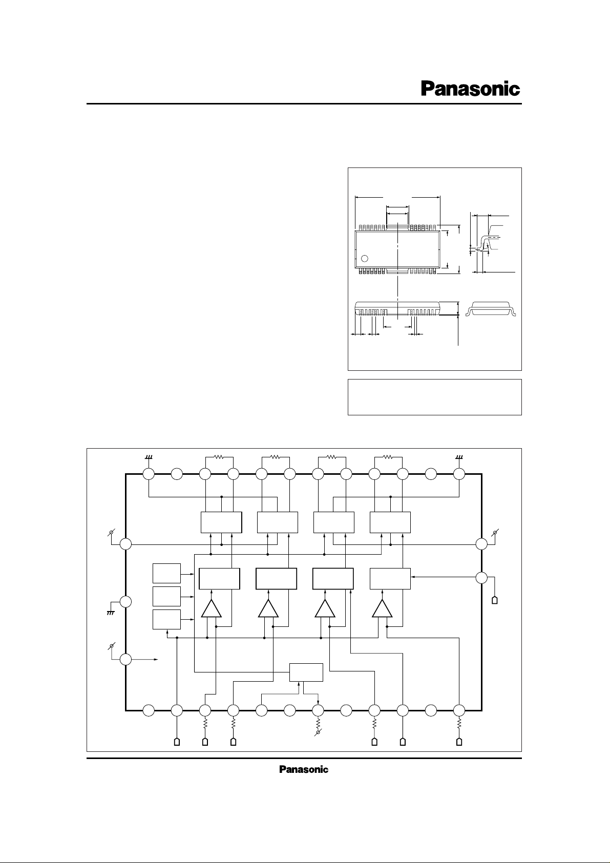
AN8780SB (Under development)
4Ch. Linear Driver IC for CD/CD-ROM
1 14
28 15
18.4±0.20
(5.15)
(4.8)
10.93±0.30
8.3±0.20
(6.4)
(1.2) 0.8
0.35
2.7±0.30
0.65±0.20
0 ~ 10˚
Unit : mm
28 pin, fin attached SOP package (HSOP042-P-0400)
22 21
78
0.10±0.10
+0.10
– 0.05
0.30
+0.10
– 0.05
(1.315)
■ Block Diagram
The AN8780SB is under development, so
these described contents may be revised
without prior notice.
PGND2 NC D4+ D4– D3+ D3– D2+ D2– D1+ D1– NC PGND1
20
21
PV
CC2
FIN
22
SV
CC
232425262728123456
NC V
19 18 17 16 15 14 13 12 11 10
BTL Linear
Driver
Ch.1
Absolute
V–1
Direction
Det.
+–
IN2
Thermal
Protect
V
CC
Monitor
V
REF
Monitor
REF
RESET
BTL Linear
Driver
Ch.2
Absolute
V–1
Direction
Det.
RESET
OUT
V
CC
BTL Linear
Driver
Ch.4
Ch.4 Ch.3 Ch.2 Ch.1
Absolute
V
–1
Direction
Det.
+–
IN4 IN3
BTL Linear
Driver
Ch.3
Absolute
V–1
Direction
Det.
+– +–
RESET
IN
NC NC
PC2
NC
9
8
PV
CC1
PC1
7
IN1
ICs for CD/CD-ROM Player
AN8780SB
Pin No.
Pin Name
1
2
3
4
5
6
7
8
9
10
11
12
13
14
15
Reset output pin
NC
Input pin of motor driver 2
PC 2 (Power Cut) input pin
NC
Input pin for motor driver 1
PC (Power Cut) 1 input pin
V
CC
1 for driver
GND 1 for driver
NC
Reverse rotation output pin of motor driver 1
Normal rotation output pin of motor driver 1
Reverse rotation output pin of motor driver 2
Normal rotation output pin of motor driver 2
Reverse rotation output pin of motor driver 3
■ Pin Description
Pin Name
16
17
18
19
20
21
22
23
24
25
26
27
28
Fin
Normal rotation output pin of motor driver 3
Reverse rotation output pin of motor driver 4
Normal rotation output pin of motor driver 4
GND 2 for driver
V
CC
2 for driver
Supply pin
NC
V
REF
input pin
Input pin of motor driver 4
Input pin of motor driver 3
Reset input pin
NC
GND
Pin No.
V
CC
I
CC
P
D
I
out
T
opr
T
stg
Supply Voltage
Supply Current
Power Dissipation
Note)
Output current
Operating Ambient Temperature
Storage Temperature
V
mA
mW
mA
˚C
˚C
Parameter Symbol Rating Unit
20
3140
500
–30 ~ + 85
–55 ~ +150
Note) For surface mounting on 100 × 80 × 1.6 mm double face glass epoxy board.
■ Absolute Maximum Ratings (Ta=25˚C)
■ Recommended Operating Range (Ta=25˚C)
Parameter Symbol Range
Operating Supply Voltage Range
V
CC
PV
CC
4.5V ~ 14V
 Loading...