

Panasonic AN8737SB Datasheet
ICs for Optical Disk Drive
AN8737SB
3-channel driver IC for optical disk drive
■ Overview
The AN8737SB is a BTL type 3-channel driver
IC, adopting a current feedback system for 2 channels, which makes it optimum for an actuator and a
motor driver of CD-ROM/DVD-ROM. It can also
constitute an optimum system in combination with
the AN8488SB, a spindle plus loading driver IC. A
surface mount-type package of good heat radiation
characteristic is used.
■ Features
• Little phase delay due to a current feedback system
(2 channels for actuator)
• The remaining channel is available for either
traverse or loading motor drive.
• Wide output dynamic range (4 V/I
= 800 mA)
O
• Standby function built in (all channels can be
muted.)
• Thermal shut-down circuit built in
• With thermal flag pin
■ Applications
• CD/CD-ROM player
• DVD/DVD-ROM drive
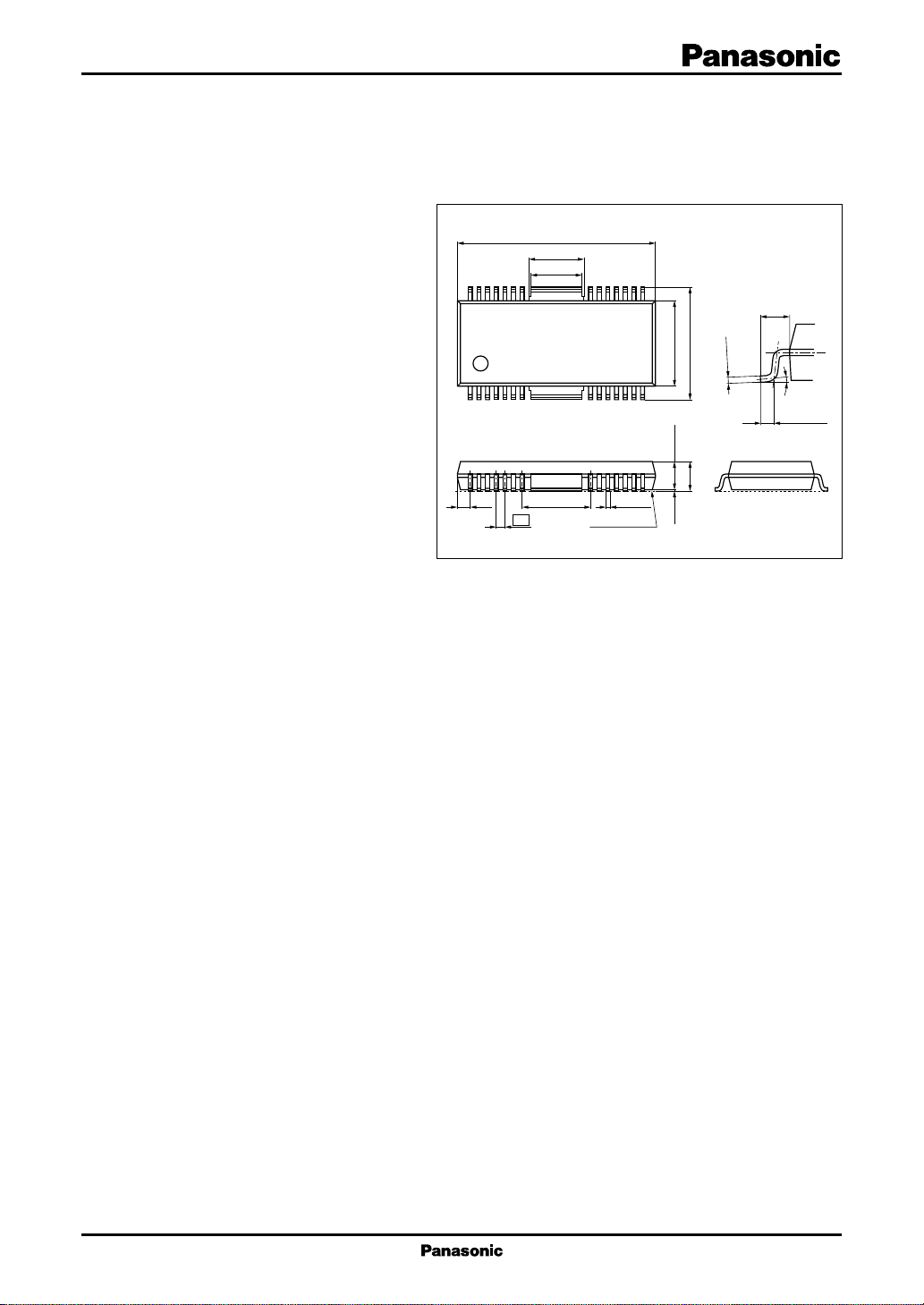
18.4±0.2
(5.15)
28 22 21
17 814
(1.2)
(4.8)
(6.4)
0.8
15
8.3±0.22.7±0.20.1±0.1
+0.10
0.35
–0.05
Seating plane
HSOP042-P-0400
+0.10
10.93±0.30
Unit: mm
(1.315)
–0.05
0.30
0° to 10°
0.65±0.20
1
AN8737SB ICs for Optical Disk Drive
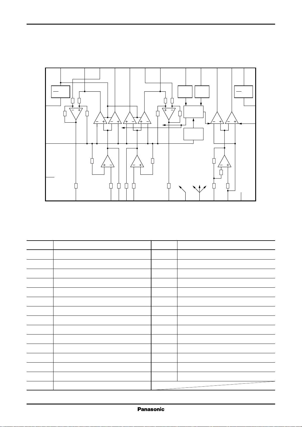
■ Block Diagram
PGND1
V
REF
N.C.
13
26
10
CC1
VO1−
5
VS1
12
VO1+
VO2+
VS2
VO2−
15
28
14
PV
8
1
V
CC
2
9
V
det.
7
CC
CC
SV
TFLG
20
Temp.
det.
16
CC2
VO3−
VO3+
PV
19
21
1
V
CC
2
17
PGND2
Reset
18
PC2
V
REF
reset
6
VRB1
3
IN1
4
OUT1
1
OUT2
2
IN2
27
VFB2
11
PC1
24
SB
23
IN3N
25
IN3P
Fin
SGND
■ Pin Descriptions
Pin No. Description
1 Ch. 2 first stage feedback pin
2 Ch. 2 first stage input pin
3 Ch. 1 first stage input pin
4 Ch. 1 first stage feedback pin
5 Ch. 1 current feedback input pin
6 Ch. 1 current feedback output pin
7 Control side power supply pin
8 Ch. 1 & ch. 2 power side power supply pin
9 Ch. 1 reverse direction output pin
10 N.C.
11 Ch. 1 & Ch. 2 mute pin
12 Ch. 2 forward direction output pin
13 Ch. 1 & ch. 2 power side grounding pin
14 Ch. 2 reverse direction output pin
15 Ch. 2 forward direction output pin
Pin No. Description
16 Ch. 3 reverse direction output pin
17 Ch. 3 power side grounding pin
18 Ch. 3 mute pin
19 Ch. 3 forward direction output pin
20 TDS flag pin
21 Ch. 3 power side power supply pin
22 N.C.
23 Ch. 3 reverse rotation input pin
24 Standby input pin
25 Ch. 3 forward rotation input pin
26 Reference voltage input pin
27 Ch. 2 current feedback output pin
28 Ch. 2 current feedback input pin
Fin Control side grounding pin
2
ICs for Optical Disk Drive AN8737SB
■ Absolute Maximum Ratings
Parameter Symbol Rating Unit
Supply voltage V
Supply voltage range SVCC , PV
2
Supply current
Power dissipation
Operating ambient temperature
Storage temperature
Note)*1: Except for the operating ambient temperature and storage temperature, all ratings are for Ta = 25°C.
2: I
*
PVCC1
3: Use within the range of PD = 542 mW or less at Ta = 85°C, following the allowable power dissipation characteristic curve
*
of "■ Application Notes".
*
3
*
1
*
1
*
be 1 A or less for channel 1 and channel 2, respectively.
I
SVCC
I
PVCC1
I
PVCC2
P
T
T
CC
CC1
D
opr
stg
, PV
CC2
■ Recommended Operating Range
Parameter Symbol Range Unit
Supply voltage SV
PV
CC1
CC
, PV
CC2
14.0 V
− 0.3 to +14.0 V
500 mA
2.0 A
800 mA
542 mW
−30 to +85 °C
−55 to +150 °C
4.5 to 13.5 V
3.5 to 13.5
■ Electrical Characteristics at SVCC = 12 V, PV
VSB = V
PC1
= V
= 3.3 V, V
PC2
IN1
= V
IN2
= V
IN3
= 5 V, PV
CC1
= 5 V, RL = 8 Ω, V
CC2
= 1.65 V, Ta = 25°C
= 1.65 V,
REF
Parameter Symbol Conditions Min Typ Max Unit
= V
= V
, V
Current consumption 1 I
(no signal) VSB = V
Current consumption 2 I
(no signal) VSB = V
Current consumption 1 I
(standby) VSB = V
Current consumption 2 I
(standby) VSB = V
SVOVIN1
PVOVIN1
SVSBVIN1
PVSBVIN1
= V
= V
= V
IN2
PC1
IN2
PC1
IN2
PC1
IN2
PC1
= V
= V
= V
= V
= V
= V
= V
PC2
PC2
PC2
PC2
Driver 1, Driver 2 RL1 , RL2 = 4 Ω, RS1 , RS2 = 0.5 Ω, R
Output offset voltage V
OF1VIN
Gain (+)G1+ VIN = V
= V
REF
±50 mV 9 11 13 dB
REF
REF
REF
REF
REF
IN1
= 2.5 V 25 45 mA
IN3P
= 3.3 V
, V
= 2.5 V 25 45 mA
IN3P
= 3.3 V
, V
= 2.5 V 0.6 1.5 mA
IN3P
= 0 V
, V
= 2.5 V 0.2 1.0 mA
IN3P
= 0 V
, R
= 10 kΩ, RF1 , RF2 = 4.3 kΩ
IN2
−100 0 100 mV
Relative gain (+/−)G1 −1.5 +1.5 dB
Maximum output amplitude (+)V
L1+VIN
= 3.3 V, RL1 , RL2 = 4 Ω 3.65 4.0 V
RS1 , RS2 = 0.5 Ω
Maximum output amplitude (−)V
L1−VIN
= 0 V, RL1 , RL2 = 4 Ω−4.0 −3.65 V
RS1 , RS2 = 0.5 Ω
3
 Loading...