

ICs for Compact Disc/CD-ROM Player
AN8730SB
4-channel driver IC for optical disk
■ Overview
The AN8730SB is a 4-channel driver IC, which can
operate in a low voltage, employing the low power consumption type H-bridge system with a switching regulator. It is especially suited for a portable CD/MD player.
■ Features
• Low power consumption due to PWM control of power
supply
• Wide output D-range independent of the reference volt-
age of the system
• Enable to set input/output gain by an external resistor
• Independent power on/off for 2 channels and simulta-
neous on/off for other 2 channels as well
• Battery voltage detection circuit built-in
• Thermal shut-down circuit (with hysteresis) built-in
■ Applications
• Portable CD/MD
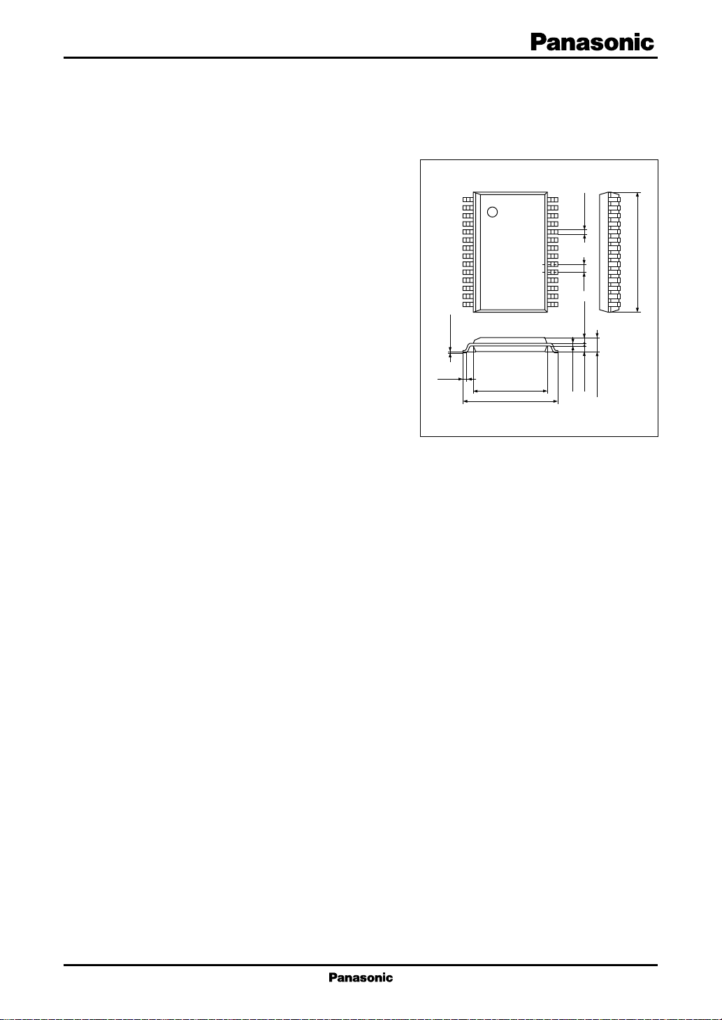
14
0.1±0.1
(0.4)
1
28
15
+0.1
7.2±0.3
9.3±0.3
SSOP028 P-0375A
–0.05
0.2
Unit: mm
0.3±0.1
0.8
0.9±0.1 0.9±0.1
2.05±0.2
11.6±0.3
1
AN8730SB ICs for Compact Disc/CD-ROM Player
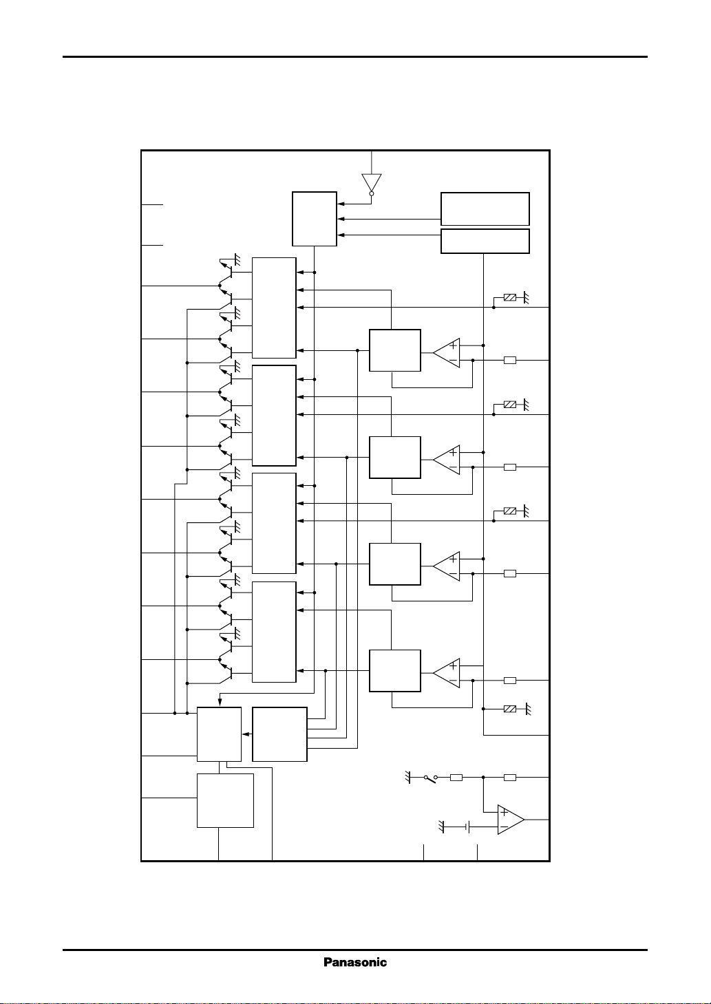
■ Block Diagram
STNBY
12
SGND
PGND
8
21
25
24
23
22
19
20
BTL
BTL
BTL
Power
cut
Absolute
value
Absolute
value
Absolute
value
Thermal
shut-down
V
REF
detection
3
TRVSTOP
4
INTV
6
5
INSP
10
LDON
9
INFO
PC
17
BTL
18
V
TB
CT
Absolute
value
27
C
PWM
26
7
Triangular
Maximum
value
wave
2
28
CLK
PWMG
1
CC
PV
13
CC
SV
11
14
15
16
INTR
V
REF
V
SEN
EMP
2
ICs for Compact Disc/CD-ROM Player AN8730SB
■ Pin Descriptions
Pin No. Symbol Description
1PVCCSupply voltage pin
2 CLK External sync. input pin
3 TRVSTOP Driver on-off control pin
4 INTV Driver input pin
5 INSP Driver input pin
6 PC Driver on-off control pin
7 CT Triangular wave oscillation pin
8 SGND Ground pin
9 INFO Driver input pin
10 LDON Driver on-off control pin
11 INTR Driver input pin
12 STNBY Standby mode input pin
13 SV
14 V
Supply voltage pin
CC
V
REF
input pin
REF
Pin No. Symbol Description
15 V
Empty detection input pin
SEN
16 EMP Empty detection output pin
17 TR− Driver output pin
18 TR+ Driver output pin
19 FO− Driver output pin
20 FO+ Driver output pin
21 PGND Ground pin
22 SP+ Driver output pin
23 SP− Driver output pin
24 TV+ Driver output pin
25 TV− Driver output pin
26 TB PWM circuit output pin
27 V
Drive supply voltage pin
C
28 PWMG PWM loop gain adjustment pin
■ Absolute Maximum Ratings
Parameter Symbol Rating Unit
Supply voltage PV
Supply voltage range PV
Supply current I
Supply current 1 I
Supply current 2 I
Drive output current I
2
Power dissipation
Max. application voltage to V
Operating ambient temperature
Storage temperature
Note) 1. Do not apply external currents or voltages to any pins not specifically mentioned.
For circuit currents, '+' denotes current flowing into the IC, and '−' denotes current flowing out of the IC.
1: Except for the operating ambient temperature and storage temperature, all ratings are for Ta = 25°C.
2. *
2: Ta = 75°C. For the independent IC without a heat sink. Refer to "■ Application Note" at mounting on PCB.
*
*
pin V
SEN
1
*
1
*
SV
V
SV
SVCC
PVCC
P
10max
T
T
CC
CC
C
CC
CC
CC
O
D
opr
stg
15 V
6
9
− 0.3 to +15.0 V
− 0.3 to +6.0
mA
50 mA
100 mA
500 mA
345 mW
15.0 V
−25 to +75 °C
−55 to +125 °C
■ Recommended Operating Range
Parameter Symbol Range Unit
Supply voltage PV
SV
CC
CC
2.7 to 14.0 V
2.7 to 5.5
3
 Loading...