

■ Overview
The AN8612NSR is a terminator IC complying with the standard interface standards [SCSI-I/II] for personal computer,
work station and various information equipment. Fixed resistor
and regulator which are separately provided in conventional
ICs are incorporated in single chip for the AN8612NSR. The
stand-by function is also built in the AN8612NSR. Moreover,
this IC can easily satisfy the maximum terminal capacitance of
25 pF of the SCSI-II standard, because of its small output terminal capacitance. It can support the 10 M byte/s of SCSI-II
and 20 M bytes/s of Fast-20.
■ Features
•
Active termination of 18 signal lines
•
Low consumption power owing to stand-by function built-in
(100µA in stand-by condition)
•
Small output terminal capacitance : 4.5 pF, typ.
•
High accuracy regulator : 2.85V±60mV
■ Application
SCSI interface board of PC
SCSI equipment such as CD-ROM, MO, PD and MD printer
AN8612NSR
SCSI Active Terminator IC
8.4±0.3
11.73±0.3
0.5
0.1±0.1
(0075)
3.15±0.2
1.45
(7.8)
(9.2)
1.27 0.4±0.25
(6.0)
(4.6)
16.0±0.3
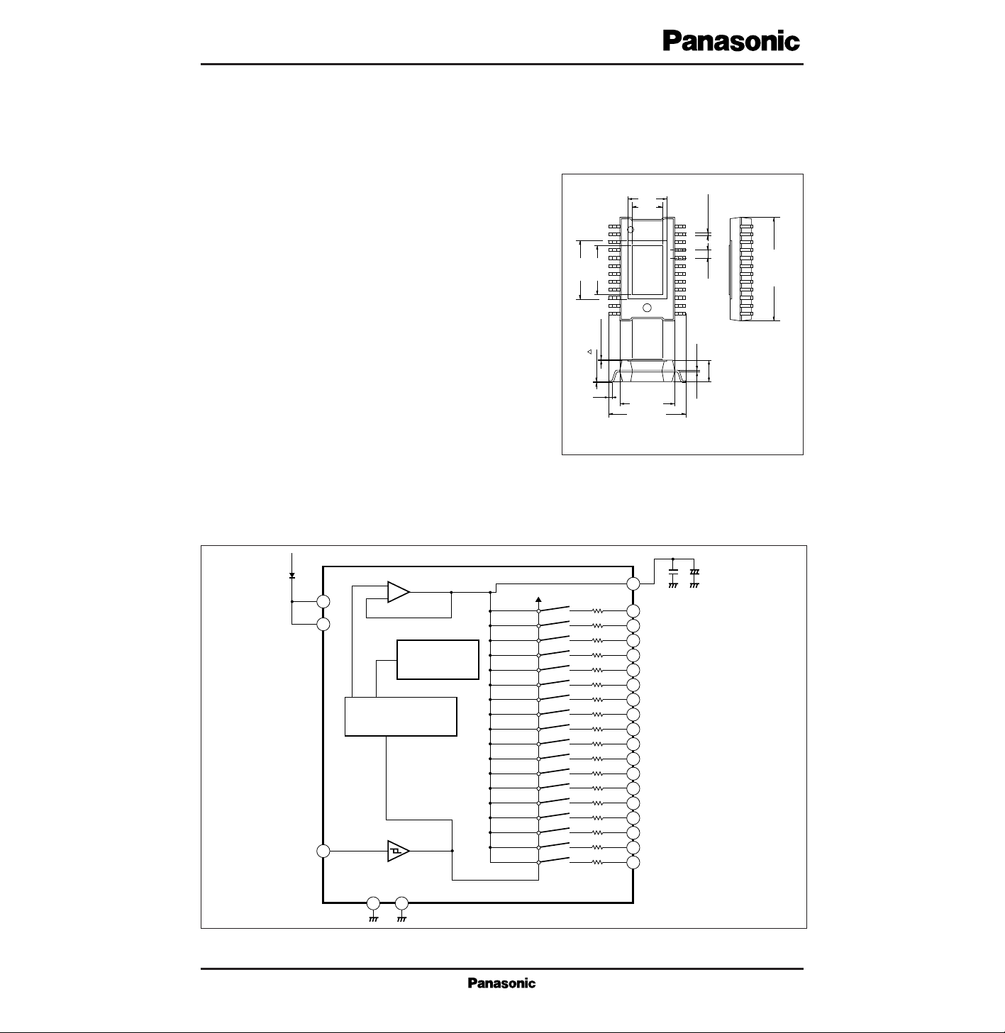
Unit : mm
1.45
1
2
4
5
6
7
8
9
11
12
3
10
24
23
22
21
20
19
18
17
16
15
14
13
Number in ( ) is a reference value.
24-pin SOP Package (HSOP024-P-0450)
(0.2)
■ Block Diagram
0.1µF
+
1µF
V
CC
12
13
STANDBY
24
+
–
Band Gap
Reference
6 19
Thermal
Shut Down
1
18
SG LINE 1
17
SG LINE 2
16
SG LINE 3
15
SG LINE 4
14
SG LINE 5
11
SG LINE 6
10
SG LINE 7
9
SG LINE 8
8
SG LINE 9
7
SG LINE 10
5
SG LINE 11
4
SG LINE 12
3
SG LINE 13
2
SG LINE 14
23
SG LINE 15
22
SG LINE 16
21
SG LINE 17
20
SG LINE 18
V
CC
I
CC
P
D
T
opr
T
stg
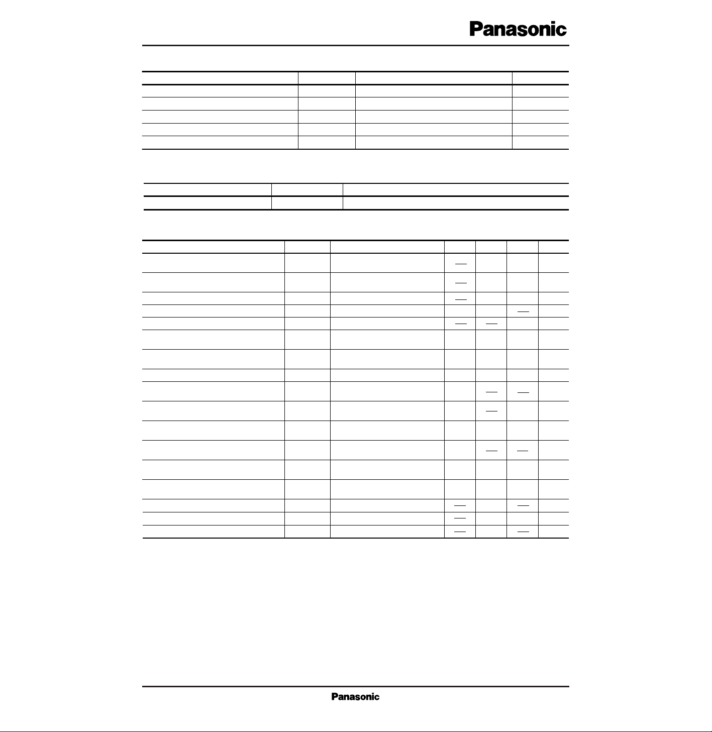
Supply voltage
Supply current
Power dissipation
Note)
Operating ambient temperature
Storage temperature
V
mA
mW
˚C
˚C
Parameter Symbol Rating Unit
– 0.3 to + 7.0
500
2250
–20 to + 60
–55 to + 150
■ Recommended Operation Range (Ta=25˚C)
V
CC
Operating supply voltage
Parameter Symbol Range
4.0V to 5.5V
Parameter Symbol Condition min typ max Unit
■ Electrical Characteristics (VCC=5.0V, Ta=25±2˚C)
Supply current 1 44
I
CC1
54 mA
STANDBY= “L”
All SGLINE=open
STANDBY terminal “L” input current
Supply current 2 458
I
CC2
530 mA
STANDBY= “L”
All SGLINE=0.2V
V
CC
=5.5V, VI=0V
Supply current 3 100I
CC3
I
STBYL
200
1
µASTANDBY=open
–150 –50
1.3 1.5
µA
VSG=0.2VI
SG
19.8 23.0 26.2 mA
STANDBY terminal “L” input current VCC=5.5V, VI=5.5V
ISG=5mA to 15mA
I
STBYH
µA
1.7
STANDBY terminal positive direction
Threshold voltage
V
TH+
V
1.1 1.3 1.5
STANDBY terminal negative direction
Threshold voltage
V
TH–
V
Maximum output current SGLINE1-18
VCC=5.5V
STANDBY=open, V
SG
=0V
I
LK1
–1 µA
Output leak current 1
SGLINE1 to 18
VCC=5.5V
STANDBY=open, V
SG
=2.85V
I
LK2
–1 1 µA
Output leak current 2
SGLINE1 to 18
VCC=4.0 to 5.5V
All SGLINE=open
V
SGH
2.78 2.85 2.92 V
“H” level output voltage
SGLINE1 to 18
R
SG
107 115 123 Ω
Termination resistance value
SGLINE1 to 18
VCC=4.0 to 5.5V
All SGLINE=open
V
REG1
2.79 2.85 2.91 V
REG · output voltage
VCC=3.2V
All SGLINE=open
V
REG2
2.00 V
REG · output voltage
STANDBY terminal hysteresis width
V
HYS
mV
Output terminal capacitance
C
SG
8 pF
Thermal shut-down temperature T
TSD
˚C
(4.5)
(200)
(170)
Note) Number in ( ) is a design reference value but not guaranteed one.
 Loading...