

Panasonic AN8000MS Technical data
f
查询AN8000MS供应商
Voltage Regulators
AN8000MS
Ripple filter IC for cellular phones
■ Overview
The AN8000MS is a ripple filter IC that rejects the
ripple component superimposed on the regulator output.
Use for the VCO bias of cellular phones improves C/N
and S/N and makes the high-quality telephone communication possible. Furthermore, by decreasing the difference between I/O voltages, drop in the power supply voltage of VCO is reduced.
■ Features
• The I/O drop voltage is reduced to 0.3 V (A PNP transistor is used for the pass transistor)
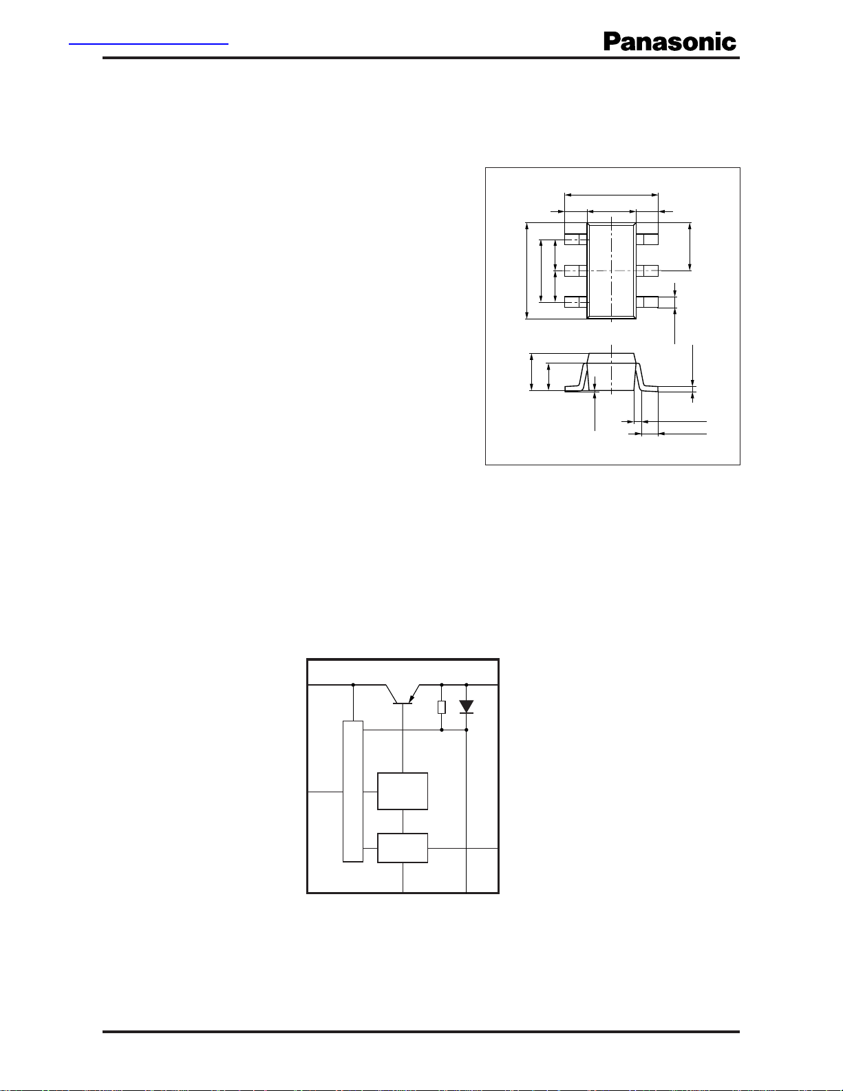
• The mounting area is reduced by adopting the mini-type
6-pin package
■ Applications
• Cellular phones and others
+0.20
2.90
+0.2
–0.05
1.10
1.90±0.20
–0.1
(0.80)
(0.95) (0.95)
6
5
4
+0.20
2.80
–0.30
+0.25
1.50
–0.05
0 to 0.10
MINI-6D
(0.65)(0.65)
Unit: mm
1
2
3
+0.10
–0.05
0.30
0.10 to 0.30
0.40±0.20
(1.45)
–0.06
+0.10
0.16
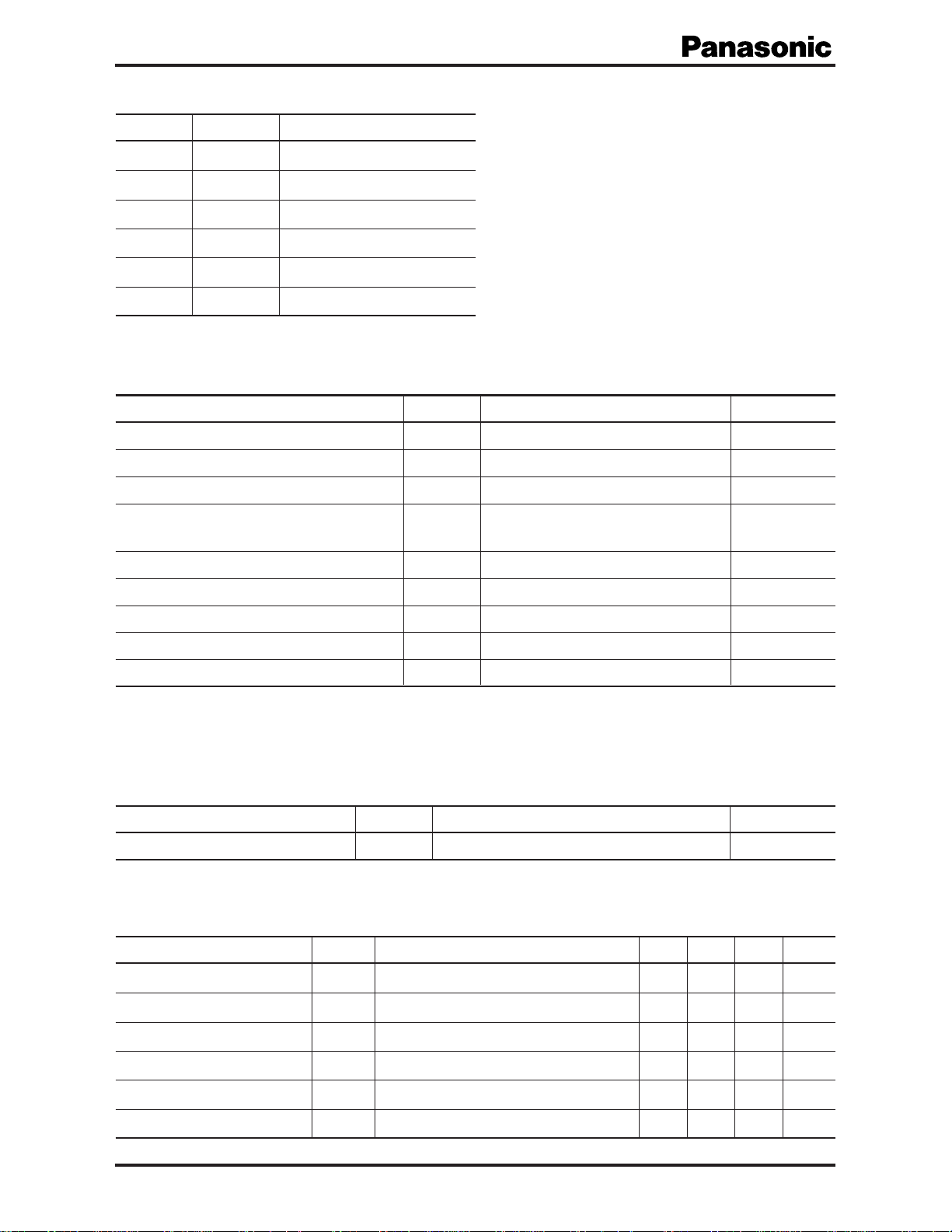
■ Block Diagram
VOUT
C2
4
2
Constant
1
VIN
current
Voltage control
Switch
6
On/Of
35
C1GND
Publication date: August 2001 SDH00013AEB
1
AN8000MS
■ Pin Descriptions
Pin No. Symbol Description
1 VIN Input pin
2 C2 Capacitor connection pin 2
3 C1 Capacitor connection pin 1
4 VOUT Output pin
5 GND Ground pin
6 On/Off Control pin
■ Absolute Maximum Ratings
Parameter Symbol Rating Unit
Supply voltage V
Supply current I
Output current I
Allowable application voltage for V
ON/OFF
IN
IN
O
7.0 V
20 mA
−15 mA
V
IN
on/off pin
Allowable maximum capacitance for C1 pin C
Allowable maximum capacitance for C2 pin C
2
Power dissipation
Operating ambient temperature
Storage temperature
Note)*1: Except for the operating ambient temperature and storage temperature, all ratings are for Ta = 25°C.
2: The power dissipation shown is the value for Ta = 75°C.
*
*
1
*
1
*
1
2
P
D
T
opr
T
stg
100 µF
10 µF
60 mW
−25 to +75 °C
−40 to +125 °C
■ Recommended Operating Range
Parameter Symbol Range Unit
Supply voltage V
CC
2.5 to 6.5 V
V
■ Electrical Characteristics at Ta = 25°C
Parameter Symbol Conditions Min Typ Max Unit
Output voltage 1 V
Output voltage 2 V
Output voltage 3 V
Output voltage 4 V
Output voltage 5 V
Output voltage 6 V
2
O1
O2
O3
O4
O5
O6
VIN = 2.5 V, I
VIN = 2.5 V, I
VIN = 3.0 V, I
VIN = 3.0 V, I
VIN = 7.0 V, I
VIN = 7.0 V, I
=−1 µA 2.10 2.27 V
OUT
=−15 mA 1.95 2.14 V
OUT
=−1 µA 2.60 2.79 V
OUT
=−15 mA 2.60 2.66 V
OUT
=−1 µA 6.70 6.87 V
OUT
=−15 mA 6.60 6.74 V
OUT
SDH00013AEB
 Loading...