

Panasonic AN77L06M, AN77L06, AN77L05M, AN77L05, AN77L04M Datasheet
...
■ Overview
The AN77L00/AN77L00M series is a stabilized constant
voltage power supply with a low input/output voltage(0.3V
max.). It is suitable for the low-voltage equipment using
batteries, and consumer/industrial equipment with great
fluctuation of the supply voltage.
A wide range of output voltage is available from 3V
through 10V.
■ Features
• Minimum input/output voltage difference : 0.3V(max.)
• Built-in overcurrent limiting circuit
• Built-in rush current preventive circuit at saturation volt-
age rise time
• Built-in overheat protective circuit
• Built-in input short-circuit protective circuit
1
Voltage Regulators
AN77L00/AN77L00M Series
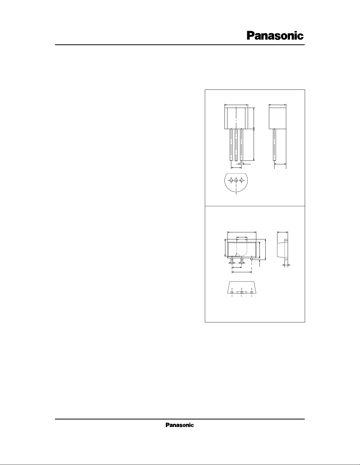
3-pin Low Power Loss Voltage Regulato r(100mA Type)
AN77L00 Series
Unit : mm
5.0
±0.2
2.3±0.2
5.1±0.213.5±0.5
0.45
+0.2
– 0.1
2.54
4.0±0.2
213
3-pin SIL Plastic Package (TO-92) (SSIP003-P-0000)
AN77L00M Series Unit : mm
3-pin SIL Mini Power Type Plastic Package (TO-220F) (SSIP003-P-0000D)
4.6max.
1.6max.
0.44max.
0.48max.
1.8max.
1.5
3.0
2.6max.
4.25max.
0.8min.
2.6
0.58max.
4.5
123

2
Voltage Regulators
AN77L00/AN77L00M Series
3 12
–
+
IN
(1)
GND
(3)
OUT
(2)
The pin numbers in are for the AN77L00M series.
The pin numbers in ( ) are for the AN77L00 series.
Error Amp.
Starter
Voltage
Reference
Input Short-Circuit
Protection
Over Current
Protection
Over Current
Protection
Rush Current
Protection
Thermal
Protection
■ Block Diagram
V
IN
I
IN
P
D
T
opr
T
stg
Supply voltage
Supply current
Power dissipation
Note1)
Operating ambient temperature
Storage temperature
V
mA
mW
˚C
˚C
Parameter Symbol Rating Unit
■ Absolute Maximum Ratings (Ta=25˚C)
30
200
650
–30 to + 85
–55 to + 150
Note 1)
Part No. Output voltage (VO) Operating supply voltage range (VI)
■ Recommended Operating Range (Ta= 25˚C)
AN77L03/M
AN77L035/M
AN77L04/M
AN77L045/M
AN77L05/M
AN77L06/M
AN77L07/M
AN77L08/M
AN77L09/M
AN77L10/M
AN77L12/M
3
3.5
4
4.5
5
6
7
8
9
10
12
VO + 0.3 to 13.62
VO + 0.41 to 14.14
VO + 0.3 to 14.66
VO + 0.43 to 15.18
VO + 0.3 to 15.7
VO + 0.46 to 16.74
VO + 0.48 to 17.78
VO + 0.51 to 18.82
VO + 0.53 to 19.86
VO + 0.55 to 20.9
VO + 0.6 to 22.98
V
V
V
V
V
V
V
V
V
V
V
Unit
3
Voltage Regulators
AN77L00/AN77L00M Series
Output voltage
Input stability
Load stability
Bias current under no load
Bias current fluctuation under load
Bias current before regulation start
Ripple rejection ratio
Min. input/output voltage difference (1)
Min. input/output voltage difference (2)
Output noise voltage
Output voltage temperature coefficient
V
O
REG
IN
REG
L
I
bias
∆I
bias
I
rush
RR
V
DIF (min) 1
V
DIF (min) 2
V
no
∆VO/Ta
Tj=25˚C
V
I
=3.62 to 13.62V, Tj=25˚C
I
O
=0 to 100mA, Tj=25˚C
I
O
=0mA, Tj=25˚C
I
O
=0 to 100mA, Tj=25˚C
V
I
=2.7V, IO=0mA, Tj=25˚C
V
I
=3.62 to 5.62V, f=120Hz
V
I
=2.7V, IO=50mA, Tj=25˚C
V
I
=2.7V, IO=100mA, Tj=25˚C
f=10Hz to 100kHz
T
j
= –30 to+125˚C
2.88
60
3
2
8
0.9
3
1.5
70
0.12
0.22
70
0.2
3.12
60
60
1.5
5
5
0.25
0.3
V
mV
mV
mA
mA
mA
dB
V
V
µV
mV/˚C
Parameter Symbol Condition min typ max Unit
■ Electrical Characteristics (Ta=25˚C)
• AN77L03/M (3V, 100mA Type)
Note 1) Under Tj=25˚C, each test duration can be set short (within 10ms) and the characteristic drift with temperature rise at
joints of the chip may be ignored.
Note 2) VI=4V, IO=50mA, CO=10µF unless otherwise specified.
Output voltage
Input stability
Load stability
Bias current under no load
Bias current fluctuation under load
Bias current before regulation start
Ripple rejection ratio
Min. input/output voltage difference (1)
Min. input/output voltage difference (2)
Output noise voltage
Output voltage temperature coefficient
T
j
=25˚C
V
I
= 4.14 to 14.14V, Tj=25˚C
I
O
= 0 to 100mA, Tj= 25˚C
I
O
= 0mA, Tj= 25˚C
I
O
= 0 to 100mA, Tj= 25˚C
V
I
= 3.15V, IO= 0mA, Tj=25˚C
V
I
= 4.14 to 6.14V, f=120Hz
V
I
= 3.15V, IO= 50mA, Tj= 25˚C
V
I
= 3.15V, IO=100mA, Tj= 25˚C
f=10Hz to 100kHz
T
j
= –30 to+125˚C
3.36
59
3.5
3
9
0.9
3
1.5
69
0.12
0.22
75
0.23
3.64
60
60
1.5
5
5
0.25
0.41
Parameter Symbol Condition min typ max Unit
•
AN77L035/M (3.5V, 100mA Type)
Note 1) Under Tj=25˚C, each test duration can be set short (within 10ms) and the characteristic drift with temperature rise at
joints of the chip may be ignored.
Note 2) VI=4.5V, IO=50mA, CO=10µF unless otherwise specified.
V
O
REG
IN
REG
L
I
bias
∆I
bias
I
rush
RR
V
DIF (min) 1
V
DIF (min) 2
V
no
∆VO/Ta
V
mV
mV
mA
mA
mA
dB
V
V
µV
mV/˚C
Output voltage
Input stability
Load stability
Bias current under no load
Bias current fluctuation under load
Bias current before regulation start
Ripple rejection ratio
Min. input/output voltage difference (1)
Min. input/output voltage difference (2)
Output noise voltage
Output voltage temperature coefficient
T
j
=25˚C
V
I
= 4.66 to 14.66V, Tj= 25˚C
I
O
= 0 to 100mA, Tj= 25˚C
I
O
= 0mA, Tj= 25˚C
I
O
= 0 to 100mA, Tj=25˚C
V
I
=3.6V, IO= 0mA, Tj= 25˚C
V
I
= 4.66 to 6.66V, f=120Hz
V
I
=3.6V, IO=50mA, Tj= 25˚C
V
I
=3.6V, IO=100mA, Tj= 25˚C
f=10Hz to 100kHz
T
j
= –30 to+125˚C
3.84
59
4
3
9
0.9
3
1.5
69
0.12
0.23
80
0.26
4.16
60
60
1.5
5
5
0.25
0.3
Parameter Symbol Condition min typ max Unit
•
AN77L04/M (4V, 100mA Type)
Note 1) Under Tj=25˚C, each test duration can be set short (within 10ms) and the characteristic drift with temperature rise at
joints of the chip may be ignored.
Note 2) VI=5V, IO=50mA, CO=10µF unless otherwise specified.
V
O
REG
IN
REG
L
I
bias
∆I
bias
I
rush
RR
V
DIF (min) 1
V
DIF (min) 2
V
no
∆VO/Ta
V
mV
mV
mA
mA
mA
dB
V
V
µV
mV/˚C
 Loading...