

Voltage Regulators
2.54 2.54
0.8
(2.0) (2.5)
10.5±0.3
+0.15
–0.05
1.4
+0.15
–0.05
0.45
+0.2
–0.0
(4.5) 8.7±0.2
15.4±0.2
2.9±0.1
12.5±0.2
17.0±0.2
26.1±0.2
29.0±0.3
(13.6)
(10.35) 4.5±0.2
10.0±0.3 1.4±0.1
φ3.7±0.1
6.50±0.10
5.30±0.10
4.35±0.20
4.60±0.10
2.30
0.75±0.10
123
0.80max.
1.00±0.30
1.80±0.30
1.00±0.20
0.10±0.05
0.55±0.15
3.00±0.20
2.50±0.20
5.50±0.20
0.20max.
9.80±0.10
7.30±0.10
2.30±0.10
AN7700, AN7700F, AN7700SP Series
Low-dropout three-pin voltage regulator 1.2-A type
■ Overview
The AN7700, AN7700F, and AN7700SP series are
stabilized constant-voltage power supplies with small difference between I/O voltages (0.5 V typ.). They are suitable for low-voltage, battery-driven equipment, and home
appliances and industrial equipment with great fluctuation of the supply voltage.
The output voltage ranges:
For AN7700, AN7700F
3 V, 4 V, 5 V, 6 V, 7 V, 8 V, 9 V, 10 V, 12 V, 15 V,
18 V, 20 V, and 24 V
For AN7700SP
3.3 V, 3.5 V, 5 V, 6 V, 7 V, 8 V, 9 V, 10 V, 12 V,
and 15 V
■ Features
• Minimum I/O voltage difference: 0.5 V (typ.)
• On-chip overcurrent limiter
• On-chip thermal protection circuit
• On-chip inrush current protection circuit at the time of
input voltage start-up
• On-chip input short-circuit protection circuit
(When the input pin is short-circuited to the ground, the
circuit between pins 1 and 3 is shut down to prevent
current flow.)
■ Applications
• Power supply equipment
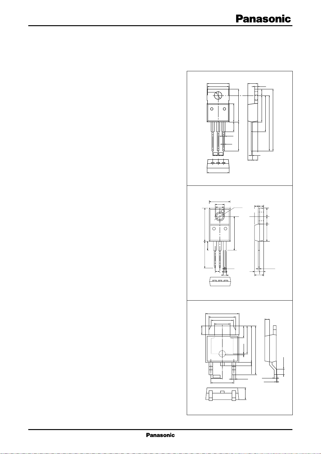
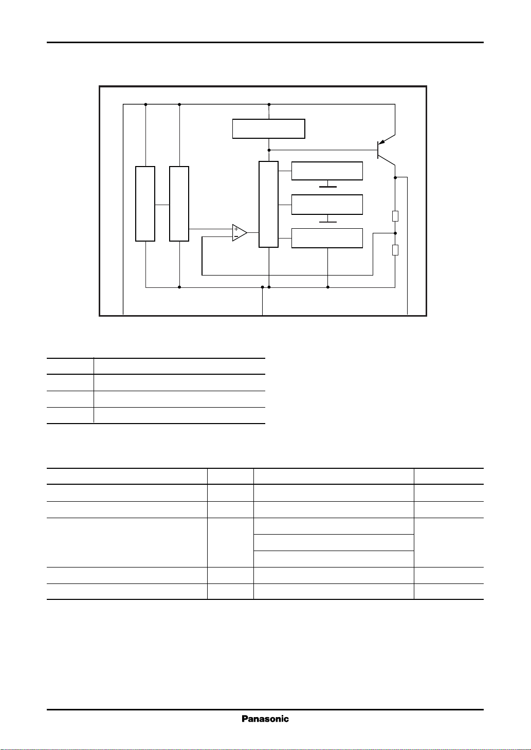
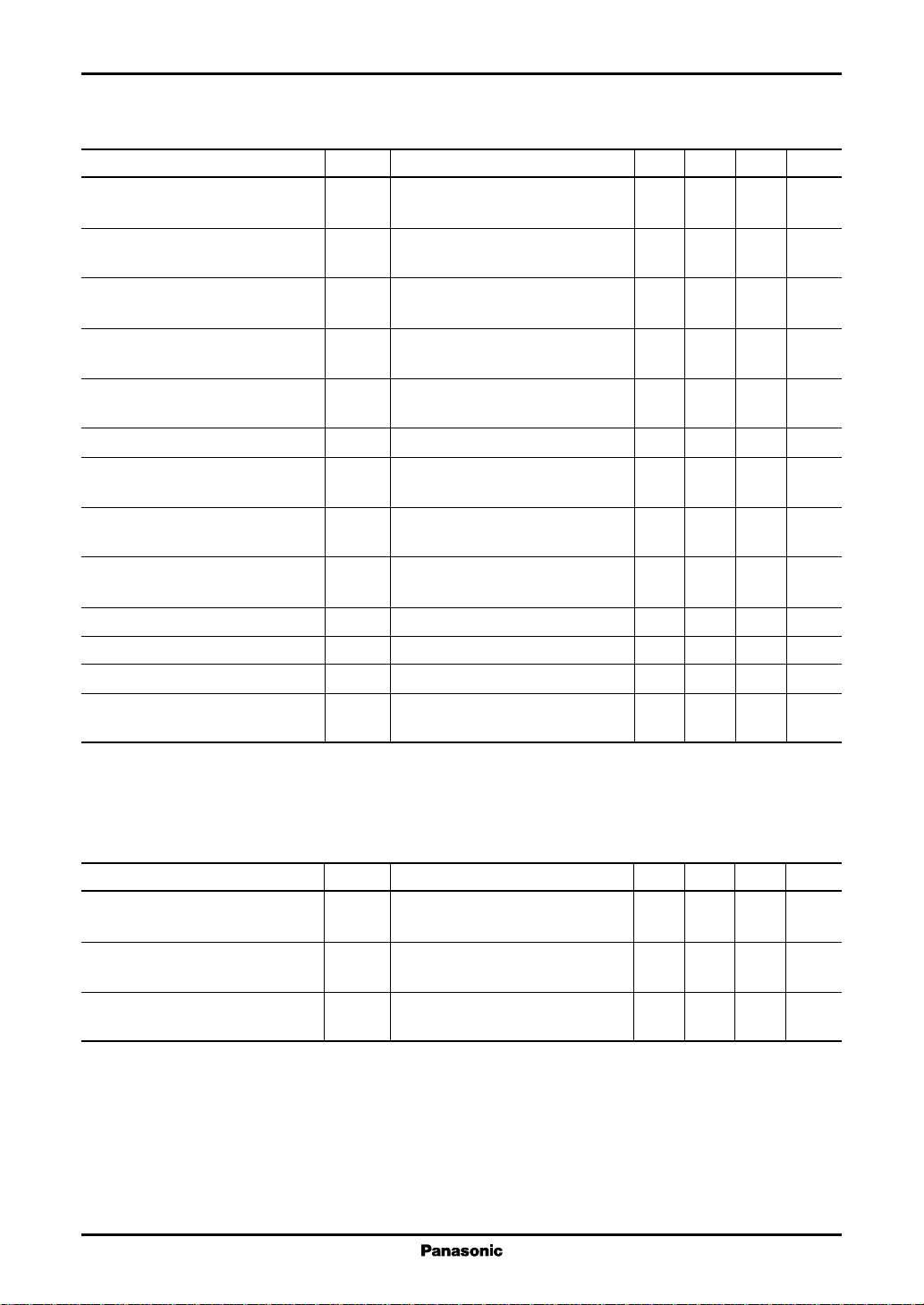
AN7700 series Unit: mm
TO-220 Package (HSIP003-P-0000)
AN7700F series Unit: mm
10.5±0.3
(4.3)
4.5±0.25
13.6±0.25 16.7±0.3
φ5.3
2.54
123
(0.4)
0.8±0.2
1.4±0.2
3.1±0.1
17.0±0.25
(1.73)
2.0
±0.25
2.77±0.3
4.5±0.3
+0.1
0.4
–0.05
2.5±0.25
4.2±0.25
±0.25
8.7±0.3 3.8
TO-220F Package (HSIP003-P-0000A)
AN7700SP series Unit: mm
U-type Package
1
AN7700, AN7700F, AN7700SP Series Voltage Regulators
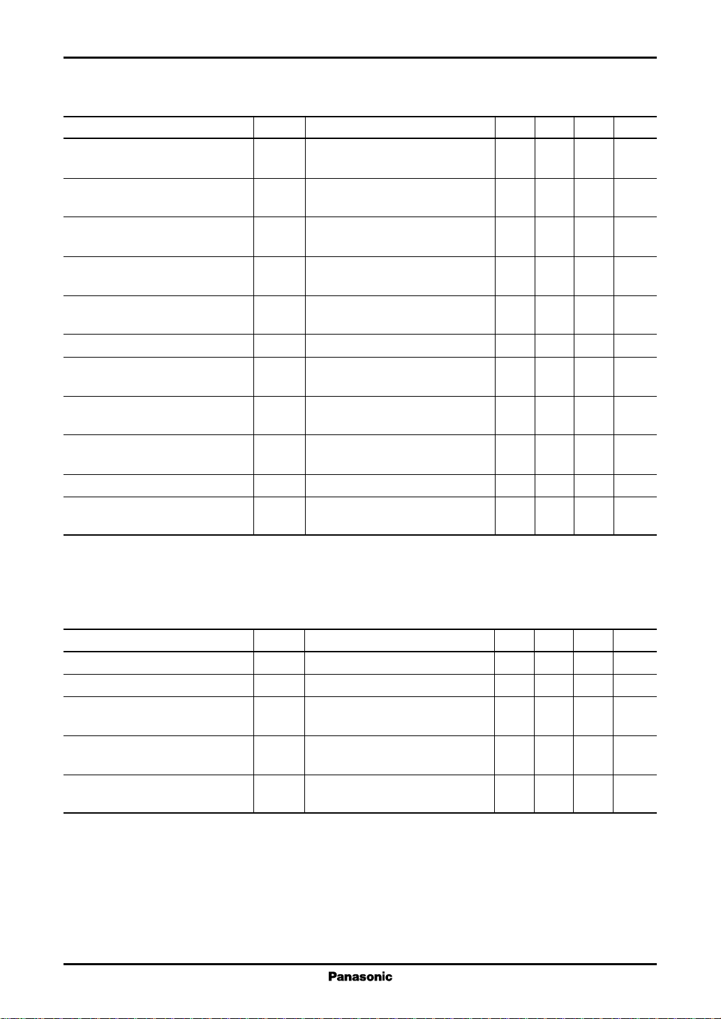
■ Block Diagram
Starter
1
■ Pin Descriptions
Pin No. Description
1 Input pin (In)
2 Ground pin (COM)
3 Output pin (Out)
V
REF
Voltage reference
Error amplifier
Input short-circuit
protection
Output driver
2
Output stage
Overcurrent
limiter
Inrush current
protection
R1
Thermal
protection
R2
3
■ Absolute Maximum Ratings at Ta = 25°C
Parameter Symbol Rating Unit
2
Supply voltage
Supply current
Power dissipation
Operating ambient temperature
Storage temperature
Note)*1: Expect for the operating ambient temperature, and storage temperature, all ratings are for Ta = 25°C.
2: At the application of VIN = 30 V, the overvoltage protection may be operated by the ASO protection circuit, leading to the
*
output shut down.
3: The current value does not exceed this criterion because of the on-chip current limiter.
*
4: The internal circuit shuts off the output when Tj ≥ 150°C (designed value). The relationship between the IC power
*
dissipation and ambient temperature shall conform to the derating curve (■ Characteristic curve chart PD Ta).
2
*
3
*
4
*
AN7700 series P
V
IN
I
IN
D
AN7700F series 10.25
AN7700SP series 5.0
1
*
1
*
T
opr
T
stg
30 V
2.4 A
15 W
−30 to +85 °C
−55 to +150 °C

Voltage Regulators AN7700, AN7700F, AN7700SP Series
■ Recommended Operating Conditions at I
Part No. Output voltage Operating supply voltage range (VIN) Unit
AN7703/F 3 4 to 14 V
AN77033SP 3.3 4.3 to 14 V
AN77035SP 3.5 4.5 to 14 V
AN7704/F 4 5 to 15 V
AN7705/F/SP 5 6 to 16 V
AN7706/F/SP 6 7 to 17 V
AN7707/F/SP 7 8 to 18 V
AN7708/F/SP 8 9 to 19 V
AN7709/F/SP 9 10 to 20 V
AN7710/F/SP 10 11 to 21 V
AN7712/F/SP 12 13 to 23 V
AN7715/F/SP 15 16.5 to 26.5 V
AN7718/F 18 19.5 to 29.5 V
AN7720/F 20 21.5 to 29.5 V
AN7724/F 24 25.5 to 29.5 V
= 500 mA, Ta = 25°C
OUT
3
AN7700, AN7700F, AN7700SP Series Voltage Regulators
■ Electrical Characteristics at Ta = 25°C
• AN7703/F (3-V type)
Parameter Symbol Conditions Min Typ Max Unit
Output voltage V
OUTVIN
= 4 V, I
Tj = 25°C
Line regulation REG
INVIN
= 4 V to 14 V, I
Tj = 25°C
Load regulation REG
LOAVIN
= 4 V, I
Tj = 25°C
Input dependency of bias current ∆I
Bias(IN)VIN
= 4 V to 14 V, I
Tj = 25°C
Load dependency of bias current ∆I
Bias(LOA)VIN
= 4 V, I
Tj = 25°C
Bias current at no load I
Bias current I
Bias
rush
VIN = 4 V, I
VIN = 2.7 V, I
before the regulation starts
Minimum I/O voltage difference 1 V
DIF(min)1VIN
= 3.5 V, I
Tj = 25°C
Minimum I/O voltage difference 2 V
DIF(min)2VIN
= 3.5 V, I
Tj = 25°C
Peak output current 1
Peak output current 2
Peak output current 3
Ripple rejection ratio RR V
*
*
*
I
O(Peak)1VIN
I
O(Peak)2VIN
I
O(Peak)3VIN
= 4 V, Tj = 25°C 1.2 1.8 2.4 A
= 13 V, Tj = 25°C 1.0 1.5 2.0 A
= 18 V, Tj = 25°C 0.5 1.0 1.5 A
= 4 V to 6 V, I
IN
f = 120 Hz
Note)*: This current exceeds P
it shall conform to the derating curve ( ■ Characteristic curve chart PD Ta ).
because it is a parameter during abnormal (overcurrent) operation. However, normally,
D(max)
= 500 mA, 2.91 3.00 3.09 V
OUT
= 500 mA, 330mV
OUT
= 0 mA to 1 200 mA, 15 60 mV
OUT
= 500 mA, 110mA
OUT
= 0 mA to 1 200 mA, 10 50 mA
OUT
= 0 mA 2.6 5.0 mA
OUT
= 0 mA 35mA
OUT
= 500 mA, 0.4 0.6 V
OUT
= 1 200 mA, 0.5 1.0 V
OUT
= 100 mA, 54 74 dB
OUT
• Design reference data
Note) The characteristics listed below are theoretical values based on the IC design and are not guaranteed.
Parameter Symbol Conditions Min Typ Max Unit
Output short-circuit current I
O(Short)VIN
= 30 V, Tj = 25°C 10 mA
The load is shorted.
Thermal protection operating T
j(TH)VIN
= 4 V 150 °C
temperature
Output voltage temperature a V
= 5 V, Tj = 25°C to 125°C −40 ppm/°C
IN
coefficient
4
Voltage Regulators AN7700, AN7700F, AN7700SP Series
■ Electrical Characteristics at Ta = 25°C (continued)
• AN77033SP (3.3-V type)
Parameter Symbol Conditions Min Typ Max Unit
Output voltage V
OUTVIN
= 4.3 V, I
Tj = 25°C
Line regulation REG
Load regulation REG
Input dependency of bias current ∆I
Load depndency of bias current ∆I
Bias current at no load I
Bias current I
Bias(IN)VIN
Bias(LOA)VIN
Bias
rush
LOAVIN
= 4.3 V to 14.3 V, 335mV
INVIN
I
= 500 mA, Tj = 25°C
OUT
= 4.3 V, 15 70 mV
I
= 0 mA to 1 200 mA, Tj = 25°C
OUT
= 4.3 V to 14.3 V, 110mA
I
= 500 mA, Tj = 25°C
OUT
= 4.3 V, 10 50 mA
I
= 0 mA to 1 200 mA, Tj = 25°C
OUT
VIN = 4.3 V, I
VIN = 3.0 V, I
before the regulation starts
Minimum I/O voltage difference 1 V
DIF(min)1VIN
= 3.7 V, I
Tj = 25°C
Minimum I/O voltage difference 2 V
DIF(min)2VIN
= 3.7 V, I
Tj = 25°C
Peak output current 1
Ripple rejection ratio RR V
Note)*: This current exceeds P
it shall conform to the derating curve ( ■ Characteristic curve chart PD Ta ).
*
D(max)
I
O(Peak)1VIN
because it is a parameter during abnormal (overcurrent) operation. However, normally,
= 4.3 V, Tj = 25 °C 1.2 1.8 2.4 A
= 4.3 V to 8.0 V, 53 74 dB
IN
I
= 100 mA, f = 120 Hz
OUT
= 500 mA, 3.20 3.30 3.40 V
OUT
= 0 mA 2.6 5.0 mA
OUT
= 0 mA 35mA
OUT
= 500 mA, 0.4 0.6 V
OUT
= 1 200 mA, 0.5 1.0 V
OUT
• Design reference data
Note) The characteristics listed below are theoretical values based on the IC design and are not guaranteed.
Parameter Symbol Conditions Min Typ Max Unit
Peak output current 2
Peak output current 3
Output short-circuit current I
*
*
I
O(Peak)2VIN
I
O(Peak)3VIN
O(Short)VIN
= 13.3 V, Tj = 25°C 1.5 A
= 18.3 V, Tj = 25°C 1.0 A
= 30 V, Tj = 25°C 10 mA
The load is shorted.
Thermal protection operating T
j(TH)VIN
= 4.3 V 150 °C
temperature
Output voltage temperature a V
= 4.3 V, Tj = 25°C to 125°C −40 ppm/°C
IN
coefficient
Note)*: This current exceeds P
it shall conform to the derating curve ( ■ Characteristic curve chart PD Ta ).
because it is a parameter during abnormal (overcurrent) operation. However, normally,
D(max)
5
AN7700, AN7700F, AN7700SP Series Voltage Regulators
■ Electrical Characteristics at Ta = 25°C (continued)
• AN77035SP (3.5-V type)
Parameter Symbol Conditions Min Typ Max Unit
Output voltage V
OUTVIN
= 4.5 V, I
Tj = 25°C
Line regulation REG
Load regulation REG
Input dependency of bias current ∆I
Load dependency of bias current ∆I
Bias current at no load I
Bias current I
Bias(IN)VIN
Bias(LOA)VIN
Bias
rush
LOAVIN
= 4.5 V to 14.5 V, 335mV
INVIN
I
= 500 mA, Tj = 25°C
OUT
= 4.5 V, 15 70 mV
I
= 0 mA to 1 200 mA, Tj = 25°C
OUT
= 4.5 V to 14.5 V, 110mA
I
= 500 mA, Tj = 25°C
OUT
= 4.5 V, 10 50 mA
I
= 0 mA to 1 200 mA, Tj = 25°C
OUT
VIN = 4.5 V, I
VIN = 3.2 V, I
before the regulation starts
Minimum I/O voltage difference 1 V
DIF(min)1VIN
= 3.7 V, I
Tj = 25°C
Minimum I/O voltage difference 2 V
DIF(min)2VIN
= 3.7 V, I
Tj = 25°C
Peak output current 1
Ripple rejection ratio RR V
Note)*: This current exceeds P
it shall conform to the derating curve ( ■ Characteristic curve chart PD Ta ).
*
D(max)
I
O(Peak)1VIN
because it is a parameter during abnormal (overcurrent) operation. However, normally,
= 4.5 V, Tj = 25°C 1.2 1.8 2.4 A
= 4.5 V to 8.0 V, 53 74 dB
IN
I
= 100 mA, f = 120 Hz
OUT
= 500 mA, 3.39 3.50 3.61 V
OUT
= 0 mA 2.6 5.0 mA
OUT
= 0 mA 35mA
OUT
= 500 mA, 0.4 0.6 V
OUT
= 1 200 mA, 0.5 1.0 V
OUT
• Design reference data
Note) The characteristics listed below are theoretical values based on the IC design and are not guaranteed.
Parameter Symbol Conditions Min Typ Max Unit
Peak output current 2
Peak output current 3
Output short-circuit current I
*
*
I
O(Peak)2VIN
I
O(Peak)3VIN
O(Short)VIN
= 13.5 V, Tj = 25°C 1.5 A
= 18.5 V, Tj = 25°C 1.0 A
= 30 V, Tj = 25°C 10 mA
The load is shorted.
Thermal protection operating T
j(TH)VIN
= 4.5 V 150 °C
temperature
Output voltage temperature a V
= 4.5 V, Tj = 25°C to 125°C −40 ppm/°C
IN
coefficient
Note)*: This current exceeds P
it shall conform to the derating curve ( ■ Characteristic curve chart PD Ta ).
because it is a parameter during abnormal (overcurrent) operation. However, normally,
D(max)
6

Voltage Regulators AN7700, AN7700F, AN7700SP Series
■ Electrical Characteristics at Ta = 25°C (continued)
• AN7704/F (4-V type)
Parameter Symbol Conditions Min Typ Max Unit
Output voltage V
OUTVIN
= 5 V, I
Tj = 25°C
Line regulation REG
INVIN
= 5 V to 15 V, I
Tj = 25°C
Load regulation REG
LOAVIN
= 5 V, I
Tj = 25°C
Input dependency of bias current ∆I
Bias(IN)VIN
= 5 V to 15 V, I
Tj = 25°C
Load dependency of bias current ∆I
Bias(LOA)VIN
= 5 V, I
Tj = 25°C
Bias current at no load I
Bias current I
Bias
rush
VIN = 5 V, I
VIN = 3.6 V, I
before the regulation starts
Minimum I/O voltage difference 1 V
DIF(min)1VIN
= 3.6 V, I
Tj = 25°C
Minimum I/O voltage difference 2 V
DIF(min)2VIN
= 3.6 V, I
Tj = 25°C
Peak output current 1
Peak output current 2
Peak output current 3
Ripple rejection ratio RR V
*
*
*
I
O(Peak)1VIN
I
O(Peak)2VIN
I
O(Peak)3VIN
= 5 V, Tj = 25°C 1.2 1.8 2.4 A
= 14 V, Tj = 25°C 1.5 A
= 19 V, Tj = 25°C 1.0 A
= 5 V to 7 V, I
IN
f = 120 Hz
Note)*: This current exceeds P
it shall conform to the derating curve ( ■ Characteristic curve chart PD Ta ).
because it is a parameter during abnormal (overcurrent) operation. However, normally,
D(max)
= 500 mA, 3.88 4.00 4.12 V
OUT
= 500 mA, 440mV
OUT
= 0 mA to 1 200 mA, 20 80 mV
OUT
= 500 mA, 1.0 10 mA
OUT
= 0 mA to 1 200 mA, 10 50 mA
OUT
= 0 mA 2.6 5.0 mA
OUT
= 0 mA 35mA
OUT
= 500 mA, 0.4 0.6 V
OUT
= 1 200 mA, 0.5 1.0 V
OUT
= 100 mA, 52 72 dB
OUT
• Design reference data
Note) The characteristics listed below are theoretical values based on the IC design and are not guaranteed.
Parameter Symbol Conditions Min Typ Max Unit
Output short-circuit current I
O(Short)VIN
= 30 V, Tj = 25°C 10 mA
The load is shorted.
Thermal protection operating T
j(TH)VIN
= 5 V 150 °C
temperature
Output voltage temperature a V
= 5 V, Tj = 25°C to 12°C −40 ppm/°C
IN
coefficient
7

AN7700, AN7700F, AN7700SP Series Voltage Regulators
■ Electrical Characteristics at Ta = 25°C (continued)
• AN7705/F/SP (5-V type)
Parameter Symbol Conditions Min Typ Max Unit
Output voltage V
OUTVIN
= 6 V, I
Tj = 25°C
Line regulation REG
INVIN
= 6 V to 16 V, I
Tj = 25°C
Load regulation REG
LOAVIN
= 6 V, I
Tj = 25°C
Input dependency of bias current ∆I
Bias(IN)VIN
= 6 V to 16 V, I
Tj = 25°C
Load dependency of bias current ∆I
Bias(LOA)VIN
= 6 V, I
Tj = 25°C
Bias current at no load I
Bias current I
Bias
rush
VIN = 6 V, I
VIN = 4.5 V, I
before the regulation starts
Minimum I/O voltage difference 1 V
DIF(min)1VIN
= 4.5 V, I
Tj = 25°C
Minimum I/O voltage difference 2 V
DIF(min)2VIN
= 4.5 V, I
Tj = 25°C
Peak output current 1
Peak output current 2
*
*
I
O(Peak)1VIN
I
O(Peak)2VIN
= 6 V, Tj = 25°C 1.2 1.8 2.4 A
= 15 V, Tj = 25°C 1.0 1.5 2.0 A
(Excluding the SP type)
Peak output current 3
*
I
O(Peak)3VIN
= 20 V, Tj = 25°C 0.5 1.0 1.5 A
(Excluding the SP type)
Ripple rejection ratio RR V
= 6 V to 8 V, I
IN
f = 120 Hz
Note)*: This current exceeds P
it shall conform to the derating curve ( ■ Characteristic curve chart PD Ta ).
because it is a parameter during abnormal (overcurrent) operation. However, normally,
D(max)
= 500 mA, 4.85 5.00 5.15 V
OUT
= 500 mA, 550mV
OUT
= 0 mA to 1 200 mA, 25 100 mV
OUT
= 500 mA, 110mA
OUT
= 0 mA to 1 200 mA, 10 50 mA
OUT
= 0 mA 2.6 5 mA
OUT
= 0 mA 35mA
OUT
= 500 mA, 0.4 0.6 V
OUT
= 1 200 mA, 0.5 1.0 V
OUT
= 100 mA, 50 70 dB
OUT
• Design reference data
Note) The characteristics listed below are theoretical values based on the IC design and are not guaranteed.
Parameter Symbol Conditions Min Typ Max Unit
Peak output current 2
*
I
O(Peak)2VIN
= 15 V, Tj = 25°C 1.5 A
(Only for the SP type)
Peak output current 3
*
I
O(Peak)3VIN
= 20 V, Tj = 25°C 1.0 A
(Only for the SP type)
Output short-circuit current I
O(Short)VIN
= 30 V, Tj = 25°C 10 mA
The load is shorted.
Thermal protection operating T
j(TH)VIN
= 6 V 150 °C
temperature
Output voltage temperature a V
= 6 V, Tj = 25°C to 125°C −40 ppm/°C
IN
coefficient
Note)*: This current exceeds P
it shall conform to the derating curve ( ■ Characteristic curve chart PD Ta ).
because it is a parameter during abnormal (overcurrent) operation. However, normally,
D(max)
8

Voltage Regulators AN7700, AN7700F, AN7700SP Series
■ Electrical Characteristics at Ta = 25°C (continued)
• AN7706/F/SP (6-V type)
Parameter Symbol Conditions Min Typ Max Unit
Output voltage V
OUTVIN
= 7 V, I
Tj = 25°C
Line regulation REG
INVIN
= 7 V to 17 V, I
Tj = 25°C
Load regulation REG
LOAVIN
= 7 V, I
Tj = 25°C
Input dependency of bias current ∆I
Bias(IN)VIN
= 7 V to 17 V, I
Tj = 25°C
Load dependency of bias current ∆I
Bias(LOA)VIN
= 7 V, I
Tj = 25°C
Bias current at no load I
Bias current I
Bias
rush
VIN = 7 V, I
VIN = 5.4 V, I
before the regulation starts
Minimum I/O voltage difference 1 V
DIF(min)1VIN
= 5.4 V, I
Tj = 25°C
Minimum I/O voltage difference 2 V
DIF(min)2VIN
= 5.4 V, I
Tj = 25°C
Peak output current 1
Peak output current 2
*
*
I
O(Peak)1VIN
I
O(Peak)2VIN
= 7 V, Tj = 25°C 1.2 1.8 2.4 A
= 16 V, Tj = 25°C 1.0 1.5 2.0 A
(Excluding the SP type)
Peak output current 3
*
I
O(Peak)3VIN
= 21 V, Tj = 25°C 0.5 1.0 1.5 A
(Excluding the SP type)
Ripple rejection ratio RR V
= 7 V to 9 V, I
IN
f = 120 Hz
Note)*: This current exceeds P
it shall conform to the derating curve ( ■ Characteristic curve chart PD Ta ).
because it is a parameter during abnormal (overcurrent) operation. However, normally,
D(max)
= 500 mA, 5.82 6.00 6.18 V
OUT
= 500 mA, 660mV
OUT
= 0 mA to 1 200 mA, 30 120 mV
OUT
= 500 mA, 110mA
OUT
= 0 mA to 1 200 mA, 10 50 mA
OUT
= 0 mA 2.6 5.0 mA
OUT
= 0 mA 35mA
OUT
= 500 mA, 0.4 0.6 V
OUT
= 1 200 mA, 0.5 1.0 V
OUT
= 100 mA, 48 68 dB
OUT
• Design reference data
Note) The characteristics listed below are theoretical values based on the IC design and are not guaranteed.
Parameter Symbol Conditions Min Typ Max Unit
Peak output current 2
*
I
O(Peak)2VIN
= 16 V, Tj = 25°C 1.5 A
(Only for the SP type)
Peak output current 3
*
I
O(Peak)3VIN
= 21 V, Tj = 25°C 1.0 A
(Only for the SP type)
Output short-circuit current I
O(Short)VIN
= 30 V, Tj = 25°C 10 mA
The load is shorted.
Thermal protection operating T
j(TH)VIN
= 7 V 150 °C
temperature
Output voltage temperature a V
= 7 V, Tj = 25°C to 125°C −40 ppm/°C
IN
coefficient
Note)*: This current exceeds P
it shall conform to the derating curve ( ■ Characteristic curve chart PD Ta ).
because it is a parameter during abnormal (overcurrent) operation. However, normally,
D(max)
9

AN7700, AN7700F, AN7700SP Series Voltage Regulators
■ Electrical Characteristics at Ta = 25°C (continued)
• AN7707/F/SP (7-V type)
Parameter Symbol Conditions Min Typ Max Unit
Output voltage V
OUTVIN
= 8 V, I
Tj = 25°C
Line regulation REG
INVIN
= 8 V to 18 V, I
Tj = 25°C
Load regulation REG
LOAVIN
= 8 V, I
Tj = 25°C
Input dependency of bias current ∆I
Bias(IN)VIN
= 8 V to 18 V, I
Tj = 25°C
Load dependency of bias current ∆I
Bias(LOA)VIN
= 8 V, I
Tj = 25°C
Bias current at no load I
Bias current I
Bias
rush
VIN = 8 V, I
VIN = 6.3 V, I
before the regulation starts
Minimum I/O voltage difference 1 V
DIF(min)1VIN
= 6.3 V, I
Tj = 25°C
Minimum I/O voltage difference 2 V
DIF(min)2VIN
= 6.3 V, I
Tj = 25°C
Peak output current 1
Peak output current 2
*
*
I
O(Peak)1VIN
I
O(Peak)2VIN
= 8 V, Tj = 25°C 1.2 1.8 2.4 A
= 17 V, Tj = 25°C 1.0 1.5 2.0 A
(Excluding the SP type)
Peak output current 3
*
I
O(Peak)3VIN
= 22 V, Tj = 25°C 0.5 1.0 1.5 A
(Excluding the SP type)
Ripple rejection ratio RR V
= 8 V to 10 V, I
IN
f = 120 Hz
Note)*: This current exceeds P
it shall conform to the derating curve ( ■ Characteristic curve chart PD Ta ).
because it is a parameter during abnormal (overcurrent) operation. However, normally,
D(max)
= 500 mA, 6.79 7.00 7.21 V
OUT
= 500 mA, 770mV
OUT
= 0 mA to 1 200 mA, 35 140 mV
OUT
= 500 mA, 110mA
OUT
= 0 mA to 1 200 mA, 10 50 mA
OUT
= 0 mA 2.6 5.0 mA
OUT
= 0 mA 35mA
OUT
= 500 mA, 0.4 0.6 V
OUT
= 1 200 mA, 0.5 1.0 V
OUT
= 100 mA, 47 67 dB
OUT
• Design reference data
Note) The characteristics listed below are theoretical values based on the IC design and are not guaranteed.
Parameter Symbol Conditions Min Typ Max Unit
Peak output current 2
*
I
O(Peak)2VIN
= 17 V, Tj = 25°C 1.5 A
(Only for the SP type)
Peak output current 3
*
I
O(Peak)3VIN
= 22 V, Tj = 25°C 1.0 A
(Only for the SP type)
Output short-circuit current I
O(Short)VIN
= 30 V, Tj = 25°C 10 mA
The load is shorted.
Thermal protection operating T
j(TH)VIN
= 8 V 150 °C
temperature
Output voltage temperature a V
= 8 V, Tj = 25°C to 125°C −40 ppm/°C
IN
coefficient
Note)*: This current exceeds P
it shall conform to the derating curve ( ■ Characteristic curve chart PD Ta ).
because it is a parameter during abnormal (overcurrent) operation. However, normally,
D(max)
10

Voltage Regulators AN7700, AN7700F, AN7700SP Series
■ Electrical Characteristics at Ta = 25°C (continued)
• AN7708/F/SP (8-V type)
Parameter Symbol Conditions Min Typ Max Unit
Output voltage V
OUTVIN
= 9 V, I
Tj = 25°C
Line regulation REG
INVIN
= 9 V to 19 V, I
Tj = 25°C
Load regulation REG
LOAVIN
= 9 V, I
Tj = 25°C
Input dependency of bias current ∆I
Bias(IN)VIN
= 9 V to 19 V, I
Tj = 25°C
Load dependency of bias current ∆I
Bias(LOA)VIN
= 9 V, I
Tj = 25°C
Bias current at no load I
Bias current I
Bias
rush
VIN = 9 V, I
VIN = 7.2 V, I
before the regulation starts
Minimum I/O voltage difference 1 V
DIF(min)1VIN
= 7.2 V, I
Tj = 25°C
Minimum I/O voltage difference 2 V
DIF(min)2VIN
= 7.2 V, I
Tj = 25°C
Peak output current 1
Peak output current 2
*
*
I
O(Peak)1VIN
I
O(Peak)2VIN
= 9 V, Tj = 25°C 1.2 1.8 2.4 A
= 18 V, Tj = 25°C 1.0 1.5 2.0 A
(Excluding the SP type)
Peak output current 3
*
I
O(Peak)3VIN
= 23 V, Tj = 25°C 0.5 1.0 1.5 A
(Excluding the SP type)
Ripple rejection ratio RR V
= 9 V to 11 V, I
IN
f = 120 Hz
Note)*: This current exceeds P
it shall conform to the derating curve ( ■ Characteristic curve chart PD Ta ).
because it is a parameter during abnormal (overcurrent) operation. However, normally,
D(max)
= 500 mA, 7.76 8.00 8.24 V
OUT
= 500 mA, 880mV
OUT
= 0 mA to 1 200 mA, 40 160 mV
OUT
= 500 mA, 110mA
OUT
= 0 mA to 1 200 mA, 10 50 mA
OUT
= 0 mA 2.6 5.0 mA
OUT
= 0 mA 35mA
OUT
= 500 mA, 0.4 0.6 V
OUT
= 1 200 mA, 0.5 1.0 V
OUT
= 100 mA, 46 66 dB
OUT
• Design reference data
Note) The characteristics listed below are theoretical values based on the IC design and are not guaranteed.
Parameter Symbol Conditions Min Typ Max Unit
Peak output current 2
*
I
O(Peak)2VIN
= 18 V, Tj = 25°C 1.5 A
(Only for the SP type)
Peak output current 3
*
I
O(Peak)3VIN
= 23 V, Tj = 25°C 1.0 A
(Only for the SP type)
Output short-circuit current I
O(Short)VIN
= 30 V, Tj = 25°C 10 mA
The load is shorted.
Thermal protection operating T
j(TH)VIN
= 9 V 150 °C
temperature
Output voltage temperature a V
= 9 V, Tj = 25°C to 125°C −40 ppm/°C
IN
coefficient
Note)*: This current exceeds P
it shall conform to the derating curve ( ■ Characteristic curve chart PD Ta ).
because it is a parameter during abnormal (overcurrent) operation. However, normally,
D(max)
11

AN7700, AN7700F, AN7700SP Series Voltage Regulators
■ Electrical Characteristics at Ta = 25°C (continued)
• AN7709/F/SP (9-V type)
Parameter Symbol Conditions Min Typ Max Unit
Output voltage V
OUTVIN
= 10 V, I
Tj = 25°C
Line regulation REG
INVIN
= 10 V to 20 V, I
Tj = 25°C
Load regulation REG
Input dependency of bias current ∆I
Bias(IN)VIN
LOAVIN
= 10 V, 45 180 mV
I
= 0 mA to 1 200 mA, Tj = 25°C
OUT
= 10 V to 20 V, I
Tj = 25°C
Load dependency of bias current ∆I
Bias current at no load I
Bias current I
Bias(LOA)VIN
Bias
rush
= 10 V, 10 50 mA
I
= 0 mA to 1 200 mA, Tj = 25°C
OUT
VIN = 10 V, I
VIN = 8.1 V, I
before the regulation starts
Minimum I/O voltage difference 1 V
DIF(min)1VIN
= 8.1 V, I
Tj = 25°C
Minimum I/O voltage difference 2 V
DIF(min)2VIN
= 8.1 V, I
Tj = 25°C
Peak output current 1
Peak output current 2
*
*
I
O(Peak)1VIN
I
O(Peak)2VIN
= 10 V, Tj = 25°C 1.2 1.8 2.4 A
= 19 V, Tj = 25°C 1.0 1.5 2.0 A
(Excluding the SP type)
Peak output current 3
*
I
O(Peak)3VIN
= 24 V, Tj = 25°C 0.5 1.0 1.5 A
(Excluding the SP type)
Ripple rejection ratio RR V
= 10 V to 12 V, I
IN
f = 120 Hz
Note)*: This current exceeds P
it shall conform to the derating curve ( ■ Characteristic curve chart PD Ta ).
because it is a parameter during abnormal (overcurrent) operation. However, normally,
D(max)
= 500 mA, 8.73 9.00 9.27 V
OUT
= 500 mA, 990mV
OUT
= 500 mA, 110mA
OUT
= 0 mA 2.6 5.0 mA
OUT
= 0 mA 35mA
OUT
= 500 mA, 0.4 0.6 V
OUT
= 1 200 mA, 0.5 1.0 V
OUT
= 100 mA, 45 6 5 dB
OUT
• Design reference data
Note) The characteristics listed below are theoretical values based on the IC design and are not guaranteed.
Parameter Symbol Conditions Min Typ Max Unit
Peak output current 2
*
I
O(Peak)2VIN
= 19 V, Tj = 25°C 1.5 A
(Only for the SP type)
Peak output current 3
*
I
O(Peak)3VIN
= 24 V, Tj = 25°C 1.0 A
(Only for the SP type)
Output short-circuit current I
O(Short)VIN
= 30 V, Tj = 25°C 10 mA
The load is shorted.
Thermal protection operating T
j(TH)VIN
= 10 V 150 °C
temperature
Output voltage temperature a V
= 10 V, Tj = 25°C to 125°C −40 ppm/°C
IN
coefficient
Note)*: This current exceeds P
it shall conform to the derating curve ( ■ Characteristic curve chart PD Ta ).
because it is a parameter during abnormal (overcurrent) operation. However, normally,
D(max)
12

Voltage Regulators AN7700, AN7700F, AN7700SP Series
■ Electrical Characteristics at Ta = 25°C (continued)
• AN7710/F/SP (10-V type)
Parameter Symbol Conditions Min Typ Max Unit
Output voltage V
OUTVIN
= 11 V, I
Tj = 25°C
Line regulation REG
INVIN
= 11 V to 21 V, I
Tj = 25°C
Load regulation REG
Input dependency of bias current ∆I
Bias(IN)VIN
LOAVIN
= 11 V, 50 200 mV
I
= 0 mA to 1 200 mA, Tj = 25°C
OUT
= 11 V to 21 V, I
Tj = 25°C
Load dependency of bias current ∆I
Bias current at no load I
Bias current I
Bias(LOA)VIN
Bias
rush
= 11 V, 10 50 mA
I
= 0 mA to 1 200 mA, Tj = 25°C
OUT
VIN = 11 V, I
VIN = 9 V, I
before the regulation starts
Minimum I/O voltage difference 1 V
DIF(min)1VIN
= 9 V, I
Tj = 25°C
Minimum I/O voltage difference 2 V
DIF(min)2VIN
= 9 V, I
Tj = 25°C
Peak output current 1
Peak output current 2
*
*
I
O(Peak)1VIN
I
O(Peak)2VIN
= 11 V, Tj = 25°C 1.2 1.8 2.4 A
= 20 V, Tj = 25°C 1.0 1.5 2.0 A
(Excluding the SP type)
Peak output current 3
*
I
O(Peak)3VIN
= 25 V, Tj = 25°C 0.5 1.0 1.5 A
(Excluding the SP type)
Ripple rejection ratio RR V
= 11 V to 13 V, I
IN
f = 120 Hz
Note)*: This current exceeds P
it shall conform to the derating curve ( ■ Characteristic curve chart PD Ta ).
because it is a parameter during abnormal (overcurrent) operation. However, normally,
D(max)
= 500 mA, 9.7 10.0 10.3 V
OUT
= 500 mA, 10 100 mV
OUT
= 500 mA, 110mA
OUT
= 0 mA 2.6 5.0 mA
OUT
= 0 mA 35mA
OUT
= 500 mA, 0.4 0.6 V
OUT
= 1 200 mA, 0.5 1.0 V
OUT
= 100 mA, 44 6 4 dB
OUT
• Design reference data
Note) The characteristics listed below are theoretical values based on the IC design and are not guaranteed.
Parameter Symbol Conditions Min Typ Max Unit
Peak output current 2
*
I
O(Peak)2VIN
= 20 V, Tj = 25°C 1.5 A
(Only for the SP type)
Peak output current 3
*
I
O(Peak)3VIN
= 25 V, Tj = 25°C 1.0 A
(Only for the SP type)
Output short-circuit current I
O(Short)VIN
= 30 V, Tj = 25°C 10 mA
The load is shorted.
Thermal protection operating T
j(TH)VIN
= 11 V 150 °C
temperature
Output voltage temperature a V
= 11 V, Tj = 25°C to 125°C −40 ppm/°C
IN
coefficient
Note)*: This current exceeds P
it shall conform to the derating curve ( ■ Characteristic curve chart PD Ta ).
because it is a parameter during abnormal (overcurrent) operation. However, normally,
D(max)
13

AN7700, AN7700F, AN7700SP Series Voltage Regulators
■ Electrical Characteristics at Ta = 25°C (continued)
• AN7712/F/SP (12-V type)
Parameter Symbol Conditions Min Typ Max Unit
Output voltage V
OUTVIN
= 13 V, I
Tj = 25°C
Line regulation REG
INVIN
= 13 V to 23 V, I
Tj = 25°C
Load regulation REG
Input dependency of bias current ∆I
Bias(IN)VIN
LOAVIN
= 13 V, 60 240 mV
I
= 0 mA to 1 200 mA, Tj = 25°C
OUT
= 13 V to 23 V, I
Tj = 25°C
Load dependency of bias current ∆I
Bias current at no load I
Bias current I
Bias(LOA)VIN
Bias
rush
= 13 V, 10 50 mA
I
= 0 mA to 1 200 mA, Tj = 25°C
OUT
VIN = 13 V, I
VIN = 10.8 V, I
before the regulation starts
Minimum I/O voltage difference 1 V
DIF(min)1VIN
= 10.8 V, I
Tj = 25°C
Minimum I/O voltage difference 2 V
DIF(min)2VIN
= 10.8 V, I
Tj = 25°C
Peak output current 1
Peak output current 2
*
*
I
O(Peak)1VIN
I
O(Peak)2VIN
= 13 V, Tj = 25°C 1.2 1.8 2.4 A
= 22 V, Tj = 25°C 1.0 1.5 2.0 A
(Excluding the SP type)
Peak output current 3
*
I
O(Peak)3VIN
= 27 V, Tj = 25°C 0.5 1.0 1.5 A
(Excluding the SP type)
Ripple rejection ratio RR V
= 13 V to 15 V, I
IN
f = 120 Hz
Note)*: This current exceeds P
it shall conform to the derating curve ( ■ Characteristic curve chart PD Ta ).
because it is a parameter during abnormal (overcurrent) operation. However, normally,
D(max)
= 500 mA, 11.64 12.00 12.36 V
OUT
= 500 mA, 12 120 mV
OUT
= 500 mA, 110mA
OUT
= 0 mA 2.6 5.0 mA
OUT
= 0 mA 35mA
OUT
= 500 mA, 0.4 0.6 V
OUT
= 1 200 mA, 0.5 1.0 V
OUT
= 100 mA, 42 6 2 dB
OUT
• Design reference data
Note) The characteristics listed below are theoretical values based on the IC design and are not guaranteed.
Parameter Symbol Conditions Min Typ Max Unit
Peak output current 2
*
I
O(Peak)2VIN
= 22 V, Tj = 25°C 1.5 A
(Only for the SP type)
Peak output current 3
*
I
O(Peak)3VIN
= 27 V, Tj = 25°C 1.0 A
(Only for the SP type)
Output short-circuit current I
O(Short)VIN
= 30 V, Tj = 25°C 10 mA
The load is shorted.
Thermal protection operating T
j(TH)VIN
= 13 V 150 °C
temperature
Output voltage temperature a V
= 13 V, Tj = 25°C to 125°C −40 ppm/°C
IN
coefficient
Note)*: This current exceeds P
it shall conform to the derating curve ( ■ Characteristic curve chart PD Ta ).
because it is a parameter during abnormal (overcurrent) operation. However, normally,
D(max)
14

Voltage Regulators AN7700, AN7700F, AN7700SP Series
■ Electrical Characteristics at Ta = 25°C (continued)
• AN7715/F/SP (15-V type)
Parameter Symbol Conditions Min Typ Max Unit
Output voltage V
OUTVIN
= 16.5 V, I
Tj = 25°C
Line regulation REG
Load regulation REG
Input dependency of bias current ∆I
Load dependency of bias current ∆I
Bias current at no load I
Bias current I
Bias(IN)VIN
Bias(LOA)VIN
Bias
rush
LOAVIN
= 16.5 V to 26.5 V, 15 150 mV
INVIN
I
= 500 mA, Tj = 25°C
OUT
= 16.5 V, 75 300 mV
I
= 0 mA to 1 200 mA, Tj = 25°C
OUT
= 16.5 V to 26.5 V, 110mA
I
= 500 mA, Tj = 25°C
OUT
= 16.5 V, 10 50 mA
I
= 0 mA to 1 200 mA, Tj = 25°C
OUT
VIN = 16.5 V, I
VIN = 13.5 V, I
before the regulation starts
Minimum I/O voltage difference 1 V
DIF(min)1VIN
= 13.5 V, I
Tj = 25°C
Minimum I/O voltage difference 2 V
DIF(min)2VIN
= 13.5 V, I
Tj = 25°C
Peak output current 1
Peak output current 2
*
*
I
O(Peak)1VIN
I
O(Peak)2VIN
= 16.5 V, Tj = 25°C 1.2 1.8 2.4 A
= 25 V, Tj = 25°C 1.0 1.5 2.0 A
(Excluding the SP type)
Ripple rejection ratio RR V
Note)*: This current exceeds P
it shall conform to the derating curve ( ■ Characteristic curve chart PD Ta ).
because it is a parameter during abnormal (overcurrent) operation. However, normally,
D(max)
= 16.5 V to 18.5 V, 40 60 dB
IN
I
= 100 mA, f = 120 Hz
OUT
= 500 mA, 14.55 15.00 15.45 V
OUT
= 0 mA 2.6 5 mA
OUT
= 0 mA 35mA
OUT
= 500 mA, 0.4 0.6 V
OUT
= 1 200 mA, 0.5 1.0 V
OUT
• Design reference data
Note) The characteristics listed below are theoretical values based on the IC design and are not guaranteed.
Parameter Symbol Conditions Min Typ Max Unit
Peak output current 2
*
I
O(Peak)2VIN
= 25 V, Tj = 25°C 1.5 A
(Only for the SP type)
Output short-circuit current I
O(Short)VIN
= 30 V, Tj = 25°C 10 mA
The load is shorted.
Thermal protection operating T
j(TH)VIN
= 16.5 V 150 °C
temperature
Output voltage temperature a V
= 16.5 V, Tj = 25°C to 125°C −40 ppm/°C
IN
coefficient
Note)*: This current exceeds P
it shall conform to the derating curve ( ■ Characteristic curve chart PD Ta ).
because it is a parameter during abnormal (overcurrent) operation. However, normally,
D(max)
15

AN7700, AN7700F, AN7700SP Series Voltage Regulators
■ Electrical Characteristics at Ta = 25°C (continued)
• AN7718/F (18-V type)
Parameter Symbol Conditions Min Typ Max Unit
Output voltage V
OUTVIN
= 19.5 V, I
Tj = 25°C
Line regulation REG
Load regulation REG
Input dependency of bias current ∆I
Load dependency of bias current ∆I
Bias current at no load I
Bias current I
Bias(IN)VIN
Bias(LOA)VIN
Bias
rush
LOAVIN
= 19.5 V to 29.5 V, 18 180 mV
INVIN
I
= 500 mA, Tj = 25°C
OUT
= 19.5 V, 90 360 mV
I
= 0 mA to 1 200 mA, Tj = 25°C
OUT
= 19.5 V to 29.5 V, 110mA
I
= 500 mA, Tj = 25°C
OUT
= 19.5 V, 10 50 mA
I
= 0 mA to 1 200 mA, Tj = 25°C
OUT
VIN = 19.5 V, I
VIN = 16.2 V, I
before the regulation starts
Minimum I/O voltage difference 1 V
DIF(min)1VIN
= 16.2 V, I
Tj = 25°C
Minimum I/O voltage difference 2 V
DIF(min)2VIN
= 16.2 V, I
Tj = 25°C
Peak output current 1
Peak output current 2
Ripple rejection ratio RR V
Note)*: This current exceeds P
it shall conform to the derating curve ( ■ Characteristic curve chart PD Ta ).
*
*
D(max)
I
O(Peak)1VIN
I
O(Peak)2VIN
because it is a parameter during abnormal (overcurrent) operation. However, normally,
= 19.5 V, Tj = 25°C 1.2 1.8 2.4 A
= 28 V, Tj = 25°C 1.0 1.5 2.0 A
= 19.5 V to 21.5 V, 39 59 dB
IN
I
= 100 mA, f = 120 Hz
OUT
= 500 mA, 17.46 18.00 18.54 V
OUT
= 0 mA 2.6 5.0 mA
OUT
= 0 mA 35mA
OUT
= 500 mA, 0.4 0.6 V
OUT
= 1 200 mA, 0.5 1.0 V
OUT
• Design reference data
Note) The characteristics listed below are theoretical values based on the IC design and are not guaranteed.
Parameter Symbol Conditions Min Typ Max Unit
Output short-circuit current I
O(Short)VIN
= 30 V, Tj = 25°C 10 mA
The load is shorted.
Thermal protection operating T
j(TH)VIN
= 19.5 V 150 °C
temperature
Output voltage temperature a V
= 19.5 V, Tj = 25°C to 125°C −40 ppm/°C
IN
coefficient
16

Voltage Regulators AN7700, AN7700F, AN7700SP Series
■ Electrical Characteristics at Ta = 25°C (continued)
• AN7720/F (20-V type)
Parameter Symbol Conditions Min Typ Max Unit
Output voltage V
OUTVIN
= 21.5 V, I
Tj = 25°C
Line regulation REG
Load regulation REG
Input dependency of bias current ∆I
Load dependency of bias current ∆I
Bias current at no load I
Bias current I
Bias(IN)VIN
Bias(LOA)VIN
Bias
rush
LOAVIN
= 21.5 V to 29.5 V, 16 160 mV
INVIN
I
= 500 mA, Tj = 25°C
OUT
= 21.5 V, 100 400 mV
I
= 0 mA to 1 200 mA, Tj = 25°C
OUT
= 21.5 V to 29.5 V, 110mA
I
= 500 mA, Tj = 25°C
OUT
= 21.5 V, 10 50 mA
II
= 0 mA to 1 200 mA, Tj = 25°C
OUT
VIN = 21.5 V, I
VIN = 18 V, I
before the regulation starts
Minimum I/O voltage difference 1 V
DIF(min)1VIN
= 18 V, I
Tj = 25°C
Minimum I/O voltage difference 2 V
DIF(min)2VIN
= 18 V, I
Tj = 25°C
Peak output current
Ripple rejection ratio RR V
Note)*: This current exceeds P
it shall conform to the derating curve ( ■ Characteristic curve chart PD Ta ).
*
D(max)
I
O(Peak)VIN
because it is a parameter during abnormal (overcurrent) operation. However, normally,
= 21.5 V, Tj = 25°C 1.2 1.8 2.4 A
= 21.5 V to 23.5 V, 38 58 dB
IN
I
= 100 mA, f = 120 Hz
OUT
= 500 mA, 19.4 20.0 20.6 V
OUT
= 0 mA 2.6 5.0 mA
OUT
= 0 mA 35mA
OUT
= 500 mA, 0.4 0.6 V
OUT
= 1 200 mA, 0.5 1.0 V
OUT
• Design reference data
Note) The characteristics listed below are theoretical values based on the IC design and are not guaranteed.
Parameter Symbol Conditions Min Typ Max Unit
Output short-circuit current I
O(Short)VIN
= 30 V, Tj = 25°C 10 mA
The load is shorted.
Thermal protection operating T
j(TH)VIN
= 21.5 V 150 °C
temperature
Output voltage temperature a V
= 21.5 V, Tj = 25°C to 125°C −40 ppm/°C
IN
coefficient
17

AN7700, AN7700F, AN7700SP Series Voltage Regulators
■ Electrical Characteristics at Ta = 25°C (continued)
• AN7724/F (24-V type)
Parameter Symbol Conditions Min Typ Max Unit
Output voltage V
OUTVIN
= 25.5 V, I
Tj = 25°C
Line regulation REG
Load regulation REG
Input dependency of bias current ∆I
Load dependency of bias current ∆I
Bias current at no load I
Bias current I
Bias(IN)VIN
Bias(LOA)VIN
Bias
rush
LOAVIN
= 25.5 V to 29.5 V, 9.6 96 mV
INVIN
I
= 500 mA, Tj = 25°C
OUT
= 25.5 V, 120 480 mV
I
= 0 mA to 1 200 mA, Tj = 25°C
OUT
= 25.5 V to 29.5 V, 110mA
I
= 500 mA, Tj = 25°C
OUT
= 25.5 V, 10 50 mA
I
= 0 mA to 1 200 mA, Tj = 25°C
OUT
VIN = 25.5 V, I
VIN = 21.6 V, I
before the regulation starts
Minimum I/O voltage difference 1 V
DIF(min)1VIN
= 21.6 V, I
Tj = 25°C
Minimum I/O voltage difference 2 V
DIF(min)2VIN
= 21.6 V, I
Tj = 25°C
Peak output current
Ripple rejection ratio RR V
Note)*: This current exceeds P
it shall conform to the derating curve ( ■ Characteristic curve chart PD Ta ).
*
D(max)
I
O(Peak)VIN
because it is a parameter during abnormal (overcurrent) operation. However, normally,
= 25.5 V, Tj = 25°C 1.2 1.8 2.4 A
= 25.5 V to 27.5 V, 36 56 dB
IN
I
= 100 mA, f = 120 Hz
OUT
= 500 mA, 23.28 24.00 24.72 V
OUT
= 0 mA 2.6 5.0 mA
OUT
= 0 mA 35mA
OUT
= 500 mA, 0.4 0.6 V
OUT
= 1 200 mA, 0.5 1.0 V
OUT
• Design reference data
Note) The characteristics listed below are theoretical values based on the IC design and are not guaranteed.
Parameter Symbol Conditions Min Typ Max Unit
Output short-circuit current I
O(Short)VIN
= 30 V, Tj = 25°C 10 mA
The load is shorted.
Thermal protection operating T
j(TH)VIN
= 25.5 V 150 °C
temperature
Output voltage temperature a V
= 25.5 V, Tj = 25°C to 125°C −40 ppm/°C
IN
coefficient
18

Voltage Regulators AN7700, AN7700F, AN7700SP Series
■ Usage Notes
1. Input short-circuit protection circuit
When the DC input pin (pin1) and the ground pin
(pin2) of our conventional three-pin regulators (AN7800
series, etc.) were short-circuited at normal use conditions in some cases, the voltage of the output pin (pin3)
becomes higher than that of the DC input pin and electrons charged in the output capacitor C
flow into the
OUT
input side, resulting in break of the element.
In those cases, it was necessary for you to connect a
general silicon diode as shown in the figure on the right.
In the AN7700/AN7700F/AN7700SP series, however,
it is not necessary to connect the protection diode because these series have a built-in protection circuit to
safeguard the element from discharge current.
V
IN
1
C
IN
0.33 µF
Not required
2
3
C
V
OUT
OUT
33 µF
2. Capacitor for external compensation
To maintain the stability, insert a 33-mF capacitor as
close to pin 3 and pin 2 as possible. In case of using at low
temperature, decrease in capacity of the aluminum electrolytic capacitor and increase of ESR of this capacitor
may lead to oscillation.
In the AN7700/AN7700F/AN7700SP series, for the
output capacitor C
, it is recommended to use an
OUT
aluminum electrolytic capacitor or tantalum capacitor
whose equivalent series resistance (ESR) has the temperature characteristic within the recommended area
shown on the right.
123
C
C
0.33 µF
IN
I
OUT
V
IN
OUT
33 µF
ESR
GND
3. Others
Cautions for the input voltage that exceeds the
operating supply voltage:
1) The overvoltage protection is activated with the ASO
protection circuit when V
= 30 V is applied, and
IN
the output shuts down occasionally. (3-V type to
10-V type)
2) Please note that at
rises and may
exceed the maximum of the operation
< 2 mA, the output voltage
IOUT
range. (12-V type to 24-V type)
Output capacitor ESR
(Equivalent series resistance) T
10 000
1 000
100
)
Ω
(
10
ESR
1.0
0.1
0.01
Usable range
0.2 0.4 0.6 0.8 1.0 1.2 1.4
0
Part No. V
AN7703/F 4 V to 14 V
AN77033SP 4.3 V to 14 V
AN77035SP 4.5 V to 14 V
AN7704/F 5 V to 15 V
AN7705/F/SP 6 V to 16 V
AN7706/F/SP 7 V to 17 V
AN7707/F/SP 8 V to 18 V
AN7708/F/SP 9 V to 19 V
AN7709/F/SP 10 V to 20 V
AN7710/F/SP 11 V to 21 V
AN7712/F/SP 13 V to 23 V
AN7715/F/SP 16.5 V to 26.5 V
AN7718/F 19.5 V to 29.5 V
AN7720/F 21.5 V to 29.5 V
AN7724/F 25.5 V to 29.5 V
VIN = Refer to the
table below.
I
OUT
C
10 Ω (typ.)
I
(A
OUT
= 0 A to 1 A
= 33 µF
OUT
)
IN
= 25°C
a
19

AN7700, AN7700F, AN7700SP Series Voltage Regulators
■ Characteristic Curve Chart
PD Ta (AN7700 series) PD Ta (AN7700F series) PD Ta (AN7700SP series)
16
1
14
)
2
W
(
12
D
10
8
3
6
Power dissipation P
4
2
4
0
0
25 50 75 100 125 150
Ambient temperature Ta (°C
Installation conditions to heat sink
Tightening torque 6 kg·cm
Heat radiation compound used
Thermal resistance value:
R
= 5°C/W
th(j-c)
R
= 65°C/W
th(j-a)
1) Infinite heat sink: 15000 mW
2) 5°C/W heat sink: 12500 mW
3) 15°C/W heat sink: 6300 mW
4) Without heat sink: 1923 mW
16
14
)
W
(
12
D
1
10
8
2
6
3
Power dissipation P
4
2
4
0
0
25 50 75 100 125 150
)
Ambient temperature Ta (°C
)
Installation conditions to heat sink
Tightening torque 6 kg·cm
Heat radiation compound used
Thermal resistance value:
R
= 12.2°C/W
th(j-c)
R
= 65°C/W
th(j-a)
1) Infinite heat sink: 10250 mW
2) 5°C/W heat sink: 7300 mW
3) 15°C/W heat sink: 4500 mW
4) Without heat sink: 1923 mW
16
14
)
W
(
12
D
10
8
6
1
Power dissipation P
4
2
2
3
4
0
25 50 75 100 125 150
0
Ambient temperature Ta (°C
1) When AL board is mounted
(Basic size : 50 × 50 × t2.0 mm3)
R
= 25.0°C/W
th(j-a)
2) When glass epoxy is mounted 2
(Basic size : 50 × 50 × t1.5 mm3)
R
= 89.3°C/W
th(j-a)
3) When glass epoxy is mounted 1
(Basic size : 50 × 50 × t1.7 mm3)
R
= 147.0°C/W
th(j-a)
4) Without heat sink
R
= 178.0°C/W
th(j-a)
)
AN7705/F/SP
10
)
V
(
OUT
5
Output voltage V
0
0
Input voltage VIN (V
V
V
OUT
10 20 30
IN
= 1 A
I
OUT
)
6
AN7705/F/SP
5
)
mA
(
4
Bias
3
2
Bias current I
1
0
0
I
V
Bias
10 20 30
IN
I
Input voltage VIN (V
OUT
= 1 A
)
V
AN7705/F/SP
10
)
V
(
OUT
V
= 25 V V
IN
5
V
=
IN
30 V
Output voltage V
0
0
Output current I
I
OUT
OUT
= 20 V
IN
V
= 6 V
IN
V
=
IN
15 V
V
= 10 V
IN
123
)
(A
OUT
20

Voltage Regulators AN7700, AN7700F, AN7700SP Series
■ Characteristic Curve Chart (continued)
100
RR fV
AN7705/F/SP
V
= 6 V to 8 V
IN
I
= 100 mA
OUT
1.0
AN7705/F/SP
DIF(min)
I
OUT
20
AN7705/F/SP
I
Bias
I
OUT
)
dB
(
RR
50
0
1
AN7705/F/SP
5.1
)
V
(
OUT
5.0
Output voltage V
10 100 1k
)
f (Hz
V
T
OUT
a
VIN = 6 V
I
= 0 mA
OUT
)
V
(
0.5
DIF(min)
V
0
0
5 1.0
Output current I
OUT
(A
)
mA
(
10
Bias
I
0
0
)
Output current I
0.5 1.0
)
(A
OUT
4.9
−50 −25 0
25 50 75 100
Ambient temperature Ta (°C
)
21
 Loading...