

Panasonic AN7705F, AN7705, AN7704F, AN7704, AN7703F Datasheet
...
Voltage Regulators
2.54 2.54
0.8
(2.0) (2.5)
10.5±0.3
+0.15
–0.05
1.4
+0.15
–0.05
0.45
+0.2
–0.0
(4.5) 8.7±0.2
15.4±0.2
2.9±0.1
12.5±0.2
17.0±0.2
26.1±0.2
29.0±0.3
(13.6)
(10.35) 4.5±0.2
10.0±0.3 1.4±0.1
φ3.7±0.1
6.50±0.10
5.30±0.10
4.35±0.20
4.60±0.10
2.30
0.75±0.10
123
0.80max.
1.00±0.30
1.80±0.30
1.00±0.20
0.10±0.05
0.55±0.15
3.00±0.20
2.50±0.20
5.50±0.20
0.20max.
9.80±0.10
7.30±0.10
2.30±0.10
AN7700, AN7700F, AN7700SP Series
Low-dropout three-pin voltage regulator 1.2-A type
■ Overview
The AN7700, AN7700F, and AN7700SP series are
stabilized constant-voltage power supplies with small difference between I/O voltages (0.5 V typ.). They are suitable for low-voltage, battery-driven equipment, and home
appliances and industrial equipment with great fluctuation of the supply voltage.
The output voltage ranges:
For AN7700, AN7700F
3 V, 4 V, 5 V, 6 V, 7 V, 8 V, 9 V, 10 V, 12 V, 15 V,
18 V, 20 V, and 24 V
For AN7700SP
3.3 V, 3.5 V, 5 V, 6 V, 7 V, 8 V, 9 V, 10 V, 12 V,
and 15 V
■ Features
• Minimum I/O voltage difference: 0.5 V (typ.)
• On-chip overcurrent limiter
• On-chip thermal protection circuit
• On-chip inrush current protection circuit at the time of
input voltage start-up
• On-chip input short-circuit protection circuit
(When the input pin is short-circuited to the ground, the
circuit between pins 1 and 3 is shut down to prevent
current flow.)
■ Applications
• Power supply equipment
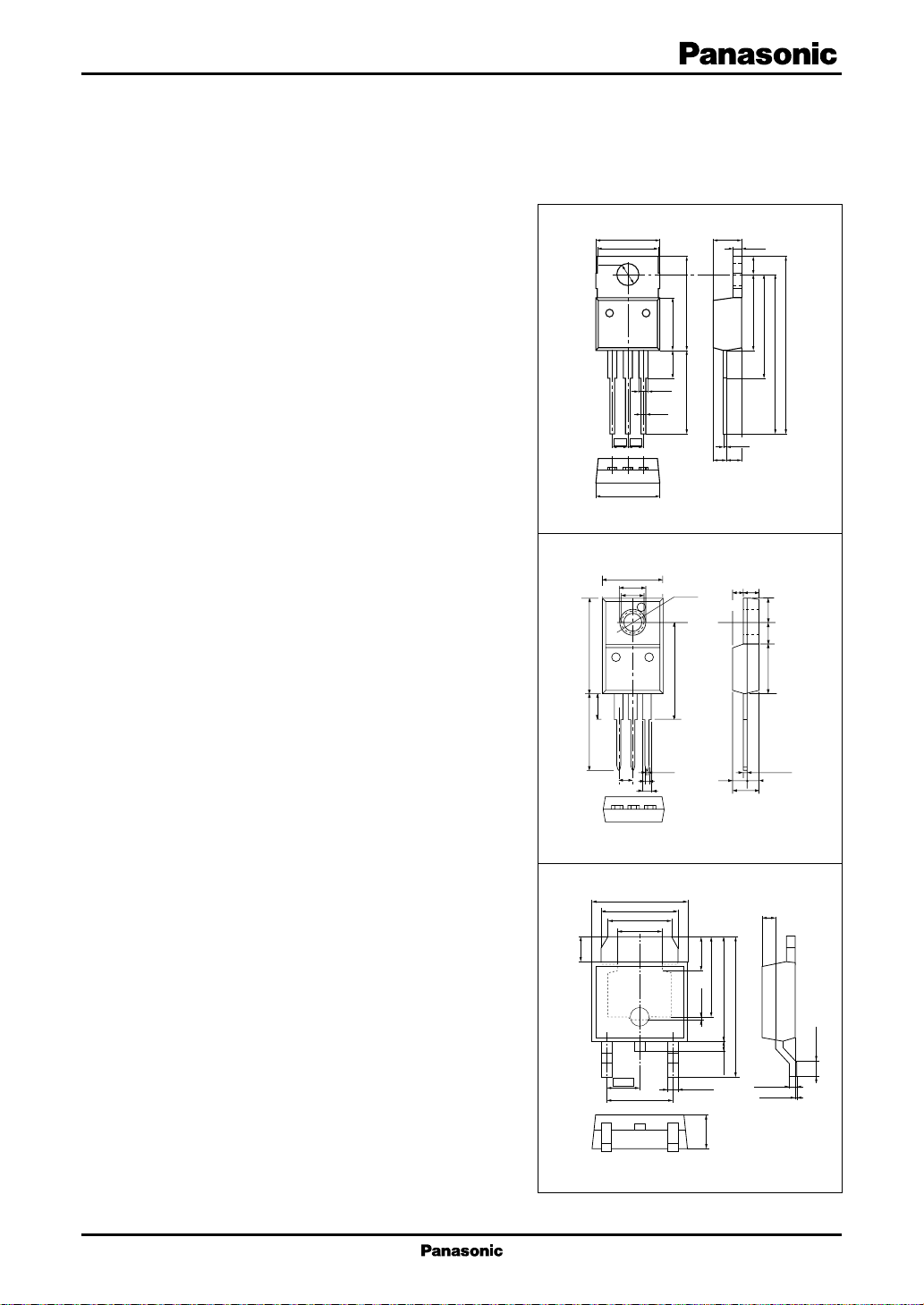
AN7700 series Unit: mm
TO-220 Package (HSIP003-P-0000)
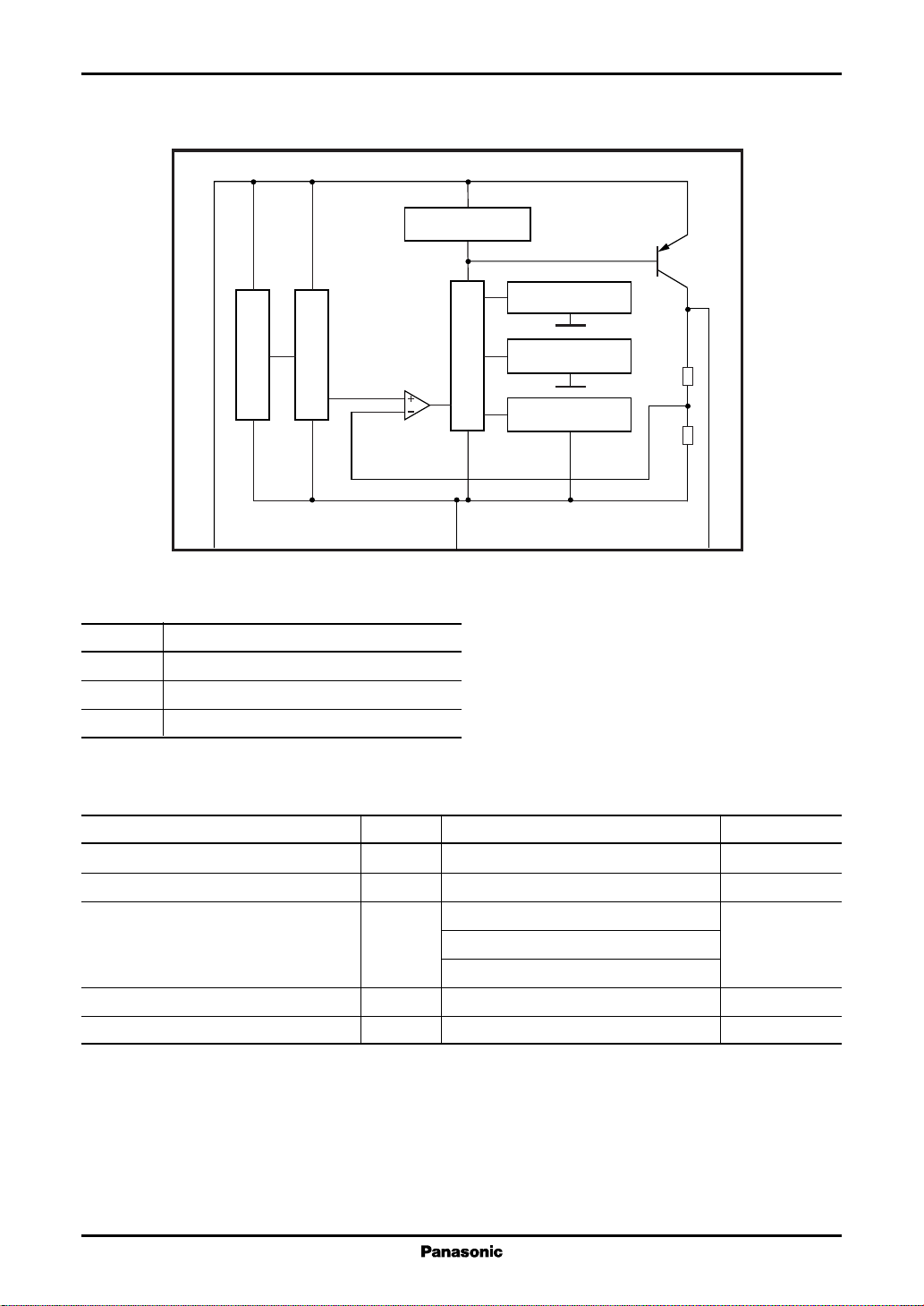
AN7700F series Unit: mm
10.5±0.3
(4.3)
4.5±0.25
13.6±0.25 16.7±0.3
φ5.3
2.54
123
(0.4)
0.8±0.2
1.4±0.2
3.1±0.1
17.0±0.25
(1.73)
2.0
±0.25
2.77±0.3
4.5±0.3
+0.1
0.4
–0.05
2.5±0.25
4.2±0.25
±0.25
8.7±0.3 3.8
TO-220F Package (HSIP003-P-0000A)
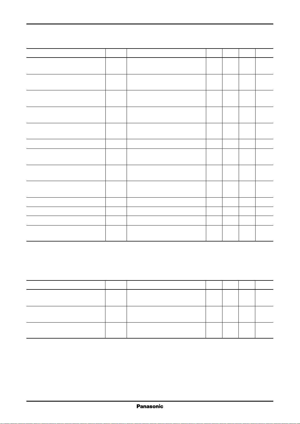
AN7700SP series Unit: mm
U-type Package
1
AN7700, AN7700F, AN7700SP Series Voltage Regulators
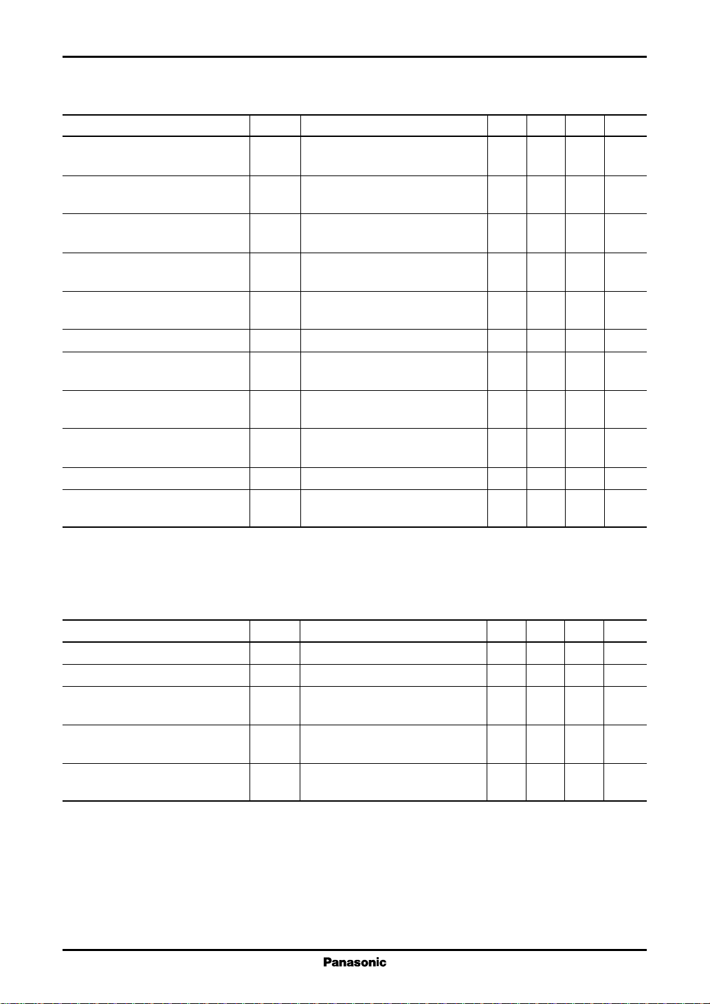
■ Block Diagram
Starter
1
■ Pin Descriptions
Pin No. Description
1 Input pin (In)
2 Ground pin (COM)
3 Output pin (Out)
V
REF
Voltage reference
Error amplifier
Input short-circuit
protection
Output driver
2
Output stage
Overcurrent
limiter
Inrush current
protection
R1
Thermal
protection
R2
3
■ Absolute Maximum Ratings at Ta = 25°C
Parameter Symbol Rating Unit
2
Supply voltage
Supply current
Power dissipation
Operating ambient temperature
Storage temperature
Note)*1: Expect for the operating ambient temperature, and storage temperature, all ratings are for Ta = 25°C.
2: At the application of VIN = 30 V, the overvoltage protection may be operated by the ASO protection circuit, leading to the
*
output shut down.
3: The current value does not exceed this criterion because of the on-chip current limiter.
*
4: The internal circuit shuts off the output when Tj ≥ 150°C (designed value). The relationship between the IC power
*
dissipation and ambient temperature shall conform to the derating curve (■ Characteristic curve chart PD Ta).
2
*
3
*
4
*
AN7700 series P
V
IN
I
IN
D
AN7700F series 10.25
AN7700SP series 5.0
1
*
1
*
T
opr
T
stg
30 V
2.4 A
15 W
−30 to +85 °C
−55 to +150 °C

Voltage Regulators AN7700, AN7700F, AN7700SP Series
■ Recommended Operating Conditions at I
Part No. Output voltage Operating supply voltage range (VIN) Unit
AN7703/F 3 4 to 14 V
AN77033SP 3.3 4.3 to 14 V
AN77035SP 3.5 4.5 to 14 V
AN7704/F 4 5 to 15 V
AN7705/F/SP 5 6 to 16 V
AN7706/F/SP 6 7 to 17 V
AN7707/F/SP 7 8 to 18 V
AN7708/F/SP 8 9 to 19 V
AN7709/F/SP 9 10 to 20 V
AN7710/F/SP 10 11 to 21 V
AN7712/F/SP 12 13 to 23 V
AN7715/F/SP 15 16.5 to 26.5 V
AN7718/F 18 19.5 to 29.5 V
AN7720/F 20 21.5 to 29.5 V
AN7724/F 24 25.5 to 29.5 V
= 500 mA, Ta = 25°C
OUT
3
AN7700, AN7700F, AN7700SP Series Voltage Regulators
■ Electrical Characteristics at Ta = 25°C
• AN7703/F (3-V type)
Parameter Symbol Conditions Min Typ Max Unit
Output voltage V
OUTVIN
= 4 V, I
Tj = 25°C
Line regulation REG
INVIN
= 4 V to 14 V, I
Tj = 25°C
Load regulation REG
LOAVIN
= 4 V, I
Tj = 25°C
Input dependency of bias current ∆I
Bias(IN)VIN
= 4 V to 14 V, I
Tj = 25°C
Load dependency of bias current ∆I
Bias(LOA)VIN
= 4 V, I
Tj = 25°C
Bias current at no load I
Bias current I
Bias
rush
VIN = 4 V, I
VIN = 2.7 V, I
before the regulation starts
Minimum I/O voltage difference 1 V
DIF(min)1VIN
= 3.5 V, I
Tj = 25°C
Minimum I/O voltage difference 2 V
DIF(min)2VIN
= 3.5 V, I
Tj = 25°C
Peak output current 1
Peak output current 2
Peak output current 3
Ripple rejection ratio RR V
*
*
*
I
O(Peak)1VIN
I
O(Peak)2VIN
I
O(Peak)3VIN
= 4 V, Tj = 25°C 1.2 1.8 2.4 A
= 13 V, Tj = 25°C 1.0 1.5 2.0 A
= 18 V, Tj = 25°C 0.5 1.0 1.5 A
= 4 V to 6 V, I
IN
f = 120 Hz
Note)*: This current exceeds P
it shall conform to the derating curve ( ■ Characteristic curve chart PD Ta ).
because it is a parameter during abnormal (overcurrent) operation. However, normally,
D(max)
= 500 mA, 2.91 3.00 3.09 V
OUT
= 500 mA, 330mV
OUT
= 0 mA to 1 200 mA, 15 60 mV
OUT
= 500 mA, 110mA
OUT
= 0 mA to 1 200 mA, 10 50 mA
OUT
= 0 mA 2.6 5.0 mA
OUT
= 0 mA 35mA
OUT
= 500 mA, 0.4 0.6 V
OUT
= 1 200 mA, 0.5 1.0 V
OUT
= 100 mA, 54 74 dB
OUT
• Design reference data
Note) The characteristics listed below are theoretical values based on the IC design and are not guaranteed.
Parameter Symbol Conditions Min Typ Max Unit
Output short-circuit current I
O(Short)VIN
= 30 V, Tj = 25°C 10 mA
The load is shorted.
Thermal protection operating T
j(TH)VIN
= 4 V 150 °C
temperature
Output voltage temperature a V
= 5 V, Tj = 25°C to 125°C −40 ppm/°C
IN
coefficient
4
Voltage Regulators AN7700, AN7700F, AN7700SP Series
■ Electrical Characteristics at Ta = 25°C (continued)
• AN77033SP (3.3-V type)
Parameter Symbol Conditions Min Typ Max Unit
Output voltage V
OUTVIN
= 4.3 V, I
Tj = 25°C
Line regulation REG
Load regulation REG
Input dependency of bias current ∆I
Load depndency of bias current ∆I
Bias current at no load I
Bias current I
Bias(IN)VIN
Bias(LOA)VIN
Bias
rush
LOAVIN
= 4.3 V to 14.3 V, 335mV
INVIN
I
= 500 mA, Tj = 25°C
OUT
= 4.3 V, 15 70 mV
I
= 0 mA to 1 200 mA, Tj = 25°C
OUT
= 4.3 V to 14.3 V, 110mA
I
= 500 mA, Tj = 25°C
OUT
= 4.3 V, 10 50 mA
I
= 0 mA to 1 200 mA, Tj = 25°C
OUT
VIN = 4.3 V, I
VIN = 3.0 V, I
before the regulation starts
Minimum I/O voltage difference 1 V
DIF(min)1VIN
= 3.7 V, I
Tj = 25°C
Minimum I/O voltage difference 2 V
DIF(min)2VIN
= 3.7 V, I
Tj = 25°C
Peak output current 1
Ripple rejection ratio RR V
Note)*: This current exceeds P
it shall conform to the derating curve ( ■ Characteristic curve chart PD Ta ).
*
D(max)
I
O(Peak)1VIN
because it is a parameter during abnormal (overcurrent) operation. However, normally,
= 4.3 V, Tj = 25 °C 1.2 1.8 2.4 A
= 4.3 V to 8.0 V, 53 74 dB
IN
I
= 100 mA, f = 120 Hz
OUT
= 500 mA, 3.20 3.30 3.40 V
OUT
= 0 mA 2.6 5.0 mA
OUT
= 0 mA 35mA
OUT
= 500 mA, 0.4 0.6 V
OUT
= 1 200 mA, 0.5 1.0 V
OUT
• Design reference data
Note) The characteristics listed below are theoretical values based on the IC design and are not guaranteed.
Parameter Symbol Conditions Min Typ Max Unit
Peak output current 2
Peak output current 3
Output short-circuit current I
*
*
I
O(Peak)2VIN
I
O(Peak)3VIN
O(Short)VIN
= 13.3 V, Tj = 25°C 1.5 A
= 18.3 V, Tj = 25°C 1.0 A
= 30 V, Tj = 25°C 10 mA
The load is shorted.
Thermal protection operating T
j(TH)VIN
= 4.3 V 150 °C
temperature
Output voltage temperature a V
= 4.3 V, Tj = 25°C to 125°C −40 ppm/°C
IN
coefficient
Note)*: This current exceeds P
it shall conform to the derating curve ( ■ Characteristic curve chart PD Ta ).
because it is a parameter during abnormal (overcurrent) operation. However, normally,
D(max)
5
AN7700, AN7700F, AN7700SP Series Voltage Regulators
■ Electrical Characteristics at Ta = 25°C (continued)
• AN77035SP (3.5-V type)
Parameter Symbol Conditions Min Typ Max Unit
Output voltage V
OUTVIN
= 4.5 V, I
Tj = 25°C
Line regulation REG
Load regulation REG
Input dependency of bias current ∆I
Load dependency of bias current ∆I
Bias current at no load I
Bias current I
Bias(IN)VIN
Bias(LOA)VIN
Bias
rush
LOAVIN
= 4.5 V to 14.5 V, 335mV
INVIN
I
= 500 mA, Tj = 25°C
OUT
= 4.5 V, 15 70 mV
I
= 0 mA to 1 200 mA, Tj = 25°C
OUT
= 4.5 V to 14.5 V, 110mA
I
= 500 mA, Tj = 25°C
OUT
= 4.5 V, 10 50 mA
I
= 0 mA to 1 200 mA, Tj = 25°C
OUT
VIN = 4.5 V, I
VIN = 3.2 V, I
before the regulation starts
Minimum I/O voltage difference 1 V
DIF(min)1VIN
= 3.7 V, I
Tj = 25°C
Minimum I/O voltage difference 2 V
DIF(min)2VIN
= 3.7 V, I
Tj = 25°C
Peak output current 1
Ripple rejection ratio RR V
Note)*: This current exceeds P
it shall conform to the derating curve ( ■ Characteristic curve chart PD Ta ).
*
D(max)
I
O(Peak)1VIN
because it is a parameter during abnormal (overcurrent) operation. However, normally,
= 4.5 V, Tj = 25°C 1.2 1.8 2.4 A
= 4.5 V to 8.0 V, 53 74 dB
IN
I
= 100 mA, f = 120 Hz
OUT
= 500 mA, 3.39 3.50 3.61 V
OUT
= 0 mA 2.6 5.0 mA
OUT
= 0 mA 35mA
OUT
= 500 mA, 0.4 0.6 V
OUT
= 1 200 mA, 0.5 1.0 V
OUT
• Design reference data
Note) The characteristics listed below are theoretical values based on the IC design and are not guaranteed.
Parameter Symbol Conditions Min Typ Max Unit
Peak output current 2
Peak output current 3
Output short-circuit current I
*
*
I
O(Peak)2VIN
I
O(Peak)3VIN
O(Short)VIN
= 13.5 V, Tj = 25°C 1.5 A
= 18.5 V, Tj = 25°C 1.0 A
= 30 V, Tj = 25°C 10 mA
The load is shorted.
Thermal protection operating T
j(TH)VIN
= 4.5 V 150 °C
temperature
Output voltage temperature a V
= 4.5 V, Tj = 25°C to 125°C −40 ppm/°C
IN
coefficient
Note)*: This current exceeds P
it shall conform to the derating curve ( ■ Characteristic curve chart PD Ta ).
because it is a parameter during abnormal (overcurrent) operation. However, normally,
D(max)
6

Voltage Regulators AN7700, AN7700F, AN7700SP Series
■ Electrical Characteristics at Ta = 25°C (continued)
• AN7704/F (4-V type)
Parameter Symbol Conditions Min Typ Max Unit
Output voltage V
OUTVIN
= 5 V, I
Tj = 25°C
Line regulation REG
INVIN
= 5 V to 15 V, I
Tj = 25°C
Load regulation REG
LOAVIN
= 5 V, I
Tj = 25°C
Input dependency of bias current ∆I
Bias(IN)VIN
= 5 V to 15 V, I
Tj = 25°C
Load dependency of bias current ∆I
Bias(LOA)VIN
= 5 V, I
Tj = 25°C
Bias current at no load I
Bias current I
Bias
rush
VIN = 5 V, I
VIN = 3.6 V, I
before the regulation starts
Minimum I/O voltage difference 1 V
DIF(min)1VIN
= 3.6 V, I
Tj = 25°C
Minimum I/O voltage difference 2 V
DIF(min)2VIN
= 3.6 V, I
Tj = 25°C
Peak output current 1
Peak output current 2
Peak output current 3
Ripple rejection ratio RR V
*
*
*
I
O(Peak)1VIN
I
O(Peak)2VIN
I
O(Peak)3VIN
= 5 V, Tj = 25°C 1.2 1.8 2.4 A
= 14 V, Tj = 25°C 1.5 A
= 19 V, Tj = 25°C 1.0 A
= 5 V to 7 V, I
IN
f = 120 Hz
Note)*: This current exceeds P
it shall conform to the derating curve ( ■ Characteristic curve chart PD Ta ).
because it is a parameter during abnormal (overcurrent) operation. However, normally,
D(max)
= 500 mA, 3.88 4.00 4.12 V
OUT
= 500 mA, 440mV
OUT
= 0 mA to 1 200 mA, 20 80 mV
OUT
= 500 mA, 1.0 10 mA
OUT
= 0 mA to 1 200 mA, 10 50 mA
OUT
= 0 mA 2.6 5.0 mA
OUT
= 0 mA 35mA
OUT
= 500 mA, 0.4 0.6 V
OUT
= 1 200 mA, 0.5 1.0 V
OUT
= 100 mA, 52 72 dB
OUT
• Design reference data
Note) The characteristics listed below are theoretical values based on the IC design and are not guaranteed.
Parameter Symbol Conditions Min Typ Max Unit
Output short-circuit current I
O(Short)VIN
= 30 V, Tj = 25°C 10 mA
The load is shorted.
Thermal protection operating T
j(TH)VIN
= 5 V 150 °C
temperature
Output voltage temperature a V
= 5 V, Tj = 25°C to 12°C −40 ppm/°C
IN
coefficient
7
 Loading...