

Panasonic AN7561Z Datasheet
ICs for Audio Common Use
AN7561Z
BTL output power IC for car audio
■ Overview
The AN7561Z is an audio power IC developed as a car
audio output (35 W × 4-ch). CR to stop oscillation is built
in between the output pin and GND so that a space saving of set is possible. Also, it is incorporating a perfect
muting circuit which does not make a shock noise so that
a shock noise design in the set transitional state can be
made easily when used together with its standby function. In addition, it is incorporating various protective
circuits to protect the IC from destruction by GND-open
earth short-circuiting and power supply surge which are
the important subject of power IC, and the IC will largely
contribute to a high reliability design of equipment.
■ Features
• Pin arrangement which does not allow the input/output
patterns to intersect each other so that it is possible to
make a pattern design on a one-sided printed circuit
board.
• Incorporating various protection circuits (thermal pro-
tection, short-circuit to V
opened, short-circuit to GND, short-circuit to GND in
GND-opened, over voltage, power supply surge, and
ASO protection, etc.)
• Incorporating standby function (shock noise-free at STB-
on/off)
• Incorporating standby function (shock noise-free at
Mute-on/off)
• External components reduction
• Provided with beep sound input pin
• Equipped with auxiliary sound input pin
• Inverted pin layout of AN7560Z on right and left pins
, short-circuit to VCC in VCC-
CC
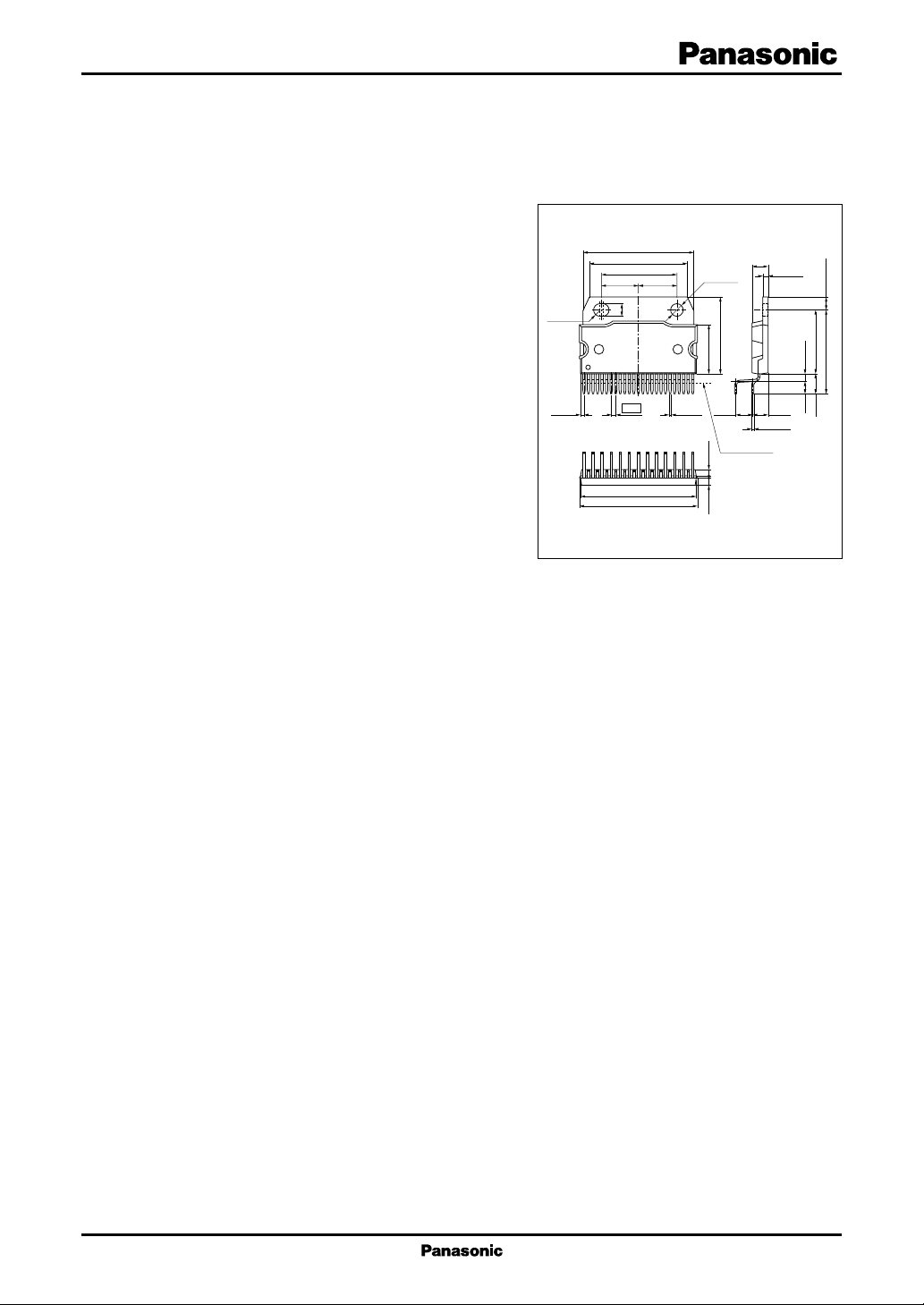
31.0±0.3
27.0±0.3
21.0±0.1
(10.50)(10.50)
R1.8±0.1
125
(1.26)
3.6±0.1
1.27
33.0±0.3
33.36±0.30
+0.2
0.6
–0.1
4.5±0.2
φ3.6±0.1
15.5±0.3
14.5±0.3(1.95) (2.15)
(5.08) (4.29)
Seating plane
HZIP025-P-0980
Unit: mm
1.5±0.1
+0.15
0.40
–0.05
(3.30) 2.4±0.5
(5.70) 18.75±0.30
(24.45) 3.75±0.10
■ Applications
• Car stereo, miniature audio component, karaoke and
other audio equipment.
1
AN7561Z ICs for Audio Common Use
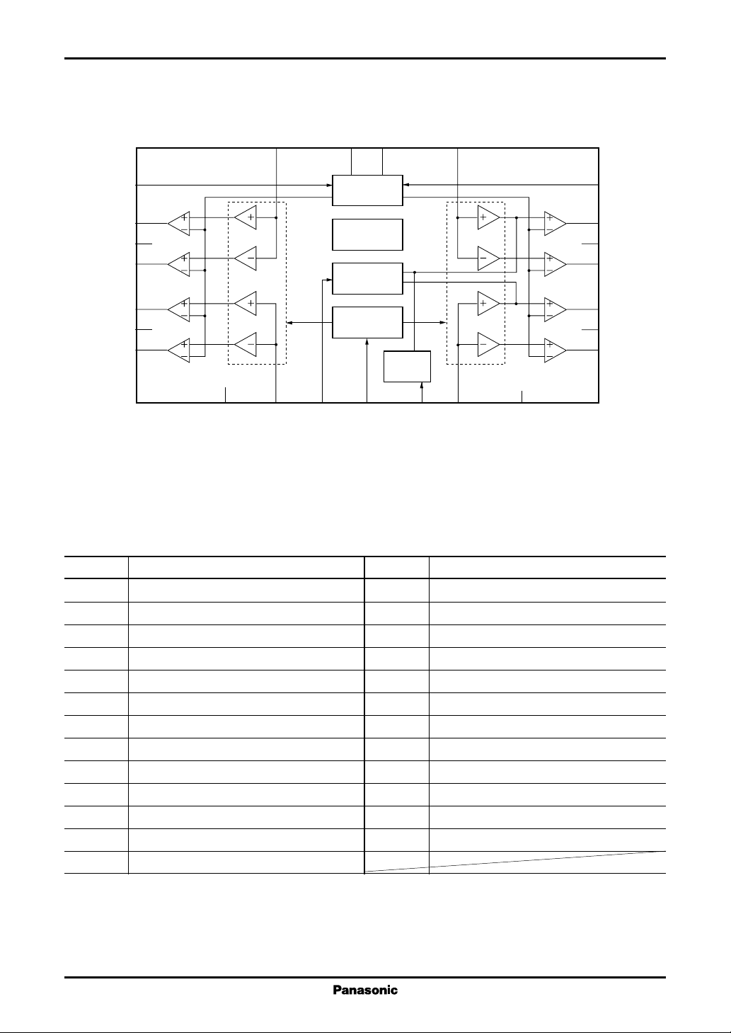
■ Block Diagram
CCVCC
GND (Output)
GND (Output)
V
5
1
25
24
23 15
21
20
19
6
3
8
22
14
Ripple
Filter
Protection
Circuit
Beep
Input
Attenuation
Control
2
AUX
Input
7
10
17
18
GND (Output)
13
12
GND (Output)
11
AttenuatorAttenuator
9
16
4
GND (Input)
Beep
Muting
AUX
■ Pin Descriptions
Pin No. Description
1 Ripple filter
2 Mute
3 ch.3 input
4 GND (Sub)
5 ch.4 input
6 GND (Input)
7 ch.2 input
8 Beep input
9 ch.1 input
10 Standby
11 ch.1 − output
12 GND (ch.1 output)
13 ch.1 + output
Note) The output pin requires no capacitor and resistor for oscillation prevention.
If those are required for countermeasure against noise, be sure to use after confirmation.
Pin No. Description
14 Supply voltage V
15 ch.2 − output
16 AUX input
17 ch.2 + output
18 GND (ch.2 output)
19 ch.3 − output
20 GND (ch.3 output)
21 ch.3 + output
22 Supply voltage V
23. ch.4 − output
24 GND (ch.4 output)
25 ch.4 + output
GND (Sub)
CC
CC
2
ICs for Audio Common Use AN7561Z
■ Absolute Maximum Ratings
Parameter Symbol Rating Unit
2
Supply voltage
Peak power-supply-voltage
Supply current I
Power dissipation
Operating ambient temperature
Storage temperature
Note) *1:Ta = 25 °C except power dissipation, operating ambient temperature and storage temperature.
*2: Without signal
*3: Time = 0.2 s
*4:Ta = 85 °C
■ Recommended Operating Range
Supply voltage V
*
3
*
4
*
1
*
1
*
V
V
Surge
P
T
T
CC
CC
opr
stg
25 V
65 V
12 A
D
59 W
−30 to +85 °C
−55 to +150 °C
Parameter Symbol Range Unit
CC
8.0 to 18.0 V
■ Electrical Characteristics at VCC = 13.2 V, freq = 1 kHz, Ta = 25°C
Parameter Symbol Conditions Min Typ Max Unit
Quiescent circuit current I
Standby current I
1
Output noise voltage
*
Voltage gain G
Total harmonic distortion 1 THD1 VIN = 40 mV, RL = 4 Ω0.05 0.2 %
Maximum output power P
1
Ripple rejection ratio
*
Channel balance CB VIN = 40 mV, RL = 4 Ω01dB
Crosstalk CT V
Output offset voltage V
1
Muting effect
*
Input impedance Z
2
Shock noise
Note) *1: Use 15 Hz to 30 kHz (12 dB/OCT) band-pass filter at measurement.
*2: Change over the standby pin at 0V and 5V with the following time.
*
Standby pin voltage
5 V
RG = 10 kΩ, RL = 4 Ω300 450 mA
CQ
RG = 10 kΩ, RL = 4 Ω110µA
STB
V
RG = 10 kΩ, RL = 4 Ω0.15 0.5
NO
VIN = 40 mV, RL = 4 Ω 32 34 36 dB
V
THD = 10%, RL = 4 Ω 16.0 19.5 W
O
mV[rms]
RR RL = 4 Ω, RG = 10 kΩ,6068 dB
VR = 1 V[rms], fr = 1 kHz
= 40 mV, RL = 4 Ω6070dB
IN
RG = 10 kΩ
RG = 10 kΩ, RL = 4 Ω−250 0 250 mV
OFF
MT VIN = 40 mV, RL = 4 Ω 70 86 dB
VIN = ±0.3 V
I
V
RL = 4 Ω, RG = 10 kΩ, −100 0 100 mV[p-0]
S
V
MUTE
DC
= 5 V, V
= On/Off
STB
24 30 36 kΩ
50 Hz HPF
0 V
500 ms 500 ms
3
AN7561Z ICs for Audio Common Use
■ Electrical Characteristics at VCC = 9 V, Ta = 25 °C (continued)
Parameter Symbol Conditions Min Typ Max Unit
Total harmonic distortion 2 THD2 V
Mute-on threshold voltage MT
Mute-off threshold voltage MT
Cutoff frequency f
ONVIN
OFFVIN
C
• Design reference data at VCC = 13.2 V, f = 1 kHz, measuring bandwidth 15 Hz to 30 kHz (12 dB/OCT) filter
is used
Note) The characteristic values below are theoretical values for designing and not guaranteed.
Parameter Symbol Conditions Min Typ Max Unit
Maximum output power P
Maximum output power P
Maximum output power P
Power band f
Power band f
STB threshold voltage V
STB threshold voltage V
Omax
O2
Omax2VCC
PL
PH
STB1RG
STB2RG
= 20 mV, fIN = 20 kHz, 0.1 0.5 %
IN
RG = 10 Ω, RL = ∞
= 40 mV, RL = 4 Ω 4 V
= 40 mV, RL = 4 Ω0.8 V
VIN = 40 mV, RL = 4 Ω 20 40 kHz
GV = −1 dB (0 dB: 1 kHz)
max. power, RL = 4 Ω28 W
VCC = 14.4 V, THD = 10%,21 W
RL = 4 Ω
= 14.4 V, max. power,34 W
RL = 4 Ω
VCC = 14.4 V, THD = 1%,10 Hz
R
= 4 Ω,
L
POL = −3 dB (1 kHz: 0 dB)
VCC = 14.4 V, THD = 1%,18 kHz
RL = 4 Ω,
POH = −3 dB (1 kHz: 0 dB)
= 10 kΩ, RL = 4 Ω, 2.2 V
STB→ACT
= 10 kΩ, RL = 4 Ω, 1.5 V
ACT→STB
4
 Loading...