

Panasonic AN7535NSA Datasheet
ICs for Audio Common Use
AN7535NSA
Headphone amplifier IC
for portable equipment
■ Overview
The AN7535NSA is an audio signal processing
IC in which line amplifiers and beep circuit are built
in the headphone amplifiers for use in portable
equipment. Its headphone output block is using the
center amplifier method which eliminates the need
for coupling capacitor so that the circuit is most
suitable for rationalization of audio circuit.
■ Features
• Output coupling capacitor is not required (Center
amplifier method)
• Built-in line amplifiers
• Built-in headphone amplifier gain change-over
circuit (8 dB/12 dB)
• Built-in mute circuit
• Built-in beep circuit
• Built-in circuit against a shock noise generated
when power supply is momentary cut off.
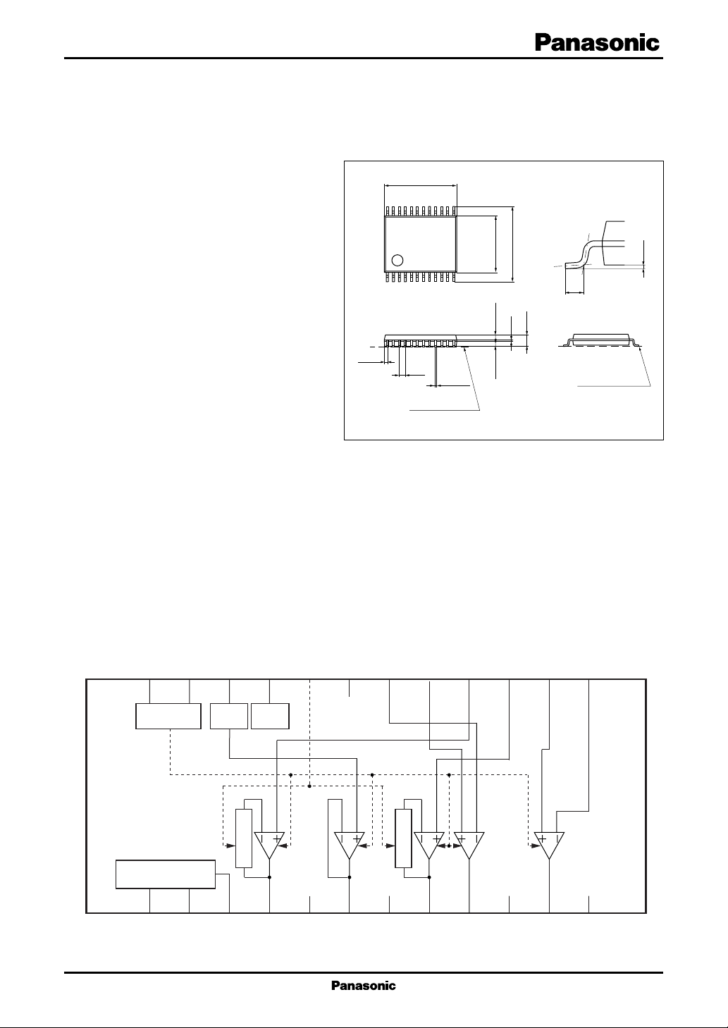
7.8
±0.3
24 13
112
(0.325)
0.65
0.22
Seating plane
±0.3
±0.3
6.1
8.1
±0.1
±0.2
0.15
1.2
0.525
±0.1
+0.1
0.525
−0.05
SSOP024-P-0300B
Unit : mm
±0.1
0.1
(0.5)
Seating plane
■ Applications
• Potable CD and MD players, etc.
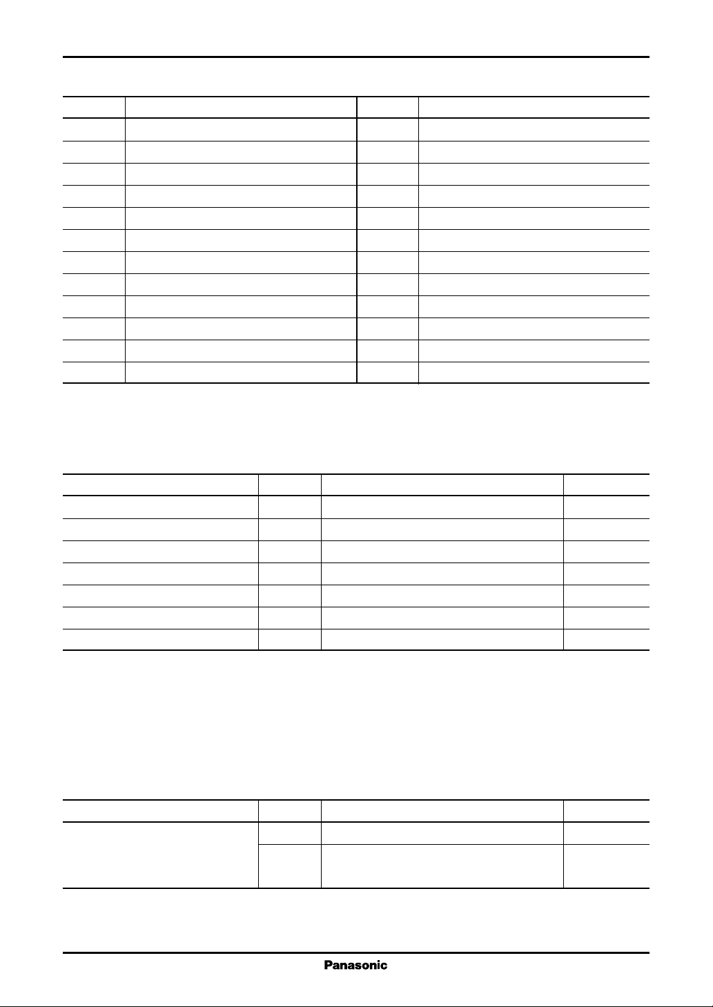
■ Block Diagram
23
2
22
REF
3
24
Mute V
Ripple Filter
1
21
Beep
8/12 dB
4
20
5
11819
6
1
7
17
8/12 dB
8
16
9
15
10
14
11
13
12
1
AN7535NSA ICs for Audio Common Use
■ Pin Descriptions
Pin No. Description
1V
CC1
2 Ripple filter
3 Supply voltage
4 Headphone amplifier ch.1 output pin
5N.C.
6 Center amplifier output pin
7 Output GND
8 Headphone amplifier ch.2 output pin
9 Line amplifier ch.1 output pin
10 Line amplifier supply voltage
11 Line amplifier ch.2 output pin
12 N.C.
Pin No. Description
13 Line amplifier ch.2 NF pin
14 Line amplifier ch.2 input pin
15 Headphone amplifier ch.2 input pin
16 Headphone amplifier ch.1 input pin
17 Line amplifier ch.1 input pin
18 Line amplifier ch.1 NF pin
19 Input GND
20
Headphone amplifier gain change-over pin
21 Beep input pin
22 Internal reference voltage
23 Mute pin
24 Mute time-constant
■ Absolute maximum ratings
Parameter Symbol Rating Unit
2
Supply voltage
Line amplifier supply voltage
Supply current I
Line amplifier supply current I
Power dissipation
Operating ambient temperature
Storage temperature
Notes)*1 : All items are at Ta = 25°C, except for the operating ambient temperature and storage temperature parameters .
*
2
*
3
*
1
*
1
*
2 : Without signal
*
3:Ta = 75°C when mounted on the recommended printed circuit board (Glass epoxy board 50 mm × 50 mm × t0.8 mm)
*
4 : Use under the condition of V
*
V
V
CC-LINE
CC-LINE
T
CC-LINE
CC
7V
7V
CC
200.0 mA
20.0 mA
P
D
opr
T
stg
≥ V
CC
370 mW
−20 to + 75 °C
−55 to + 150 °C
■ Recommended Operating Range
Parameter Symbol Range Unit
1
Supply voltage
*
V
V
CC-LINE
CC
1.8 to 3.4 V
1.8 to 3.4 V
(VCC to VCC + 0.2)
2
ICs for Audio Common Use AN7535NSA
■ Electrical Characteristics
Unless otherwise specially specified, VCC = 2.6 V, V
RL = 10 kΩ (line out), Ta = 25°C
Parameter Symbol Conditions Min Typ Max Unit
Quiescent current 1 I
Quiescent current 2 I
Quiescent current 3 I
CQM
CQ1
CQ2
HP amplifier
Voltage gain 1 G
Voltage gain 2 G
Channel balance CB VO = 0.35 V[rms], GV = 8 dB −10 1dB
Total harmonic distortion THD VO = 0.35 V[rms], GV = 8 dB 0.05 0.2 %
Maximum output power P
1
Output noise voltage
Channel cross-talk
*
2
*
V
CT VO = 0.35 V[rms], GV = 8 dB 40 45 dB
Ripple rejection RR
2
Mute attenuation
Beep sound output voltage
*
V
MUTEVIN
3
*
V
Line amplifier
Voltage gain G
Total harmonic distortion THDLVIN = −6 dBm 0.003 0.02 %
Channel cross-talk CTL VIN = −6 dBm 85 95 dB
1
Output noise voltage
Mute attenuation
*
2
*
V
V
MUTE LVIN
Mute operating voltage V
Mute release voltage V
Gain change-over operating V
MOFF
GCON
voltage 10.9 dB to 13.9 dB
Gain change-over Off voltage V
Note)*1 : Using A curve filter
2 : Using 30 kHz LPF
*
3 : The specifications are guaranteed under the both mute on/off conditions.
*
GCOFF
Mute-on 0.7 1.9 3.0 mA
Without input, pin 3 current, Mute-off 2.2 4.3 8.8 mA
Without input, pin 10 current, Mute-off
VO = 0.35 V[rms], GV = 12 dB 10.0 11.7 13.0 dB
V1
VO = 0.35 V[rms], GV = 8 dB 6.0 7.8 9.0 dB
V2
THD = 10%, GV = 8 dB 20 44 mW
O
Rg = 10 kΩ, GV = 8 dB −102 −93 dBm
NO
VR = 0.1 V[rms], fR = 100 Hz, GV = 8 dB
= −15 dBm, GV = 8 dB 70 98 dB
VIN = 2.2 dBm, GV = 8 dB 5 10 15 mV[p-p]
BEEP
VIN = −6 dBm 5.0 6.0 7.0 dB
V L
Rg = 10 kΩ −104 −98 dBm
NO L
= −15 dBm 70 80 dB
Pin 23 voltage for mute operation 0.5 V
MON
Pin 23 voltage for mute release 2.2 V
Pin 20 voltage for voltage gain 0.5 V
Pin 20 voltage for voltage gain 2.2 V
6.9 dB to 9.9 dB
= 2.8 V, f = 1 kHz, RL = 16 Ω (HP out),
CC-LINE
0.4 1.1 2.0 mA
60 77 dB
3
 Loading...