

Panasonic AN7510, AN7523, AN7522, AN7513S, AN7513 Datasheet
...
New
BTL Audio Power IC AN7510/7520 Series
■ Overview
The AN7510/7520 series is a 0.5W to 3W BTL audio power amplifier IC. Equipped with a standby function and mute or DC
volume circuit, the series includes a lineup of single and dual output models. With simplified set design due to minimum
external components, this IC has a wide variety of applications.
■ Features
• Operating power sourcs voltage: 3.0V to 13.5V.
• Built-in standby function.
• Built-in mute or DC volume circuit.
■ Specifications
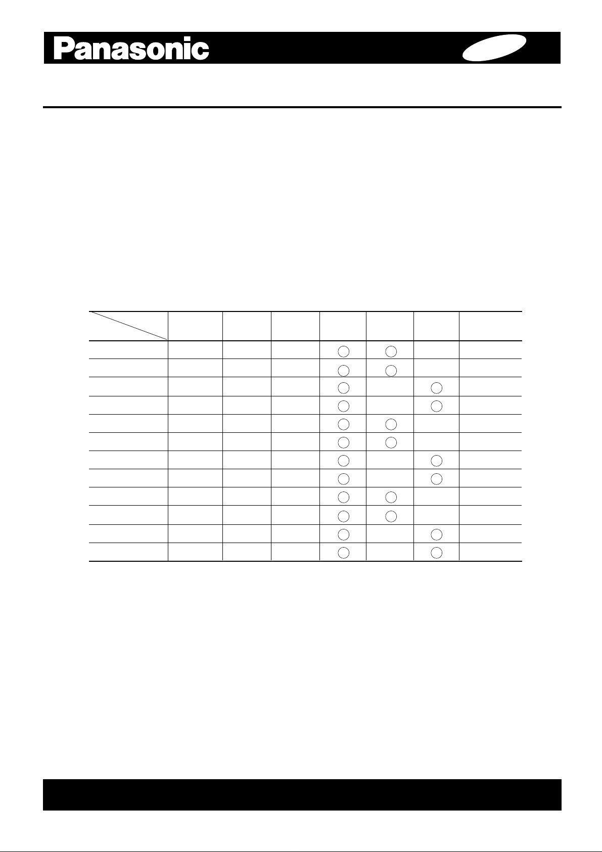
Parameters
Product
name
AN7510S
AN7511S
AN7512S
AN7513S
AN7510
AN7511
AN7512
AN7513
AN7520
*
AN7521
*
AN7522
AN7523
* : Planned
Output
power
0.5W×2ch
0.5W×1ch
0.5W×2ch
0.5W×1ch
1.0W×2ch
1.0W×1ch
1.0W×2ch
1.0W×1ch
3.0W×2ch 8V 8Ω
3.0W×1ch 8V 8Ω
3.0W×1ch 8V 8Ω
Vcc
5V
5V
5V
5V
5V
5V
5V
5V
Load
resistance
16Ω
16Ω
16Ω
16Ω
8Ω
8Ω
8Ω
8Ω
Standby Mute Volume
Package
SOP-16pin
SOP-8pin
SOP-16pin
SOP-8pin
HDIP-16pin
DIP-8pin
HDIP-16pin
DIP-8pin
HSIP-12pin
HSIP-9pin
HSIP-12pin3.0W×2ch 8V 8Ω
HSIP-9pin
■ Applications
● TVs ● Audio equipment ● Personal computers ● Active speakers
¶ The products and specifications are subject to change without any notice. Please ask for the latest product standards to guarantee the satisfaction of your product requirements.
Matsushita Electronics Corporation
1 Kotari Yakemachi, Nagaokakyo, Kyoto, 617-8520 Japan Tel. (075) 951-8151 http://www.mec.panasonic.co.jp
New publication, effective from Jan. 13 1999.
AN7510, AN7510S
1
2
3
4
5
6
7
8
10
9
11
12
13
14
15
16
27.4±0.3
6.35±0.3
4.7±0.25
1.06±0.25
3.05
±0.25
0.5±0.1
1.2±0.25
2.54±2.54
1.7
1.5±0.1
3.80±0.3
17
7.62±0.25
0 to 6
0.45
+0.1
–0.05
0.5±0.1
φ2.1
5.08±0.1
21.6±0.3
Dual 0.5,1W BTL Audio Power Amplifier Circuit
■ Features
• AN7510: Vcc=5V,Output=1W(8Ω)
• AN7510S:Vcc=5V,Output=0.5W(16Ω)
• Built-in Standby function.
• Built-in Mute circuits.
■ Applications
• TVs, Audio equipment, Personal computers,Active speakers
AN7510
AN7510S
14 13 12 11 10 91516
34567821
0.4±0.25 1.27(0.4)
10.09±0.3
HDIP016-P-0300
0.1±0.1
(0.4)
Unit : mm
Unit : mm
5.5±0.3
7.6±0.3
+0.1
–0.05
0.2
0.9±0.250.9±0.25
2.05±0.2
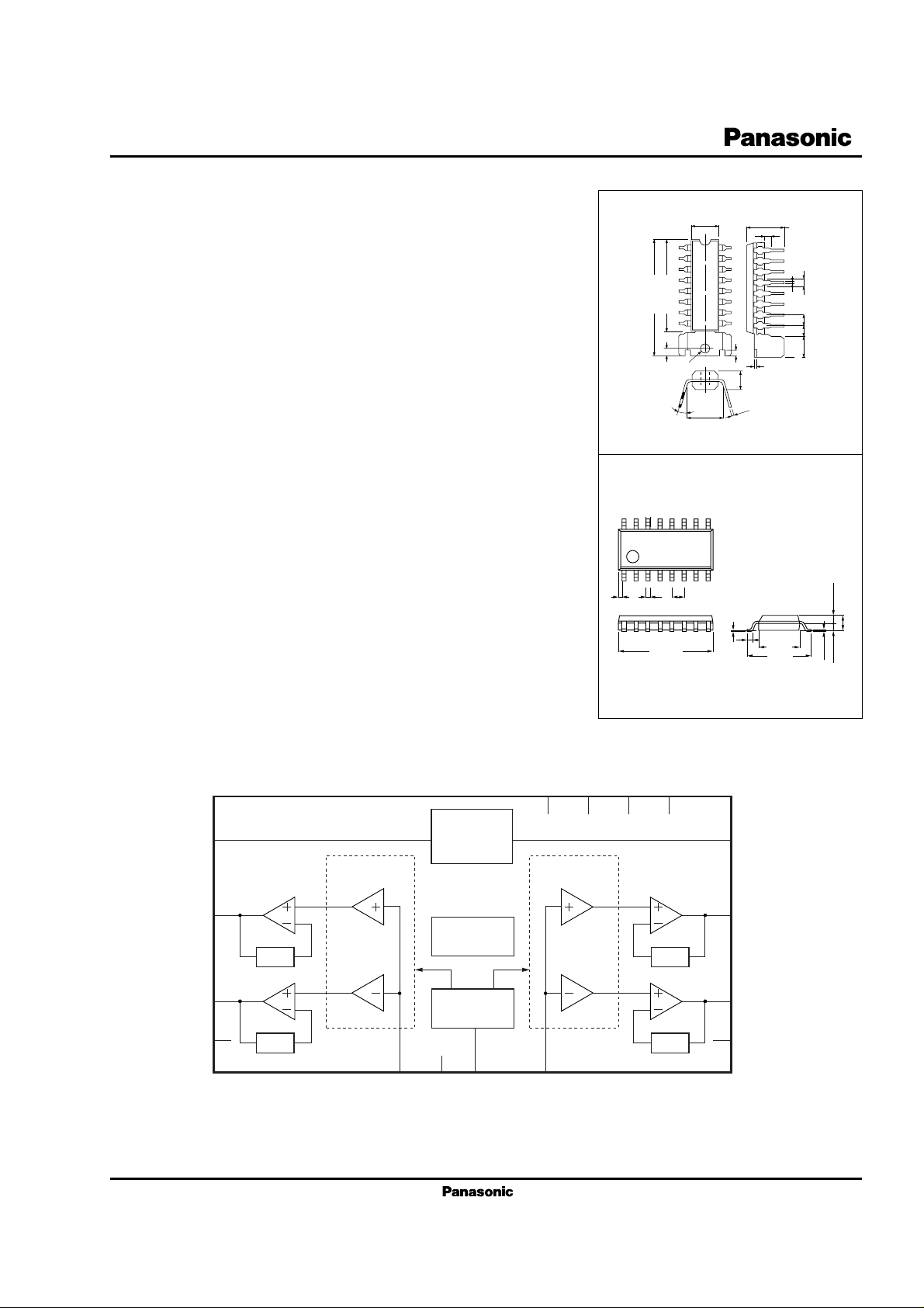
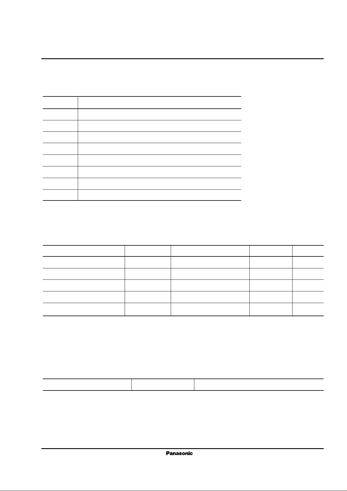
■ Block Diagram
ch.1 Output
ch.1 Output
GND
(ch.1 Output)
SOP016-P-0300
N.C.
N.C.
N.C.
N.C.
1
7
9
12
V
CC
Ripple
Rejection
Circuit
16
2
Standby
AttenuatorAttenuator
13
11
ch.2 Output
Thermal
Shutdown
28dB
8
ch.2 Output
15
28dB
Attenuator
control
14
28dB
3
ch.1 Input
4
GND
5
28dB
6
Mute
ch.2 Input
10
GND
(ch.2 Output)
■ Pin Descriptions
AN7510,7510S
Pin No.
1
2
3
4
5
6
7
8
Function
N.C
Standby
ch1 Input
GND(Input)
Mute
ch2 Input
N.C
ch2 Output(-)
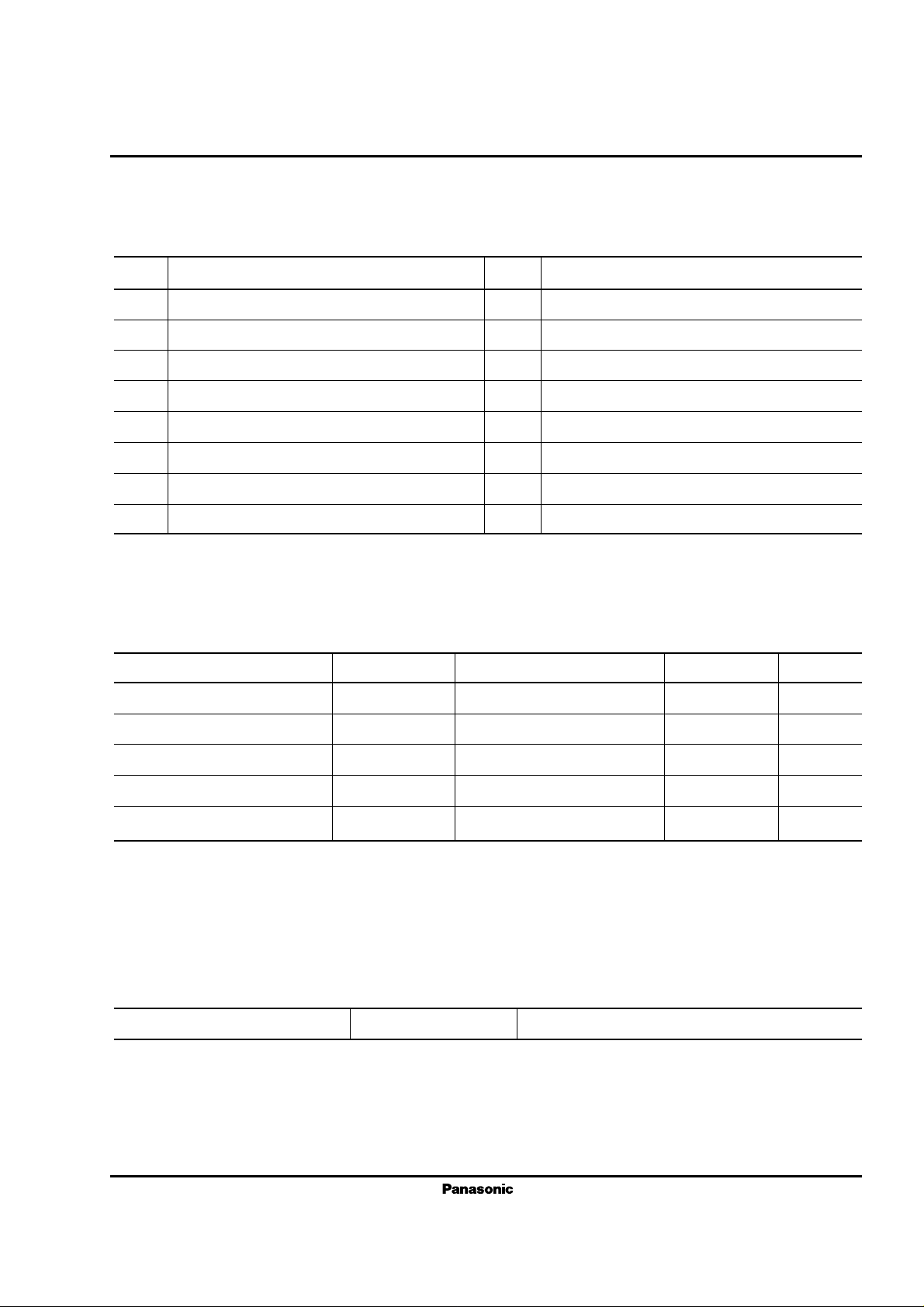
■ Absolute Maximum Ratings
Parameter
Storage temperature
Operating ambient temperature
Symbol
Tstg
Topr
Pin No.
9
10
11
12
13
14
15
16
Ratio
AN7510 -55 to +150
AN7510S -55 to +125
-25 to +70
Function
N.C
GND(Output ch2)
ch2 Output(+)
Vcc
ch1 Output(+)
GND(Output ch1)
ch1 Output(-)
N.C
Unit
ºC
ºC
Note
1
1
Supply voltage
Supply current
Power dissipation
Note1) Ta=25ºC except storage temperature and operating ambient temperature.
Note2) At no-signal.
Vcc
Icc
PD
AN7510 1127
AN7510S 236
14
2.0
■ Operating Supply Voltage Range
Operating supply voltage range
Vcc
mW
3.5V to 13.5V
V
A
2
Ta=70ºC
■ Electrical Characteristics (Vcc=5.0V,RL=8Ω,freq=1kHz,Ta=25ºC ±2 ºC)
AN7510,7510S
Parameter
Quiescent current
Standby current
Output noise voltage
Voltage gain
Total harmonic distortion
Maximum power output
Ripple rejection ratio
Output offset voltage
Muting effect
Channel balance
Channel crosstalk
Symbol
ICQ
ISTB
VNO
GV
THD
PO
RR
Voff
MT
CB
CT
Condition
VIN=0mV
VIN=0mV
Rg=10kΩ
PO=0.25W
PO=0.25W
THD=10%
Rg=10kΩ
Vr=1Vrms,fr=120Hz
Rg=10kΩ
PO=0.25W
PO=0.25W
PO=0.25W
min.
–
–
–
32
–
0.8
30
-300
70
-1
55
Note1) For this measurement,use the filter <Bandwidth:15Hz to 30kHz(12dB/octave)>
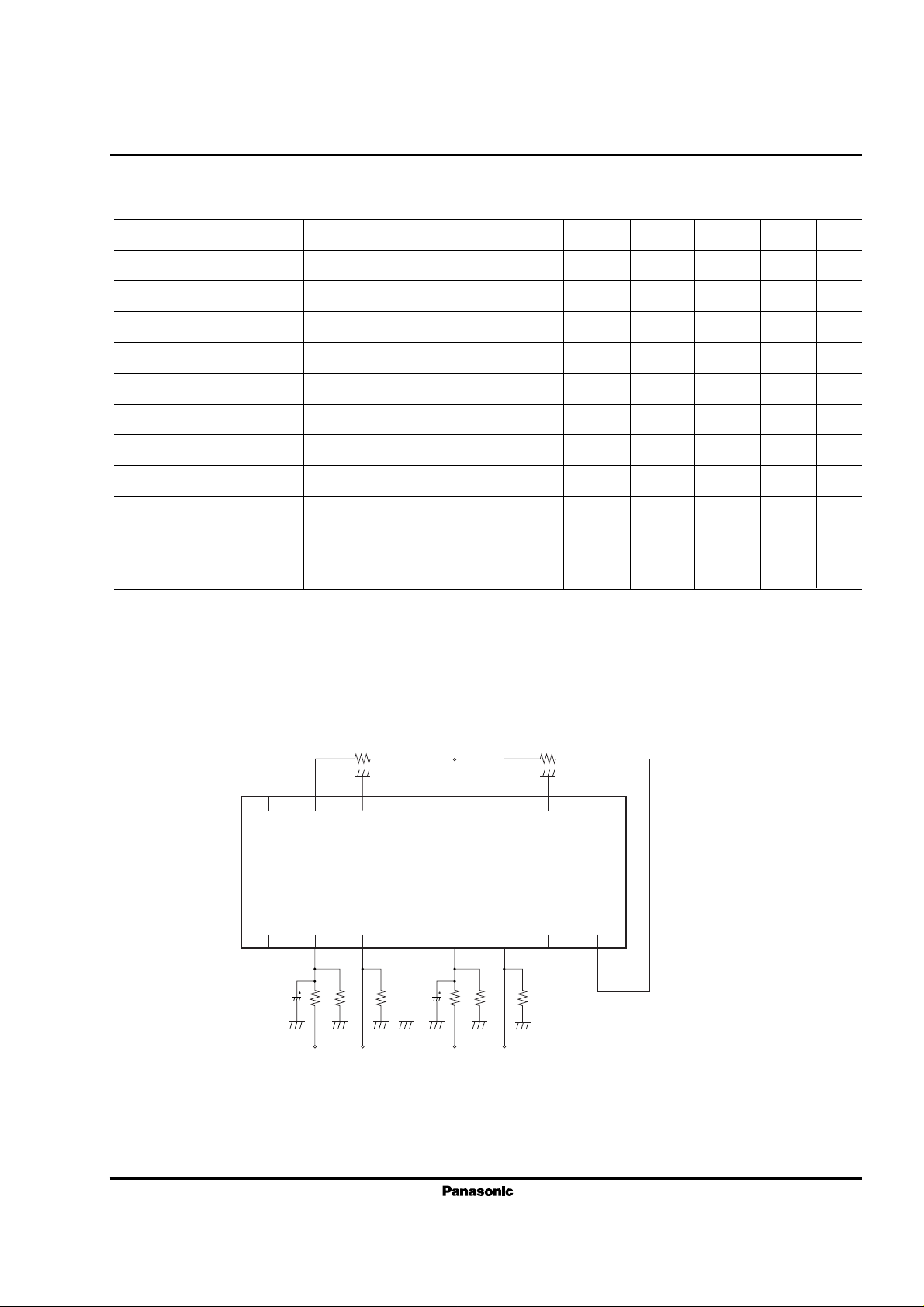
■ Application Circuit
typ.
50
1
0.14
34
0.05
1.1
50
0
86
0
65
max.
100
10
0.4
36
0.5
–
–
300
–
1
–
Unit
mA
µA
mVrms
dB
%
W
dB
mV
dB
dB
dB
Note
1
1
1
16
1
15
2
10µF
Standby V
Out1
8Ω
14
3
68kΩ
10kΩ
270kΩ
IN1
V
CC
13
12
4
5
47kΩ
1.0µF
Mute
Out2
8Ω
10
11
7
6
10kΩ
100kΩ
V
IN2
9
8
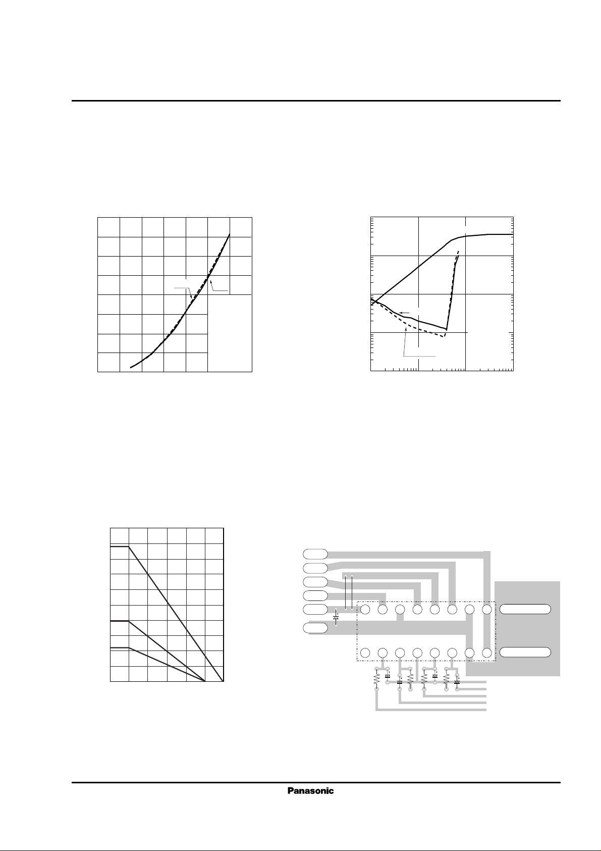
■ Characteristic Curve(AN7510)
PO - VCC PO,THD - VIN
AN7510,7510S
8
7
6
(W)
5
O
4
3
Output Power P
2
1
0
02468101214
ch.2
ch.1
freq=1kHz
THD=10%
R
L
400Hz HPF
30kHz LPF
2-ch Input
R
g
V
STB
V
MUTE
Supply Voltage VCC (V)
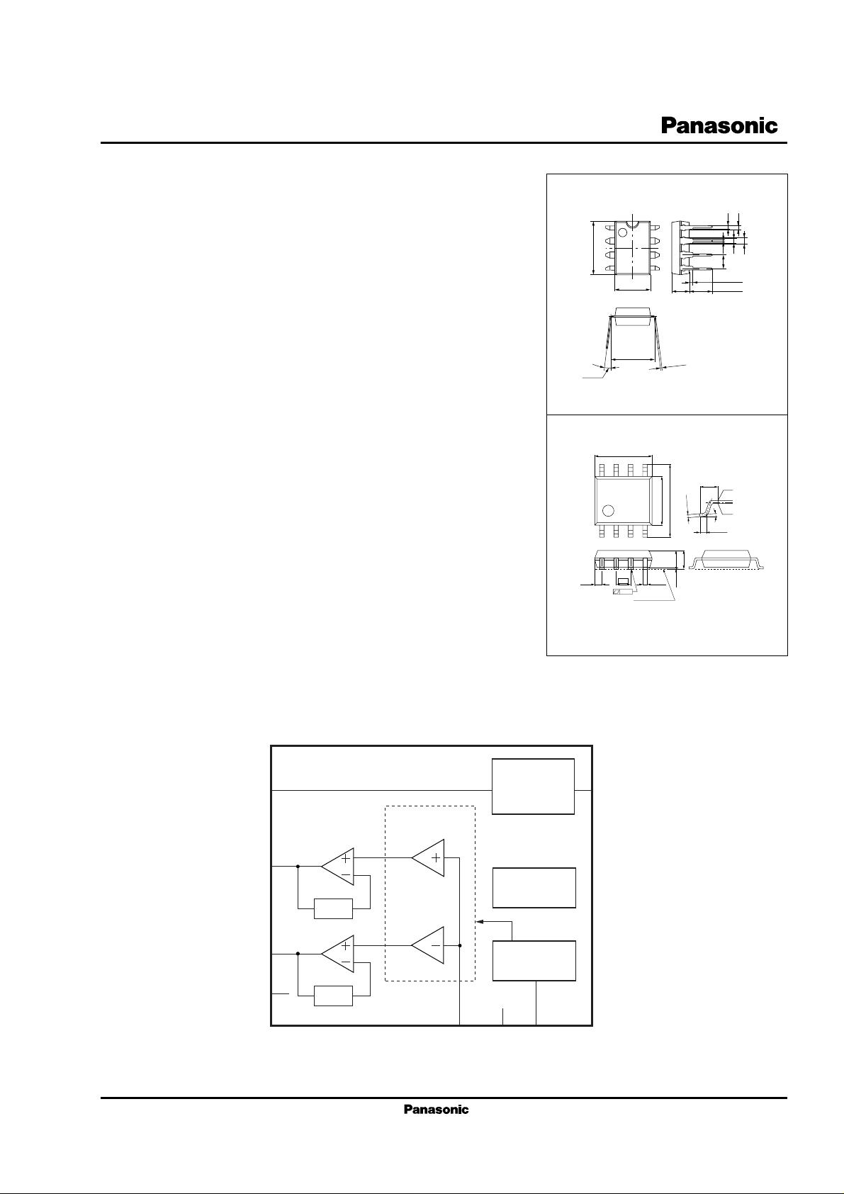
■ Package Power Dissipation
=8Ω
=10kΩ
=5V
=0V
10
1
(W)
O
0.1
THD(10kHz)
Output Power P
0.01
THD(1kHz)
0.001
1 10 100 1000
Input Voltage VIN (mV
■ Printed Board Circuit Layout
PO(ch.1),PO(ch.2)
VCC=5V
freq=1kHz
=8Ω
R
L
400Hz HPF
30kHz LPF
2-ch Input
=10kΩ
R
g
V
=5V
STB
=0V
V
MUTE
)
rms
100
10
1
0.1
Total Harmonic Distortion THD (%)
0.01
2000
1
1800
1600
1400
(mW)
D
1200
1000
2
800
600
3
Power Dissipation P
400
200
0
0 25 50 75 100 125
Ambient Temperature Ta (°C
1) AN7510:R
2) AN7510S:R
3) AN7510S:R
=71°C/W,PD=1761mW(25°C)
thj-a
=127°C/W,PD=787mW(25°C)
thj-a
Glass epoxy PCB(75mm×75mm×t0.8mm)
=233°C/W,PD=429mW(25°C)
thj-a
150
)
ch.2 Out−
ch.2 Out+
ch.1 Out+
ch.1 Out−
V
CC
GND
16 15 14 13 12 11 10 9
12345678
GND(Input)
V
Mute/Volume
V
Standby
IN
IN
TAB
TAB
(ch.2)
(ch.1)
AN7511, AN7511S
AN7511
Unit : mm
0.5,1W BTL Audio Power Amplifier Circuit
■ Features
• AN7511: Vcc=5V,Output=1W(8Ω)
• AN7511S:Vcc=5V,Output=0.5W(16Ω)
• Built-in Standby function.
• Built-in Mute circuits.
■ Applications
• TVs, Audio equipment, Personal computers,Active speakers
1
9.2±0.2
4
0˚ to 15˚
AN7511S
8
14
(0.60)
6.4±0.2
7.62±0.3
DIP008-P-0300
5.01
±0.20
5
1.27
0.40
0.10
SEATING PLANE
8
5
0.3
±0.20
4.30
+0.10
–0.05
3.35±0.2
0.1
+
0.0
–
0
±0.20
6.40
±0.10
1.45
±0.10
0.10
0.9
1.0
0.5
1.3
1.5
2.54
0.3±0.26
3.89±0.2
5
Unit : mm
(1.05)
5
.0
.1
0
0
–
+
5
0.1
0 to 10
0.50
±0.20
max.
1.75
■ Block Diagram
GND Output
V
CC
Output
Output
SOP008-P-0225C
5
Ripple
Rejection
1
Standby
Circuit
Attenuator
6
Thermal
Shutdown
28dB
8
Attenuator
control
7
28dB
3
2
4
Input
GND
Mute
■ Pin Descriptions
AN7511,7511S
Pin No.
1
2
3
4
5
6
7
8
ch1 Output(+)
GND(Output1)
ch1 Output(-)
■ Absolute Maximum Ratings
Parameter
Storage temperature
Function
Standby
ch1 Input
GND(Input)
Mute
Vcc
Symbol
Tstg
Ratio
-55 to +150
Unit
ºC
Note
1
Operating ambient temperature
Supply voltage
Supply current
Power dissipation
Note1) Ta=25ºC except storage temperature and operating ambient temperature.
Note2) At no-signal.
Topr
Vcc
Icc
PD
AN7511 541
AN7511S 245
-25 to +70
14
1.0
■ Operating Supply Voltage Range
Operating supply voltage range
Vcc
ºC
mW
3.5V to 13.5V
1
V
A
2
Ta=70ºC

■ Electrical Characteristics (Vcc=5.0V,RL=8Ω,freq=1kHz,Ta=25ºC ±2 ºC)
AN7511,7511S
Parameter
Quiescent current
Standby current
Output noise voltage
Voltage gain
Total harmonic distortion
Maximum power output
Ripple rejection ratio
Output offset voltage
Muting effect
Symbol
ICQ
ISTB
VNO
GV
THD
PO
RR
Voff
MT
Condition
VIN=0mV
VIN=0mV
Rg=10kΩ
PO=0.25W
PO=0.25W
THD=10%
Rg=10kΩ
Vr=1Vrms,fr=120Hz
Rg=10kΩ
PO=0.25W
min.
–
–
–
32
–
0.8
30
-300
70
Note1) For this measurement,use the filter <Bandwidth:15Hz to 30kHz(12dB/octave)>
■ Application Circuit
typ.
30
1
0.14
34
0.05
1.1
50
0
86
max.
60
10
0.4
36
0.5
–
–
300
–
Unit
mA
µA
mVrms
dB
%
W
dB
mV
dB
Note
1
1
1
8
1
10µF
Standby V
Out1
8Ω
7
2
68kΩ
10kΩ
270kΩ
IN1
V
CC
6
3
5
4
47kΩ
1.0µF
Mute
100kΩ
 Loading...