

Panasonic AN7511S, AN7511 Datasheet
ICs for Audio Common Use
AN7511, AN7511S
1-W BTL audio power amplifier
■ Overview
The AN7511 and AN7511S are the audio power amplifier ICs with 1-ch output. The BTL (Balanced Transformer-Less) method can provide fewer external parts and
more easy design for applications.
■ Features
• 1-W output (8 Ω) with supply voltage of 5 V: AN7511
• 0.5-W output (16 Ω) with supply voltage of 5 V: AN7511S
• On-chip standby function
• On-chip muting function
■ Applications
• Televisions, radios, and personal computers
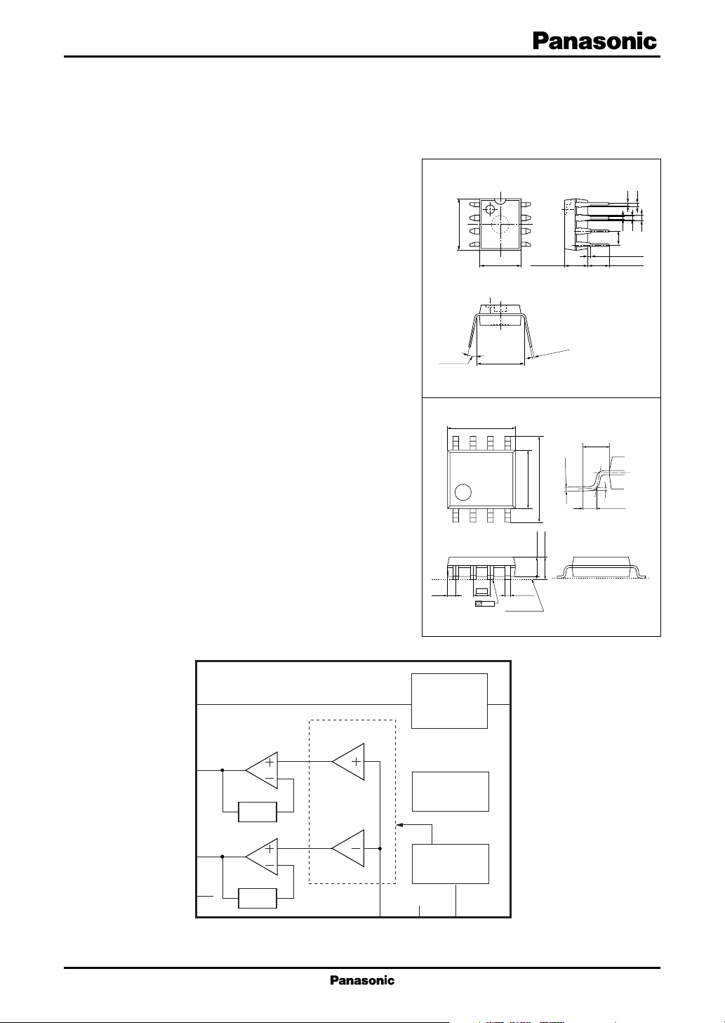
AN7511
1
2
3
9.2±0.2
4
5.01±0.20
6.4±0.2
7.62±0.303° to 15°
DIP008-P-0300
58
41
Unit: mm
8
7
6
5
3.35±0.20 3.89±0.20
+0.10
–0.05
0.30
2.54
0.30±0.26
Unit: mm AN7511S
(1.05)
0.15±0.10
6.40±0.20
4.30±0.20
1.45±0.10
1.75max.
0° to10°
0.50±0.20
0.9
1.0
0.5
1.3
1.5
■ Block Diagram
Output
Output
(for output)
V
CC
GND
(0.60)
1.27
+0.10
0.40
–0.05
0.10
Seating plane
SOP008-P-0225C
5
Ripple
rejection
1
Standby
circuit
Attenuator
6
Thermal
shutdown
28 dB
8
Attenuator
control
7
28 dB
2
Input
3
GND
4
Mute
1
AN7511, AN7511S ICs for Audio Common Use
■ Pin Descriptions
Pin No. Description
1 Standby (standby state if this pin is open.)
2 Input
3 Ground (for input)
4 Muting (muting on if this pin is open.)
5 Supply voltage
6 + Output
7 Ground (for output ch.1)
8 − Output
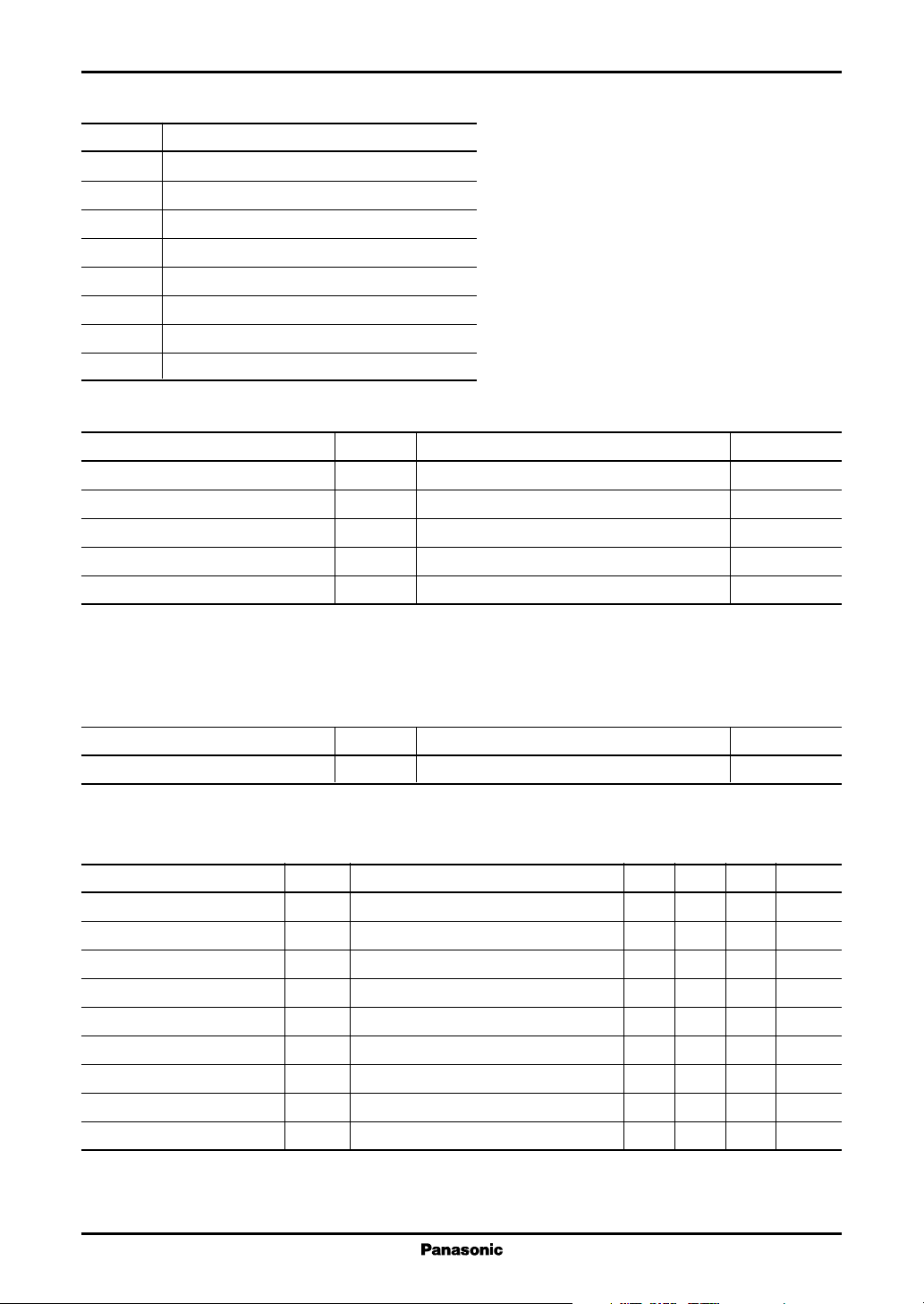
■ Absolute Maximum Ratings
Parameter Symbol Rating Unit
2
Supply voltage
Supply current I
Power dissipation
Operating ambient temperature
Storage temperature
Note)*1: Except for the operating ambient temperature and storage temperature, all ratings are for Ta = 25°C.
2: At no signal
*
3: The power dissipation shown is the value for Ta = 70°C.
*
*
3
*
1
*
1
*
V
CC
CC
P
D
T
opr
T
stg
14 V
1.0 A
541 mW
−25 to +70 °C
−55 to +150 °C
■ Recommended Operating Range
Parameter Symbol Range Unit
Supply voltage V
CC
3.5 to 13.5 V
■ Electrical Characteristics at VCC = 5.0 V, RL = 8 Ω, f = 1 kHz, Ta = 25°C ± 2°C
Parameter Symbol Conditions Min Typ Max Unit
Quiescent circuit current I
Standby current I
Output noise voltage
*
V
Voltage gain G
Total harmonic distortion THD PO = 0.25 W 0.05 0.5 %
Maximum output power P
Ripple rejection ratio
*
RR Rg = 10 kΩ, VR = 1 V[rms], fR = 120 Hz 30 50 dB
Output offset voltage V
Muting effect
Note)*: In measuring, the filter for the range of 15 Hz to 30 kHz (12 dB/OCT) is used.
*
MT PO = 0.25 W 70 86 dB
VIN = 0 mV 30 60 mA
CQ
VIN = 0 mV 110µA
STB
Rg = 10 kΩ0.14 0.4 mV[rms]
NO
PO = 0.25 W 32 34 36 dB
V
THD = 10% 0.8 1.1 W
O1
Rg = 10 kΩ−300 0 300 mV
OFF
2
ICs for Audio Common Use AN7511, AN7511S
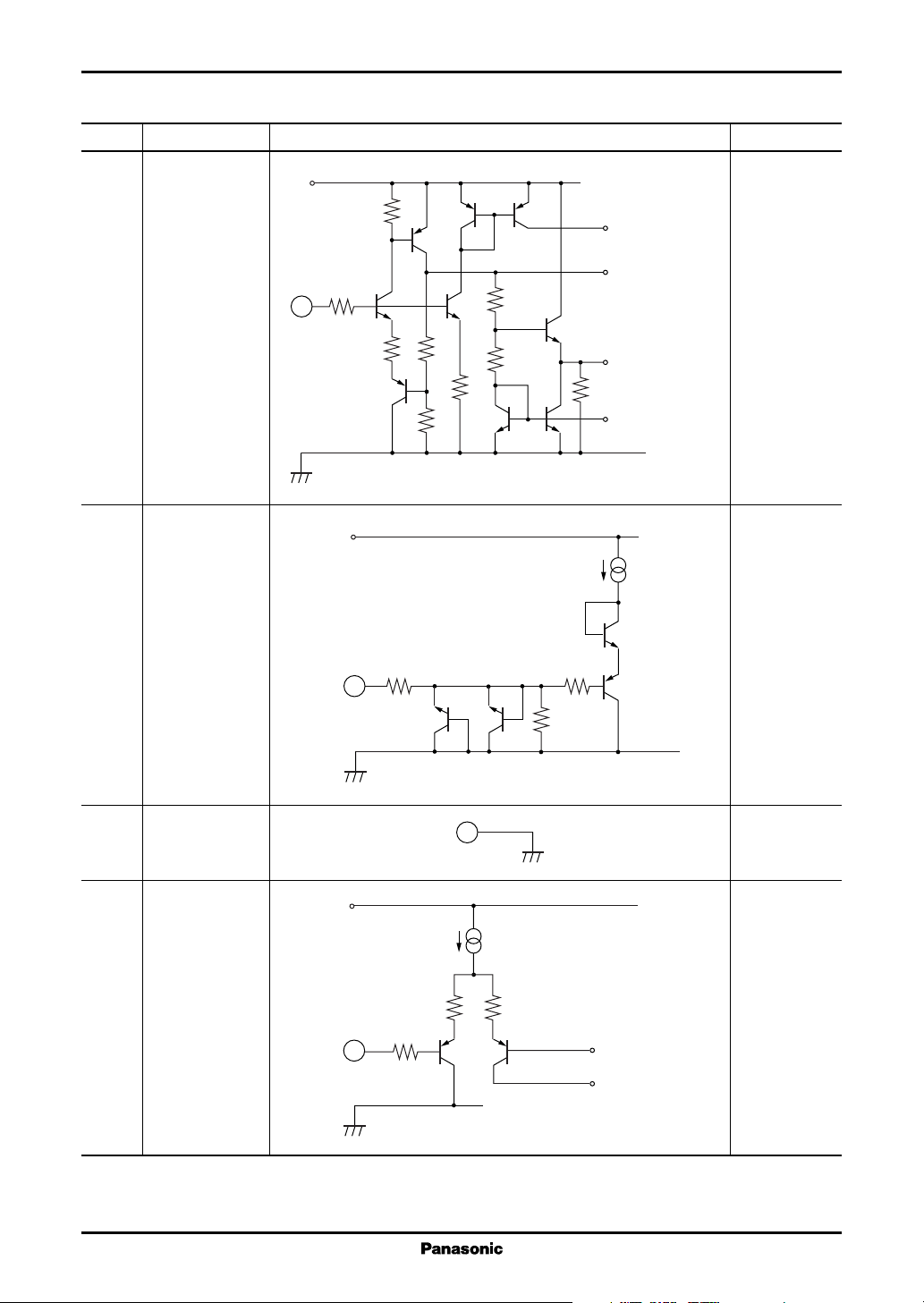
■ Terminal Equivalent Circuits
Pin No. Pin name Equivalent circuit Voltage
1 Standby pin 5 V
V
CC
30 kΩ
To the shock
sound prevention
circuit
V
RF
(≈ VCC)
1
200 Ω
2 kΩ
50 kΩ
12 kΩ 10 kΩ
33 kΩ
5 kΩ
1/2 V
CC
10 kΩ
To the constant
current circuit
2 Input pin 0 mV to 10 mV
V
CC
30 µA
200 Ω 400 Ω
2
30 kΩ
3 GND 0 V
4 Muting pin
V
CC
3
50 µA
5 kΩ
5 kΩ
200 Ω
4
Ref. = 1.25 V
To Mute
3
 Loading...