

Panasonic AN7397S, AN7397K Datasheet
ICs for Audio Common Use
AN7397K, AN7397S
Spatializer IC for I2C bus
■ Overview
Spatializer Audio Processor is a signal processing technology, monopolized by Desper Products,
Inc., that was developed for commercial electronics
and multimedia markets, and is based on Desper's
“PRO Spatializer” that is a 3-D audio production
system for business use. The AN7397K, AN7397S
utilizes the innovative technology adopted in that
system, and provides sound enhancement effect and
sound expansion with the conventional 2-speaker stereo system.
■ Features
• Provides deep 3-D sound with conventional 2speaker system.
• The audio signal recorded through this IC can be
reproduced with usual stereo system.
• Performs optimal processing to the sound source
recorded with surround-effect so as not to give
double effects.
• Sound localization can be varied.
• A pseudo stereo effect for the monaural audio sig-
nal is achieved.
• Positions and moves each sound source on 270°
arc in real time.
• An on-chip serial control bus (i.e., I
space-effect and change modes.
2
C) to vary
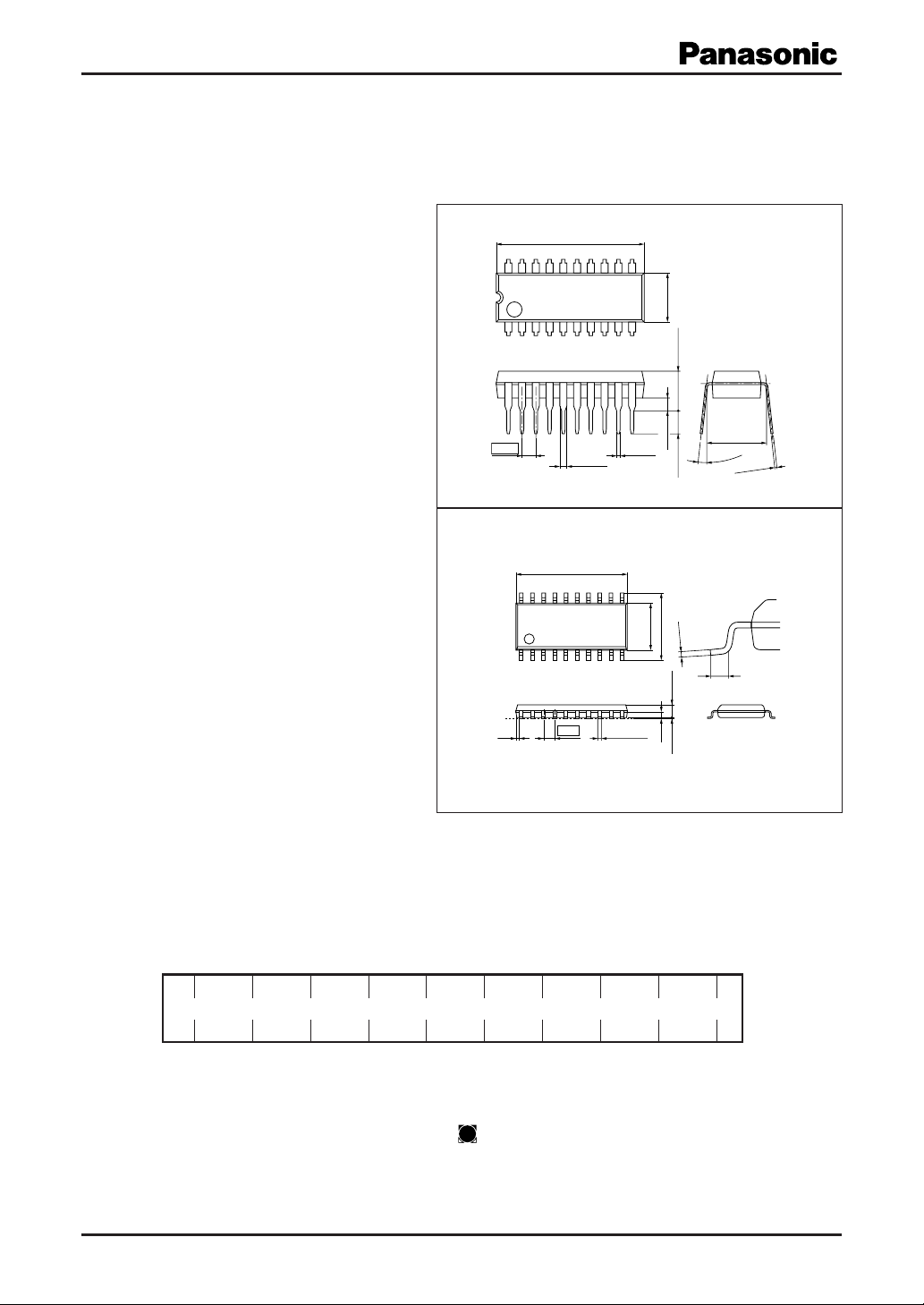
AN7397K
19.1±0.3
20 11
110
1.778
0.9±0.25
0.5±0.1
SDIP020-P-0300
AN7397S
12.6±0.3
20 11
5.4±0.3
110
0.4 0.40±0.25
1.27
SOP020-P-0300B
6.35±0.30
4.50±0.253.45±0.25
1.1±0.25
7.7±0.3
0.15
0.65
0.1±0.1 1.5±0.2
7.62±0.25
3° to 15
0.35
0.3
Unit: mm
°
+0.1
– 0.05
Unit: mm
■ Applications
• Televisions, videos, audio equipment, DVDs, personal computers, and game machines
Note) The packages (SDIP020-P-0300 and SOP020-P-0300B) of this
product will be changed to lead-free type (SDIP020-P-0300A
and SOP020-P-0300E). See the new package dimensions sec-
tion later of this datasheet.
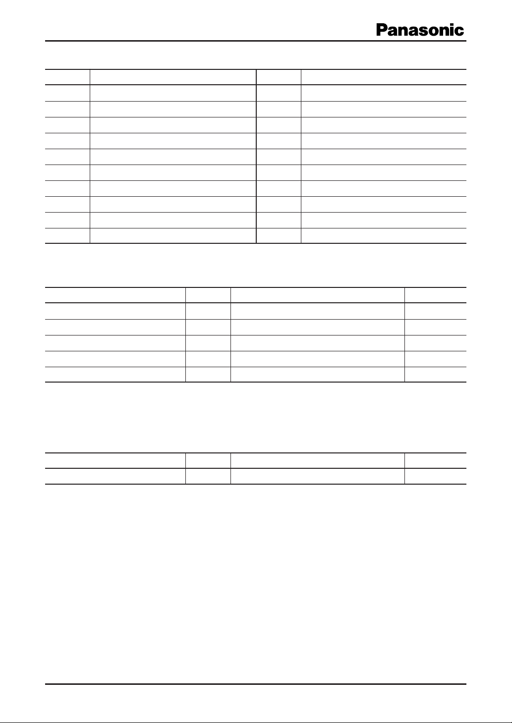
■ Pin Assignment
14
7
CC
V
Mode
R-det.2
13
8
L-ret.
R-det.1
12
9
D-GND
SDA
11
10
SCL
GND
20
1
L-in
19
2
R-in
CC
1/2 V
18
3
F-out
L-out
17
4
F-in
S-out
16
5
VCA
R-out
Space
15
6
R-ret.
Note) Spatializer and the device trademark of circle-in-square are owned by Desper Products Inc.
This product can be used with the consent of the Desper Products Inc.
Under the terms of the agreement between Matsushita Electric and Desper Products Inc., no technical information on the
Spatializer, which is applied to this product, shall be provided.
Publication date: October 2002 SDC00027BEB
1
AN7397K, AN7397S
■ Pin Descriptions
Pin No. Description
1 L-in
2 1/2 V
CC
3 L-out
4 S-out
5 R-out
6 R-ret.
7 Mode
8 L-ret.
9 D-GND
10 SCL
■ Absolute Maximum Ratings
Parameter Symbol Rating Unit
Supply voltage V
Supply current I
2
Power dissipation
Operating ambient temperature
Storage temperature
Note)*1: Except for the operating ambient temperature and storage temperature, all ratings are for Ta = 25°C.
2: The power dissipation shown is the value for Ta = 75°C
*
*
1
*
1
*
CC
CC
P
D
T
opr
T
stg
Pin No. Description
11 SDA
12 R-det.1
13 R-det.2
14 V
CC
15 Space
16 VCA
17 F-in
18 F-out
19 R-in
20 GND
7.0 V
100 mA
230 mW
−25 to +75 °C
−55 to +125 °C
■ Recommended Operating Range
Parameter Symbol Range Unit
Supply voltage V
2
CC
4.5 to 6.8 V
SDC00027BEB
■ Electrical Characteristics at VCC = 5 V, f = 1 kHz, Ta = 25°C ± 2°C
Parameter Symbol Conditions Min Typ Max Unit
Total circuit current I
3
Maximum output voltage
Output noise voltage 1
3
Voltage gain 1
*
Total harmonic distortion 1
Output noise voltage 2
6
Voltage gain 2
*
Total harmonic distortion 2
*
1, 4
*
*
1, 5
*
*
TOTALVIN
V
OUT1
V
NO1
G
V1
2, 3
THD1L-out, R-out VIN = 400 mV 0.05 0.2 %
V
NO2
G
V2
2, 6
THD2S-out VIN = 60 mV 0.15 0.3 %
I2C interface
Sink current at ACK I
SCL/SDA signal input high- level V
SCL/SDA signal input low- level V
Input-enable maximum frequency f
Note) *1: In measuring, the filter with A-characteristic curve is used.
*2: In measuring, the filter for the range of 15 Hz to 30 kHz (12 dB/OCT) is used.
*3: Mode: ST, L-in + R-in, VCA (I2C data: BFH)
*4: Mode: ST, VCA (I2C data: BFH)
*5: Mode: ST, VCA (I2C data: 80 H)
*6: Mode: ST, VCA (I2C data: 80 H) for either L-in or R-in
ACK
IHI
ILO
Imax
= 0 mV 18 25 32 mA
L-in, R-in THD = 1% 0.8 1.0 V[rms]
L-out, R-out RG = 4.7 kΩ20 50 µV[rms]
L-out, R-out VIN = 400 mV −20 2 dB
S-out RG = 4.7 kΩ80 200 µV[rms]
S-out VIN = 60 mV 343 450 685 mV[rms]
Maximum value of sink current of 2.0 10 mA
pin 11 at ACK
AN7397K, AN7397S
2.5 3.5 V
0 0.5 V
100 Kbit/s
• Design reference data
Parameter Symbol Conditions Min Typ Max Unit
I2C interface
Bus free before start t
Start condition set-up time t
Start condition hold time t
SCL/SDA low period t
SCL high period t
SCL/SDA rise time t
SCL/SDA fall time t
Data set-up time (Write) t
Data hold time (Write) t
Acknowledge set-up time t
Acknowledge hold time t
Stop condition set-up time t
DAC
6-bit DAC DNLE L
BUF
SU, STA
HD, STA
LO
HI
R
F
SU, DAT
HD, DAT
SU, ACK
HD, ACK
SU, STO
6
1 LSB = (Data (max.) − Data (00))/63
4.0 µs
4.0 µs
4.0 µs
4.0 µs
4.0 µs
1.0 µs
0.35 µs
0.25 µs
0 µs
3.5 µs
0 µs
4.0 µs
0.1 1.0 1.9 LSB
step
SDC00027BEB
3
 Loading...