

Panasonic AN7374K Datasheet
■ Overview
The AN7374K, AN7376S are 2-ch dolby B/C type noise
reduction ICs. Filter circuits (MPX filter driver and spectral
skewing, etc.) are incorporated in 28-pin package. It can
configure with very few external parts.
■ Features
•
Fewer external parts
•
Spectral skewing circuit and anti-saturation circuit built-
in.
•
Available for double deck (Through signal output to
REC output at PB mode.)
•
Available for ±2 or 1 power supply
*
Dolby is the trademark of Dolby Laboratories Licensing
Cor-poration.
ICs for Cassette, Cassette Deck
AN7374K, AN7376S
Dolby* B/C Type Noise Reduction IC
28 27 26 25 24 23 22 21 20 19 18 17 16 15
1 2 3 4 5 6 7 8 9 10 11 12 13 14
V
CC
GND
++
++
Buff.
Buff.
Bias
Switch
Logic
Mpx–Dr
Mpx–Dr
V
REF
Stab
SS
SS
Line
Line
VCR–H
Rect–H
Rect–H
OS–H
OS–H
AS
AS
VCR–L
V
REFIREF
VCR–H VCR–L
Rect–L
Rect–L
OS–L
OS–L
■ Block Diagram
1
2
3
4
5
6
7
8
9
10
11
12
13
14 15
16
17
18
19
20
21
22
23
24
25
26
27
28
0.4±0.25 0.451.27
0.1±0.1
0.3
9.4±0.3
0.15
0.925
2.0±0.2
17.81±0.3
Unit : mm
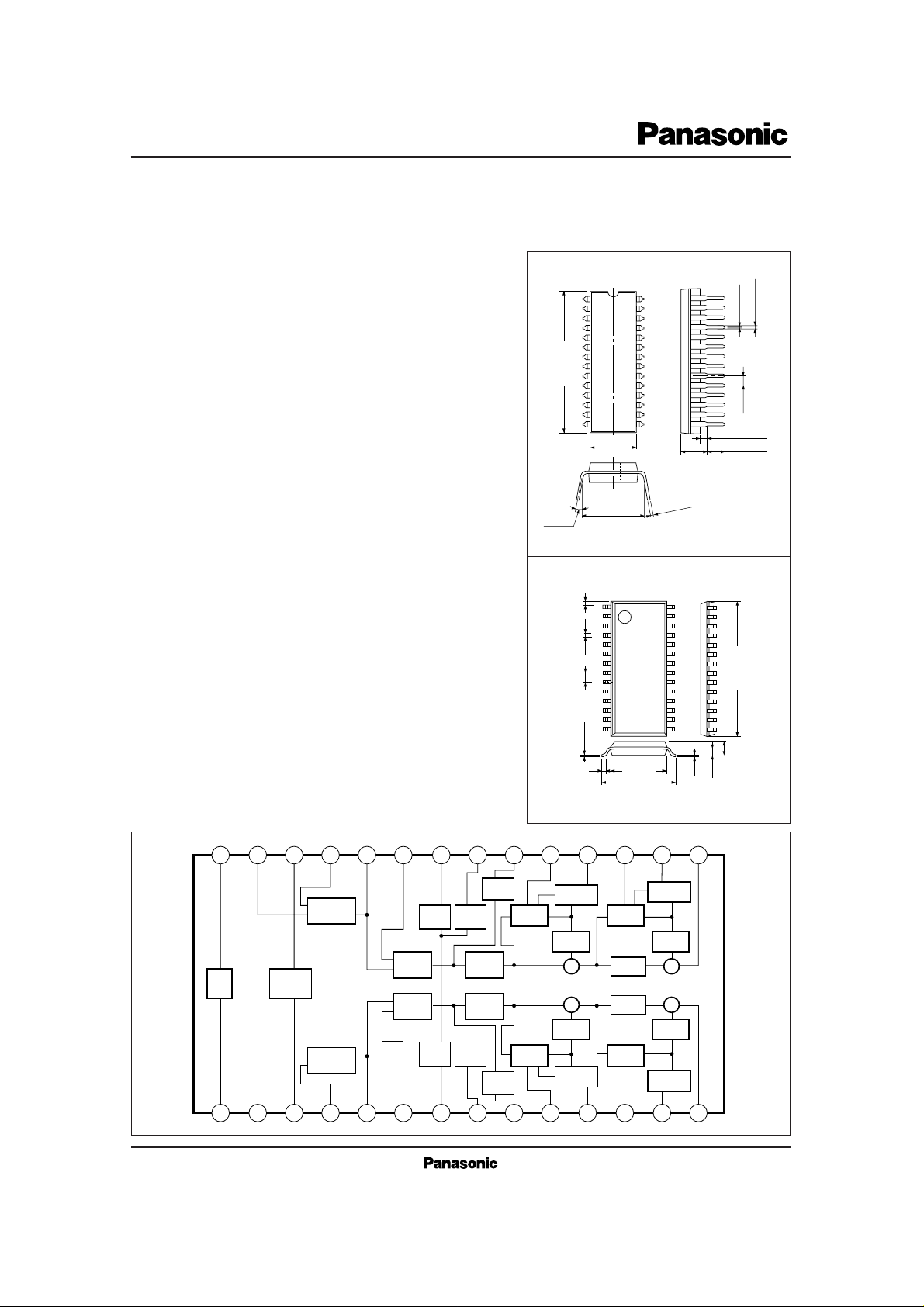
AN7376S
7.2±0.3
28-Lead SOP Package (SOP028-P-0375A)
AN7374K
1
2
3
4
5
6
7
8
9
26.7±0.3
10
11
12
13
14
8.4±0.3
3 ~15˚
10.16±0.25
28-Lead Shrunk DIP Package (SDIP028-P-0400A)
28
27
26
25
24
23
22
21
20
19
18
17
16
15
4.8±0.25
+ 0.1
– 0.05
0.3
Unit : mm
±0.1
0.9±0.25
0.5
1.778
1.05±0.25
3.05±0.25
ICs for Cassette, Cassette Deck
AN7374K, AN7376S
■ Absolute Maximum Ratings (Ta=25˚C)
13.5
22
300
–30 ~ + 80
–55 ~ + 150
V
CC
I
CC
P
D
T
opr
T
stg
Supply Voltage
Supply Current
Power Dissipation
Operating Ambient Temperature
Storage Temperature
V
mA
mW
˚C
˚C
Parameter Symbol Rating Unit
■ Recommended Operating Range (Ta= 25˚C)
Parameter Symbol Range
Operating Supply
Voltage Range
V
CC
9V ~ 13V or ± 4.5V ~ ±6.5V
7V ~ 13V or ± 3.5V ~ ±6.5V
AN7374K
AN7376S
Parameter Symbol min. typ. max. Unit
■ Electrical Characteristics
(Ta
=25˚C
, V
CC
=
12V, In the Dolby Reference Level ; 388mVrms (
= –
6dBm) REC – OUT)
Quiescent Current
12I
CQ
19 mA15
R/P
NR f(Hz) Others
R off
No signal
Rec.– IN to Rec.– OUT Gain
17Grin 21 dB19R off 1k V
in
= 0dB
PB – IN to Rec.– OUT Gain
22Gpin 26 dB24P off 1k V
in
= 0dB
DGmpx – 1 0 1 dBMPX ON/OFF Gain Difference
P →
Pm
off 1k Vin = 0dB
V
lout
LINE – OUT
Output Level
AN7374K
AN7376S
P off 1k V
in
= 0dB
500
330
580
388
670
450
mVrms
mVrms
9.4B – R – 1 11.9 dB10.4R B 10k Vin = – 40dB
B Type
Encode · Boost
6.7B – R – 2 9.7 dB8.2R B 5k V
in
= – 30dB
4.2B – R – 3 7.2 dB5.7R B 1k Vin = – 25dB
– 1.1B – R – 4 1.9 dB0.4R B 10k Vin = 0dB
1
2
3
4
18.1C – R – 1 21.6 dB19.6R C 1k Vin = – 60dB
C Type
Encode · Boost
11.5C – R – 2 15.5 dB13.5R C 5k V
in
= – 40dB
8.7C – R – 3 12.7 dB10.7R C 300 Vin = – 30dB
3.5C – R – 4 7.5 dB5.5R C 5k Vin = – 25dB
1
2
3
4
– 8.3C – R – 5 – 4.3 dB – 6.3R C 15k Vin = 0dB5
V
Omax.
AN7374K
AN7376S
R off 1k
12
12
14
14
dB
dB
THD
= 1%
VCC = 9.0V
VCC = 7.0V
THD
off
0.15 %0.02R off 1k Vin = 0dB
Distortion
THD – C 0.3 %0.13R C 1k V
in
= 0dB
off
C
S/N 60.0 62.5 dBSN Ratio
R
g
= 5.1kΩ
CCIR/ARM
R C
CT – R – P dB – 80P off 1k Vin = 0dB
CT – P – R dB – 80R off 1k Vin = 0dBCrosstalk
CT – C – C dB – 80R off 1k Vin = 0dB
Rec.→PB
PB→Rec.
Ch.→Ch.
V
off
– 70 0 70 mVMode Switching Offset R
off
→C
No signal
Channel Balance
– 1.0D – G
V
1.0 dB0R off 1k Vin = 0dB
9.0VC – P 12.5 V
5.0VC – R 7.0 V
Mode Control
Voltage
– 0.5VC – Pm 3.0 V
PB
Rec.
PBmpx
9.0VC – C 12.5 V
5.0VC – B 7.0 V
Pin3
Applied Voltage
NR Control Voltage
– 0.5VC – off 3.0 V
C
B
off
Condition
Signal · Handling
Pin26
Applied Voltage
ICs for Cassette, Cassette Deck
AN7374K, AN7376S
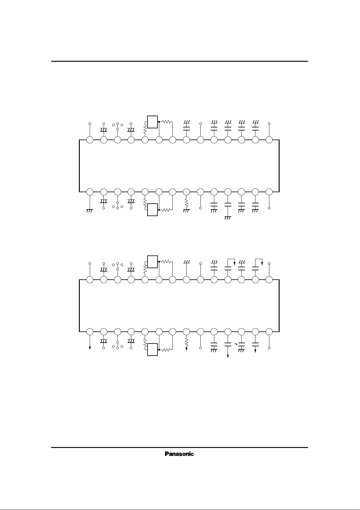
■ Application Circuits
28 27 26 25 24 23 22 21 20 19 18 17 16 15
1 2 3 4 5 6 7 8 9 10 11 12 13 14
+ +
+ +
AN7374K
28 27 26 25 24 23 22 21 20 19 18 17 16 15
1 2 3 4 5 6 7 8 9 10 11 12 13 14
+ +
+ +
AN7374K
+V
CC
1µF
Rec. In
PB/Rec.
/PBmpx
1µF
PB In
MPX
FIL
2.4kΩ
5.6kΩ
1µF
Line Out
1500pF 1500pF 0.47µF
0.47µF
Rec. Out
GND
Rec. In off/B/C PB In
MPX
FIL
2.4kΩ
5.6kΩ
Line Out
1500pF 1500pF 0.47µF
0.47µF
Rec. Out
1µF 1µF
22kΩ
+V
CC
1µF
PB/Rec.
/PBmpx
1µF
PB In
MPX
FIL
2.4kΩ
5.6kΩ
Line Out
1500pF 1500pF
0.47µF
0.47µF
Rec. OutRec. In
GND
–V
CC
1µF
Rec. In off/B/C PB In
2.4kΩ
MPX
FIL
5.6kΩ
22kΩ
Line Out Rec. Out
1500pF 1500pF
0.47µF
1µF
0.47µF
• For 1 Power Supply
• For ±2 Power Supply
Note) When users use this product, licensing contract should be made between the Dolby Research Center.
Details should be contacted with the following.
Dolby Research Center. Tokyo Office (Far Eastan Continental Inc.)
TEL : 03-3584-0039
 Loading...