

Panasonic AN7354SC Datasheet
ICs for Cassette, Cassette Deck
■ Overview
The AN7354SC is an IC for 2 ch. Dolby B/C-Type noise
reduction process. It requires fewer external parts and
incorporates the functions of line-output muting and level
detection and the delay circuit.
■ Features
•
Built-in spectral skewing circuit not requiring external
parts
•
Line-output muting circuit built-in
•
PB input delay circuit built-in
•
Built-in level detection circuit for automatic level adjust-
ment and level meter
•
ON/OFF of NR, B-/C-type, REC./PB, MPX and muting
function, and Hi/Lo changeover of level detection gain,
directly-controllable by microcomputer
*
Dolby symbols are the trademarks of Dolby Laboratory
Licensing Corporation. The use of this products
requires the approval of Dolby Laboratories Licensing
Corporation in advance.
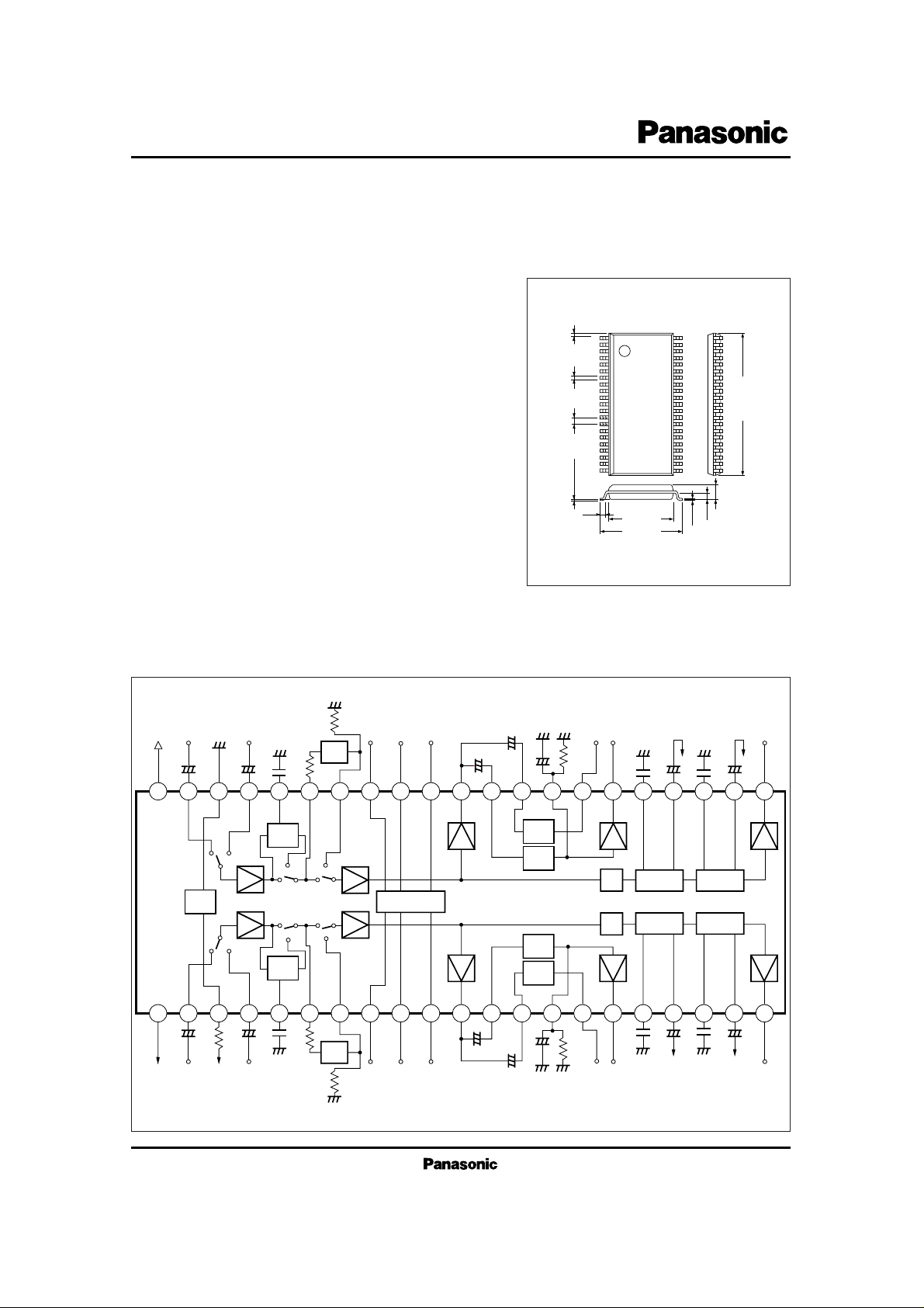
AN7354SC
Dolby* B/C-type Noise Reduction
0.45
0.35±0.1
1.0
0.1±0.1
0.3
2.0±0.2
0.9
0.15
1
9.5±0.3
11.5±0.3
Unit : mm
21.25±0.3
42
21 22
42-Lead SSOP Package (SSOP042-P-0450)
■ Block Diagram
V
CC
REC.
IN
Bias
LOGIC
REC.
/PB
MPX
OFF/
ON
LINE
OUT
LEVEL
METER
OUT
REC. OUT
METER
0dB
/20dB
PB
IN
1500pF
5.6kΩ
1µF1µF
100kΩ
1500pF 1500pF
2.4kΩ
42 2241 40 39 38 37 36 35 34 33 32 31 30 29 28 27 26 25 24 23
1 212 3 4 5 6 7 8 9 10 11 12 13 14 15 16 17 18 19 20
++
++
+
+
+
+
+
+
++
++
2.2µF
0.1µF
1µF
0.47µF
0.47µF
V
EE
REC.
IN
NR
ON/
OFF
C/B
-type
LINE
OUT
LEVEL
METER
OUT
REC. OUT
Mute
ON/OFF
PB
IN
1500pF
5.6kΩ
2.4kΩ
22kΩ
100kΩ
1500pF
1500pF
2.2µF
0.1µF
1µF1µF
1µF
0.47µF
0.47µF
Delay
Delay
Mute
HLS
HLS
LLS
LLS
Rect
Rect
MPX
MPX
SS
SS
Mute
ICs for Cassette, Cassette Deck
AN7354SC
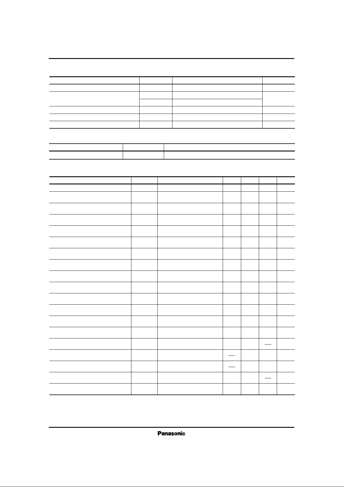
■ Absolute Maximum Ratings (Ta=25˚C)
V
CC
ICC (+)
I
CC
(–)
P
D
T
opr
T
stg
Supply Voltage
Supply Current (Ta=75˚C)
Power Dissipation (Ta=75˚C)
Operating Ambient Temperature
Storage Temperature
V
mA
mW
˚C
˚C
Parameter Symbol Rating Unit
±6.7
+22
–22
295
–20 ~ + 75
–55 ~ + 125
Parameter Symbol Range
■ Recommended Operating Range (Ta=25˚C)
Operating Supply Voltage Range
V
CC
±4.5V ~ ±6.5V
■ Electrical Characteristics (VCC= ± 6V, Ta=25˚C ± 2˚C)
Parameter Symbol Condition min. typ. max. Unit
Total Circuit Current
Note 1)
12I
CC
20 mA16
REC., OFF, No input signals
G
rin
17 19 21 dB
REC., OFF, f = 1kHz
REC. – OUT Level 388mV
REC. – IN to REC. – OUT
I/O Gain
Note 2)
G
pin
22 24 26 dB
PB, OFF, f = 1kHz
REC. – OUT Level 388mV
PB – IN to REC. – OUT
I/O Gain
Note 3)
DG
mpx
– 1 0 1 dB
PB, OFF, f = 1kHz
Gain difference from Gpin
MPX ON/OFF Gain Difference
V
lout
510 570 640 mVrms
PB, OFF, f = 1kHz
V
in
= 0dB
LINE – OUT Level
BR – 1 9.4 10.4 11.9 dB
REC., B, f = 10kHz
V
in
= – 40dB
B-type Encode Boost (1)
BR – 2 6.7 8.2 9.7 dB
REC., B, f = 5kHz
V
in
= – 30dB
B-type Encode Boost (2)
BR – 3 4.2 5.7 7.2 dB
REC., B, f = 1kHz
V
in
= – 25dB
B-type Encode Boost (3)
BR – 4 – 1.1 0.4 1.9 dB
REC., B, f = 10kHz
V
in
= 0dB
B-type Encode Boost (4)
CR – 1 18.1 19.6 21.6 dB
REC., C, f = 1kHz
V
in
= – 60dB
C-type Encode Boost (1)
CR – 2 11.5 13.5 15.5 dB
REC., C, f = 5kHz
V
in
= – 40dB
C-type Encode Boost (2)
CR – 3 8.7 10.7 12.7 dB
REC., C, f = 300Hz
V
in
= – 30dB
C-type Encode Boost (3)
CR – 4 3.5 5.5 7.5 dB
REC., C, f = 5kHz
V
in
= – 25dB
C-type Encode Boost (4)
CR – 5 – 8.3 – 6.3 – 4.3 dB
REC., C, f = 15kHz
V
in
= 0dB
C-type Encode Boost (5)
V
Omax.
12 13 dB
REC., OFF, f = 1kHz
V
CC
= ±4.5V THD = 1%
Signal Handling
THDO 0.02 0.15 %
REC., OFF, f = 1kHz
V
in
= 0dB
Total Harmonics Distortion – off
THDC 0.13 0.3 %
REC., C, f = 1kHz
V
in
= 0dB
Total Harmonics Distortion – C
S/N 60.0 62.5 dB
REC., C, R
g
= 5.1kΩ
CCIR/ARM Weighted
Signal to Noise Ratio
Vofs – R –70 0 70 mV
REC., OFF, → C switch,
REC.
–
OUT potential fluctuation
Mode Switch Offset
Note 1) REC., OFF in the condition description, expresses that MODE is REC. and NR is OFF. The same for the following.
Note 2) Obtain the input voltage of REC. – IN when the output voltage of REC. – OUT becomes 388mVrms. For this input
voltage, the reference level in REC. is assumed 0dB.
Note 3) Obtain the input voltage of PB. – IN when the output voltage of REC. – OUT becomes 388mVrms. For this input voltage,
the reference level in PB is assumed 0dB.
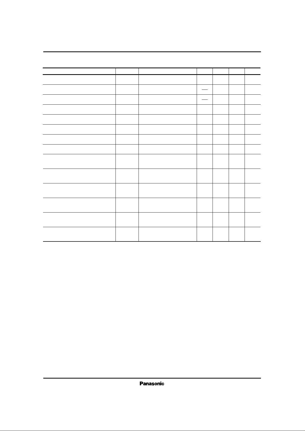
ICs for Cassette, Cassette Deck
AN7354SC
Parameter Symbol Condition min. typ. max. Unit
VPS (1) 2 3 4 VDelay Output (1)
V
in
= – 0.2V
S30 → C PB MPX off
Piny and Pin#7 DC Potential
VPS (2) 4 6 8 VDelay Output (2)
V
in
= + 0.2V
S30 → C PB MPX off
Difference from VPS (1)
VPS (3) – 0.1 0 0.1 VDelay Output (3)
V
in
= – 0.2V
S30 → B PB MPX off
Piny and Pin#7 DC Potential
VPS (4) – 0.2 0 0.2 VDelay Output (4)
V
in
= + 0.2V
S30 → B PB MPX off
Difference from VPS (3)
VPS (5) – 4 –3 –2 VDelay Output (5)
V
in
= – 0.2V
S30 → A PB MPX off
Piny and Pin#7 DC Potential
VPS (6) 4 6 8 VDelay Output (6)
V
in
= + 0.2V
S30 → A PB MPX off
Difference from VPS (5)
CB –1 0 1 dB
Gain difference between
channels, Grin and Gpin
Channel Balance
THDP 0.02 0.15 %
PB, OFF, f = 1kHz
V
in
= 0dB, LINE – OUT
Total Harmonics Distortion Line Out
G
mut
–85 –75 dB
PB, OFF, Mute ON
f = 1kHz, V
in
= 0dB
Line Mute Attenuation
Vofs – M –20 0 20 mV
Mute OFF → ON switching,
LINE – OUT potential fluctuation
Line Mute Offset
VDC (1) 0.9 1.0 1.1 V
PB, OFF, LMG Normal
f = 1kHz, V
in
= – 3dB
Level Meter Output (1)
Note 4)
VDC (2) 3.6 4.0 4.4 V
PB, OFF, LMG Normal
f = 1kHz, V
in
= +9dB
Level Meter Output (2)
VDC (3) 0.9 1.0 1.1 V
PB, OFF, LMG High
f = 1kHz, V
in
= –18dB
Level Meter Output (3)
Vofs – L –15 0 15 mV
PB, OFF, LMG Normal
No Input
Level Meter Output Offset
Note 4) LMG in the condition description is an abbreviation of Level Meter Gain.
■ Electrical Characteristics (Cont.) (VCC= ± 6V, Ta=25˚C ± 2˚C)
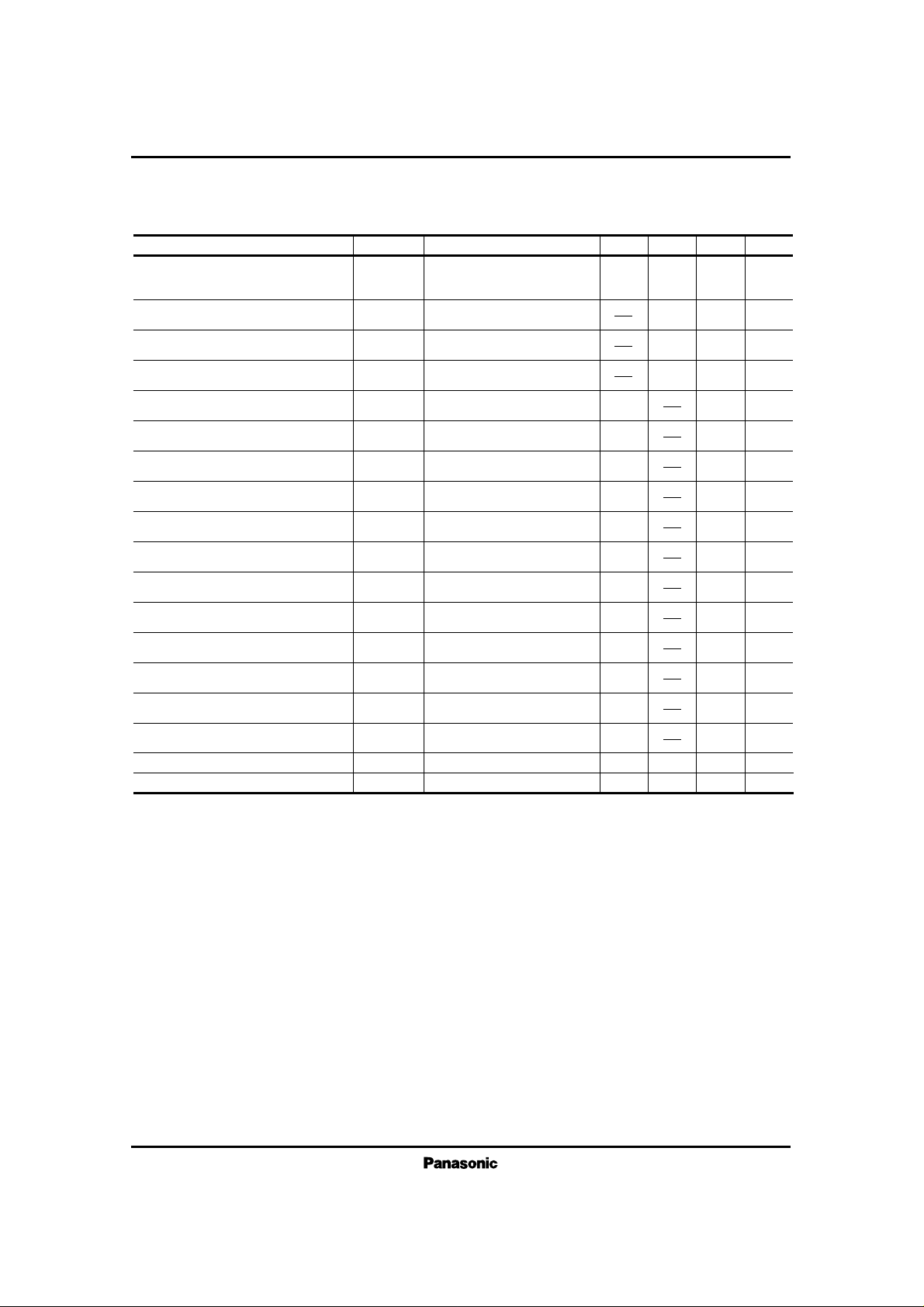
ICs for Cassette, Cassette Deck
AN7354SC
Parameter Symbol Condition min. typ. max. Unit
■ Electrical Characteristics (Ta=25˚C±2˚C) [Design Reference Values]
The following characteristic values are reference values for design but not guaranteed values.
REC.– IN Input Resistance
56.4Rin – RI 75.6 kΩ64
PB – IN Input Resistance
28.05Rin – PI 37.95 kΩ33
V
mut (1)
4.4 6.4 8.4 VDecreased Voltage Mute (1)
PB, OFF, Mute OFF, f=1kHz,
V
in
= 0dB Voltage between
Pins1 and 42 when mute functions
CT– RP –80 –70 dB
PB, OFF, f
= 1kHz
V
in
= 0dB (At REC)
Crosstalk,
REC.– IN to LINE– OUT
CT– CC –80 –70 dB
PB, OFF, f
= 1kHz
V
in
= 0dB
Crosstalk, Cannel to Cannel
VCPB +2.5 +6 V
Pin35 applied DC voltage when
PB, MPX are OFF
PB/REC. Control Voltage PB
VCREC. –1.5 +1.5 VPB/REC. Control Voltage REC.
Pin35 applied DC voltage when
PB, MPX are ON
VCMon –1.5 +1.5 VMPX Control Voltage ON
Pin34 applied DC voltage when
PB, MPX are ON
VCMoff +2.5 +6 VMPX Control Voltage OFF
Pin34 applied DC voltage when
PB, MPX are OFF
VCMnor +2.5 +6 VMeter Control Voltage Normal
Pin33 applied DC voltage when
Meter becomes Normal
VCMhi –1.5 +1.5 VMeter Control Voltage Hi
Pin33 applied DC voltage when
Meter becomes Hi
VCON +2.5 +6 VNR Control Voltage ON
Pin8 applied DC voltage when
NR is ON
VCOFF –1.5 +1.5 VNR Control Voltage OFF
Pin8 applied DC voltage when
NR is OFF
VCC +2.5 +6 VB/C Control Voltage C
Pin9 applied DC voltage for
C-type NR
VCB –1.5 +1.5 VB/C Control Voltage B
Pin9 applied DC voltage for
B-type NR
VCMUon +2.5 +6 VMute Control Voltage ON
Pin10 applied DC voltage when
Mute is ON
VCMUof –1.5 +1.5 VMute Control Voltage OFF
Pin10 applied DC voltage when
Mute is OFF
CT– PR –80 –70 dB
PB, OFF, f
= 1kHz
V
in
= 0dB (At PB)
Crosstalk,
PB– IN to REC.– OUT
 Loading...