

Panasonic AN7353S Datasheet
ICs for Cassette, Cassette Deck
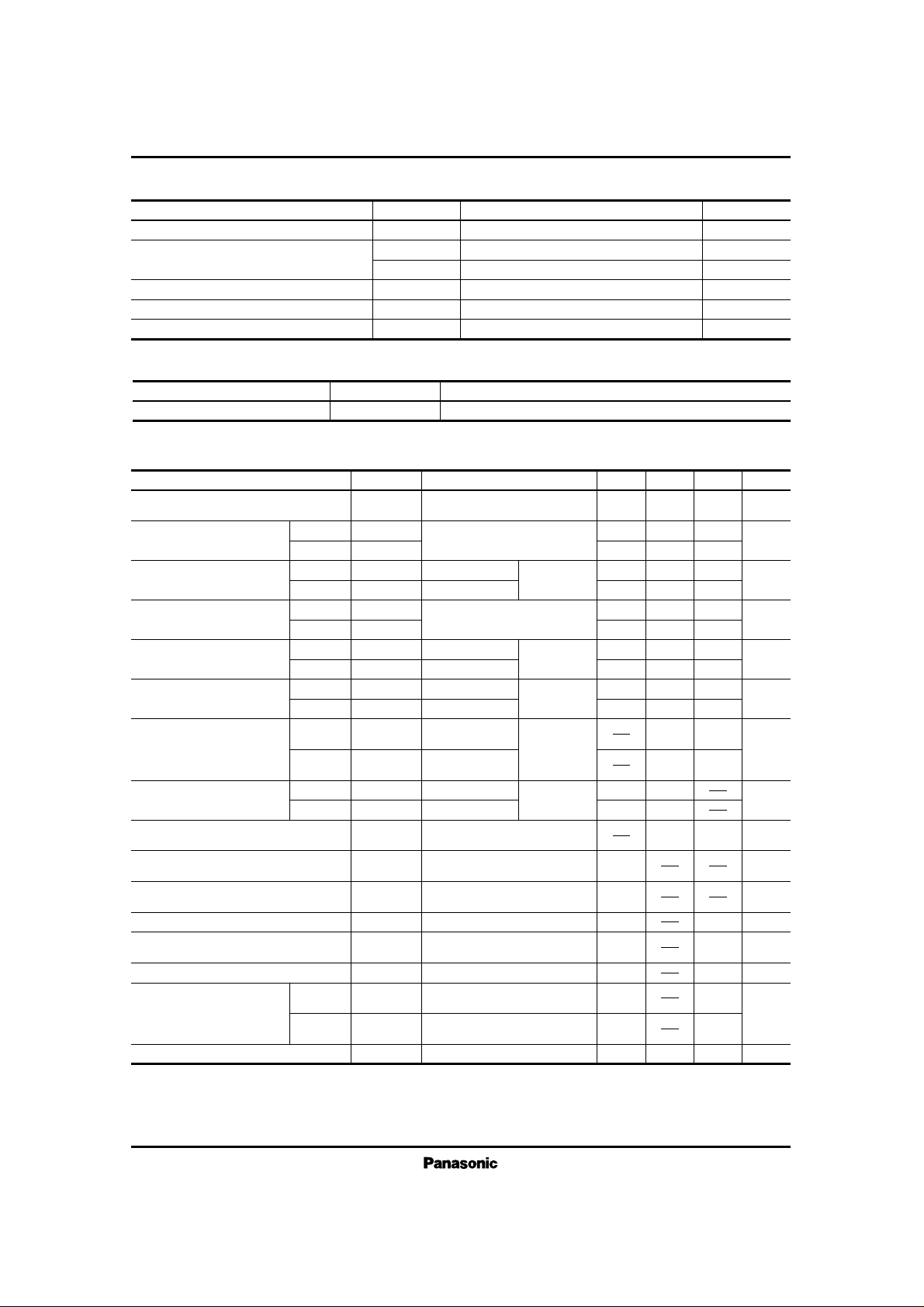
■ Overview
The AN7353S is a bipolar IC developed as a record
equalizer amp. of analogue cassette deck. Particularly in
order to support the automatic adjustment, it incorporates
various volume filter circuits and control functions. Also, it
has realized great reduction of external parts required.
■ Features
•
Fine adjustment of equalizer characteristics (frequency
characteristics and gain) in medium and high frequency
band by DC control
•
Volume for total gain adjustment built-in (±11dB)
•
With pin for low frequency band boost
•
Drive circuit for current output built-in
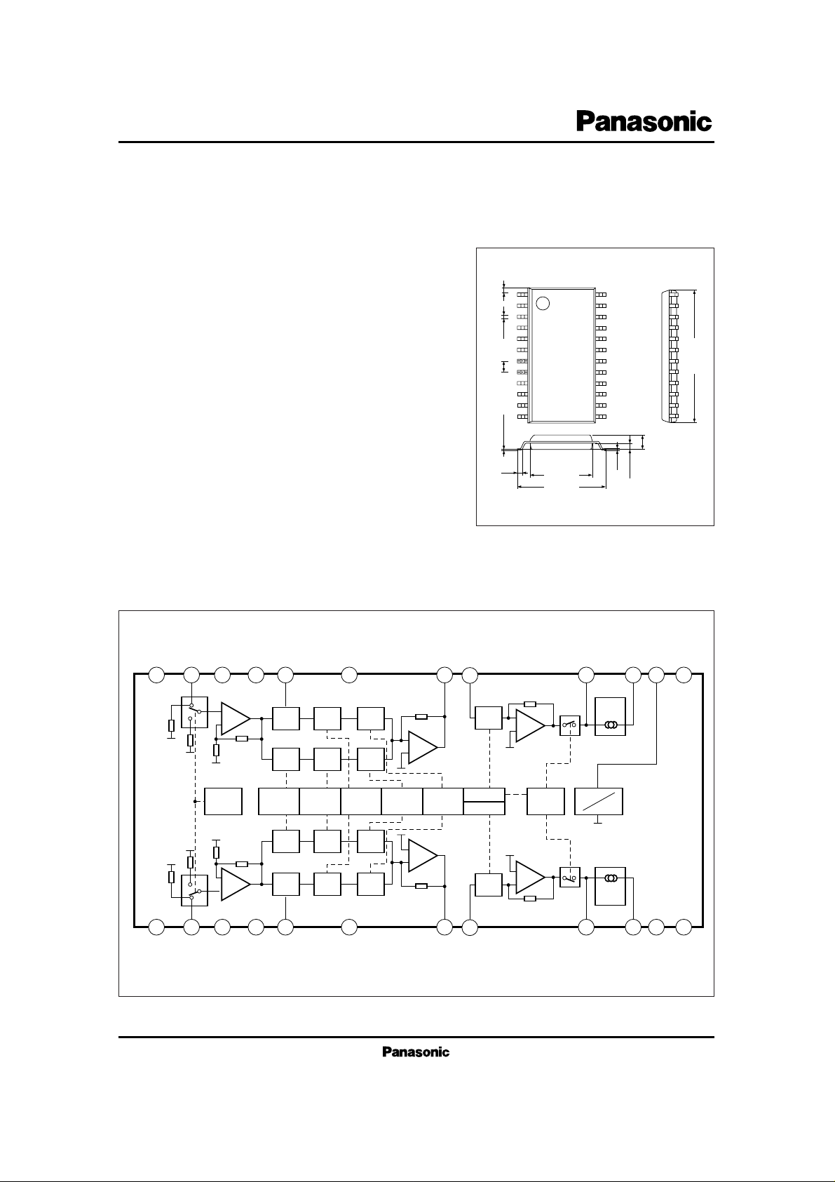
AN7353S
Record Equalizer Amp. for Stereo Cassette Deck
Unit : mm
0.1±0.1
2.0±0.2
0.3
0.925
0.15
0.45
1
2
3
4
5
6
7
8
9
10
11
12
24
23
22
21
20
19
18
17
16
15
14
13
0.4±0.25
1.27
9.4±0.3
7.2±0.3
15.3±0.3
24-Lead SOP Package (SOP024-P-0375)
■ Block Diagram
GND CM
REC.
IN
(L)
CH Boost
(L)
CF
EQ
OUT
(L)
VR
IN
(L)
V
out (L)
I
out (L)
VCCCL
–V
CC
REC.
IN
(R)
IN
MUTE
CQ CP
EQ
OUT
(R)
VRIN
(R)
V
out
(R)
I
out (R)
NC CR
Amp.
Amp.
Amp.
Q
GT (L)
V
REF
Output
Sw.
Ireg –
GT (R)
GHGpfmfp
Amp.
Rec.
Rec.
L.P.F
fm
V– I
GH
V– I
L.P.F
fm
V– I
GH
V– I
GT
V– I
GT
V– I
V– I
Conv.
V– I
Conv.–
Q
V– I
Input
Sw.
fp
V– I
Gp
V– I
Q
V– I
fp
V– I
Gp
V– I
1 2 3 4 5 6 7
8
9 10 11 12
24 23 22 21 20 19 18
17
16 15 14 13
Boost
(R)
ICs for Cassette, Cassette Deck
AN7353S
V
CC
ICC (+)
I
CC
(–)
P
D
T
opr
T
stg
■ Absolute Maximum Ratings (Ta=25˚C)
Supply Voltage
Supply Current
Power Dissipation
Operating Ambient Temperature
Storage Temperature
V
mA
mA
mW
˚C
˚C
Parameter Symbol Rating Unit
±6.7
26
23
521
–25 ~ + 75
–55 ~ + 125
± 4.5V ~ ± 6.5V
■ Recommended Operating Range (Ta= 25˚C)
Parameter Symbol Range
Operating Supply Voltage Range
V
CC
■ Electrical Characteristics (VCC= ±6V, Ta=25±2˚C)
Parameter Symbol Condition min. typ. max. Unit
Reference Output (EQ Output)
– 4 –1.5 +1 dBv
VEQ
f
in
= 400Hz,
V
in
= –6dBv
Medium/High Frequency
Band Gain
GHH
GHL
–900
Voff
(EQ)
mV
Output Offset Voltage (EQ Output)
Rg = 0Ω
+500
f
in
= 10kHz,
V
in
= –12dBv, V
EQ
= 0dB
dB
3.5
–8.5
5.5
–6.5
7.5
– 4.5
HIGH
LOW
High Frequency Band
Peak Gain
GPH
GPL
V
in
= –30dBv
V
in
= –18dBv
dB
16
7
18
9
20
11
f
in
= 25kHz
V
EQ
= 0dB
GQW
GQL
f
in
= 10kHz,
V
in
= –18dBv, V
EQ
= 0dB
dB
2
–2.5
4.5
07+2.5
WIDE
NALLOW
High Frequency Band Peak
Band Width (10kHz Output)
VfPH
VfPL
f
in
= 35kHz
f
in
= 10kHz
V
3.85
1
4.25
1.2
4.65
1.4
HIGH
LOW
V
in
= –30dBv
GTH
GTL
V
in
= –18dBv
V
in
= 0dBv
dB
16.5
–5.5
18.5
–3.5
20.5
–1.5
HIGH
LOW
f
in
= 1kHz
(VR Input)
Volume Amp. Gain
(VOL Output)
V
in
= –14dBv
RL
V
= 10kΩ
V
in
= –14dBv
RL
V
= 1kΩ
Total Harmonics Distortion
VOL
CULL
THD
(RU)
THD
(RC)
f
in
= 1kHz
0.3
0.8
%
0.3
0.8
Maximum Output Voltage
V
O (RU)
V
O (RC)
RLV = 10kΩ
RL
V
= 1kΩ
Vrms
2.2
1
3.2
1.5
VOL
CULL
THD
= 3%
Output Noise Voltage
(CURR Output)
VN
(RC)
0.6 2
mV · rms
Rg = 0Ω
RL
V
= 1kΩ, DIN/AUDIO
Input Muting Attenuation
(EQ Output)
IM
(EQ)
40
dB
f
in
= 1kHz, 3p : OPEN
V
in
= – 6dBv
Output Muting Attenuation
(VOL Output)
OM
(RU)
60 dB
f
in
= 1kHz, V
CL
= 0.3V
V
in (VR)
= 0dBv
Output Offset Current
(CURR Output)
Voff
(RC)
–25
+25
µA
RL
V
= 1kΩ
RL
V
= 100kΩ
–9VPN
(RC)
mV
P–O
Pulse Noise Current (CURR Output)
R
g
= 0Ω
+9
High Frequency Band Peak
Frequency Control Voltage
Pin3 threshold value voltage
(Mute ON voltage)
Pin13 threshold value voltage
(Mute ON voltage)
Muting Control Voltage
Input Side
Output Side
VIM
VOM
3.9
GND
V
CC
V
0.3
20I
tot
mA
Consumption Current No signal
23
26
HIGH
LOW
 Loading...