

Panasonic AN7289NFBQ Datasheet
ICs for FM/AM Tuner
AN7289NFBQ
FM-FE+AM IC for car radio
■ Overview
The AN7289NFBQ is an IC having FM-FE+AM
functions for car radio. A tuner block of car radio can be
constructed by using this IC and the AN7293NSC/NFBQ.
■ Features
• A less number of electrolytic capacitors is required (3
capacitors reduction compared with our conventional
IC)
• AM: Effective sensitivity is improved by 2 dB through
ATC
• AM: Strong-input characteristic is improved by 2-loop-
AGC function
• The AN7289NSC of DIL package type is also available
■ Applications
• Car radios
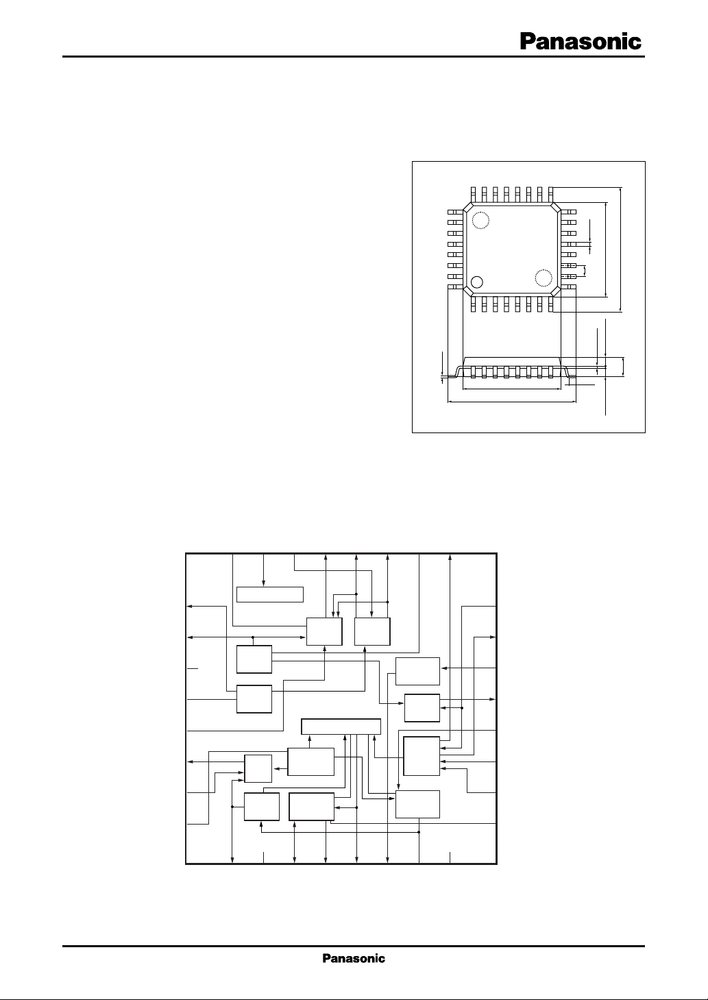
■ Block Diagram
FM-mix. in
FM-PIN D
24
23
22
21
20
19
18
24 17
25
32
18
0.1±0.1
7.0±0.3
9.2±0.4
LQFP032-P-0707
17
Unit : mm
16
–0.05
+0.10
0.3
7.0±0.3
0.8
9
–0.05
+0.10
0.15
(0.55)
0.625±0.100 0.625±0.100
9.2±0.4
1.4±0.2
V
FOSC
V
AOSC
GND2
Keyed-AGC in
AM-AF
OUT
25
26
27
28
29
30
31
32
FM/AM SW
AM
OSC
FE
OSC
AM
ATC
AM
det.
1
2
CC
V
FM
AGC
AM. S-meter
AM
IF AGC
AM
SSC
3
4
AM-SD out
AM-IF count
FM
mix.
IF amp.
IF amp.
5
6
AM-S. meter
FM
AM
mix.
AM
RF
AGC
AM
7
AM-IF out
16
15
14
13
12
11
10
9
8
GND1
1

AN7289NFBQ ICs for FM/AM Tuner
■ Pin Descriptions
Pin No. Description
1 AM detection output
2V
CC1
3 AM-IF counter output/DX/LO SW
4 AM-SD output
5 AM-signal meter output
6 FM-IF output
7 AM-IF output
8 GND1
9 SSC
10 AM-RF level detection
11 AM-WAGC detection/DX setting
12 AM-IF input
13 AM-mix. output
14 FM-IF input
15 AM-RF gain control
16 AM-mix. input
Pin No. Description
17 FM-PIN diode driver
18 AM-OSC coil pin
19 FM-mix. output 2
20 FM-mix. output 1
21 FM-PIN diode driver
22 FM-mix. input
23 V
/FM/AM SW
CC2
24 FM-AGC output
25 FM-OSC buffer output
26
AM-OSC buffer output/FE-AGC sensitivity setting
27 GND2
28 FM-OSC coil pin
29 FM-keyed-AGC input
30 AM-AM output/LO setting
31 AM-ATC input
32 AM-IF level detection
■ Absolute Maximum Ratings
Parameter Symbol Rating Unit
Supply voltage V
Supply current I
2
Power dissipation
Operating ambient temperature
Storage temperature
Note)*1: Ta = 25°C except power dissipation, operating ambient temperature and storage temperature.
2: Referring to "■ Technical Information" for power dissipation at Ta = 80°C, use the circuit under the conditions not exceeding
*
the allowable limit value.
*
1
*
1
*
CC
CC
P
D
T
opr
T
stg
9.1 V
56 mA
343.3 mW
−35 to +80 °C
−55 to +125 °C
■ Recommended Operating Range
Parameter Symbol Range Unit
Supply voltage V
CC
7.2 to 9.0 V
2
 Loading...