


Panasonic AN7208SA Datasheet
ICs for FM/AM Tuner
AN7208SA
TV/FM front-end IC for 1.5 V headphone stereo
■ Overview
The AN7208SA is a TV/ FM front-end IC developed
for use in the headphone stereo. It incorporates two
systems of FM and VHF band front-end. A pre-amp. between IF amp. is not necessary by combination with the
AN7233SH.
■ Features
• Built-in two system of FM and VHF band front-end
• Pre-amp. between IF amp. is not necessary (combina-
tion with the AN7233SH)
• Built-in standby /IF gain control/local oscillator buffer
circuits
■ Applications
• 1.5 V headphone stereo (VCC 1.0 V to 2.0 V)
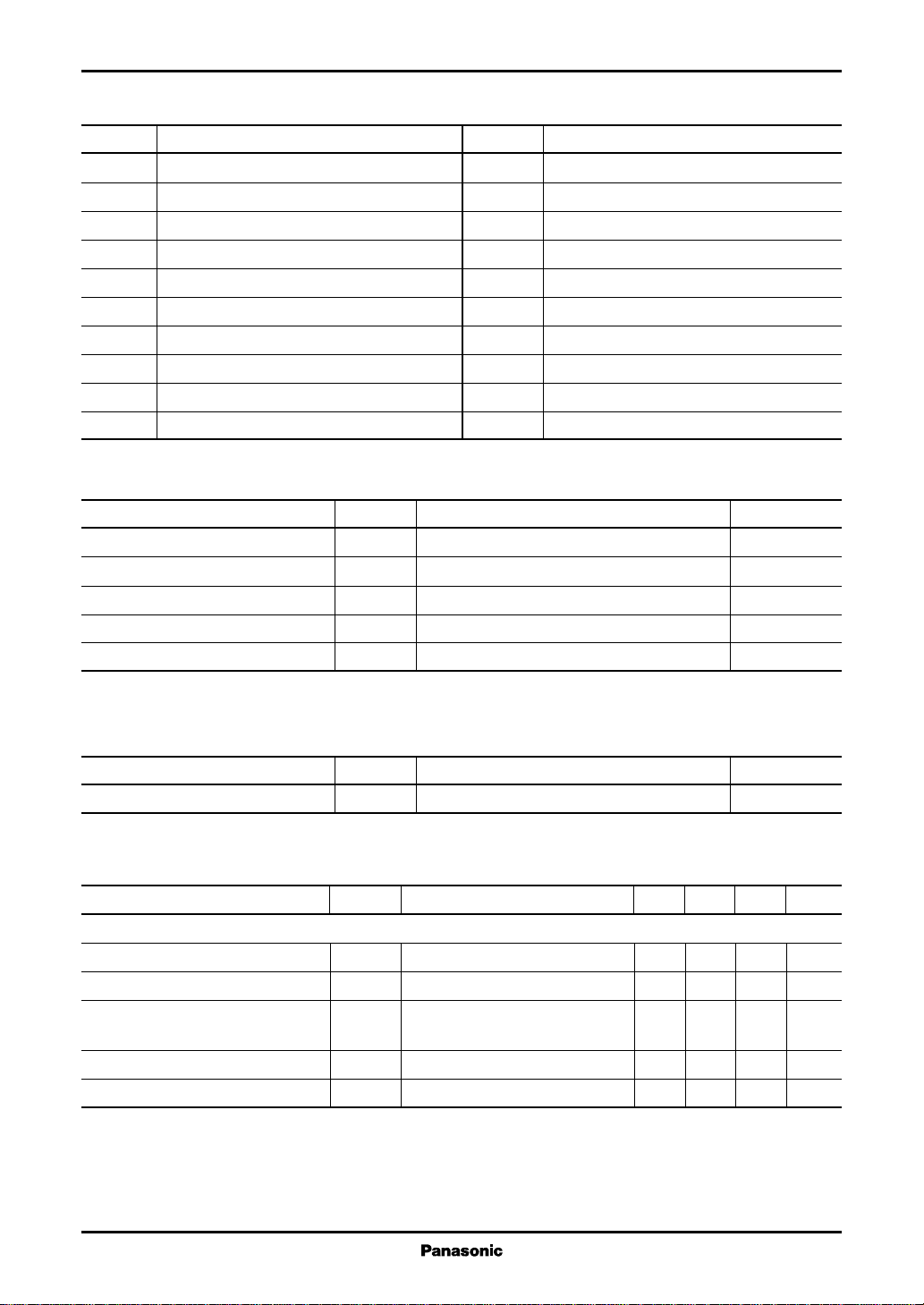
■ Block Diagram
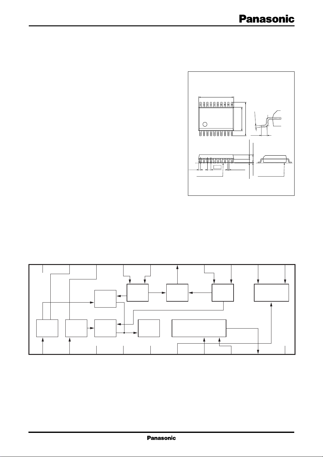
6.5±0.3
20 11
110
0.65
(0.33)
Seating plane
0.25±0.10
SSOP020-P-0225A
Unit : mm
− 0.05
+0.10
0.15
4.3±0.3
6.3±0.3
(0.50)
0.65±0.100.65±0.10
0.1±0.1 1.5±0.2
Seating plane
20
1
FM
RF
19
2
TV
RF
18
3
FM
mix.
TV
mix.
17
4
FM
OSC
16
1st
IF amp.
5
15
OSC
buffer
6
14
2nd
IF amp.
7
TV
OSC
13
8
12
9
11
Power
10
1
AN7208SA ICs for FM/AM Tuner
■ Pin Descriptions
Pin No. Description
1 FM RF input
2 TV RF input
3 GND 1
4N.C.
5 IF out 1
6 Mode SW
7 IF in
8 IF gain control
9 IF out 2
10 GND 2
■ Absolute Maximum Ratings
Parameter Symbol Rating Unit
Supply voltage V
Supply current I
Power dissipation P
1
Operating ambient temperature
1
Storage temperature
Note)*1 : All items are at Ta = 25°C, except for the operating ambient temperature and storage temperature.
*
*
CC
CC
D
T
opr
T
stg
Pin No. Description
11 V
CC2
12 STDBY
13 TV OSC 1
14 TV OSC 2
15 OSC buff.
16 FM OSC 1
17 FM OSC 2
18 TV RF
19 FM RF
20 V
CC1
2.5 V
12 mA
30 mW
−20 to +75 °C
−55 to +125 °C
■ Recommended Operating Range
Parameter Symbol Range Unit
Supply voltage V
CC
1.0 to 2.0 V
■ Electrical Characteristics at VCC = 1.2 V, Ta = 25°C
Parameter Symbol Conditions Min Typ Max Unit
TV fIN = 221.75 MHz
1
Conversion gain
Oscillation voltage V
2
*
S/N
Quiescent current I
Oscillation buffer output V
Note) Tuning is taken the peak point at 10.6 MHz output level ( VIN = 30 dBµ, non-modulation)
1 : Conversion gain = 20 Log( ∆V (µV) ÷ 31.6)
*
∆V is the output difference at VIN = 30 dBµ and at VIN = 36 dBµ
2 : Measurement is done at the detection output of the AN7233
*
Measure the ratio of output at f
2
*
G
CONV(TV)fOUT
OSC(TV)VCC
S/N
(TV)
= 10.6 MHz 30 38 46 dB
= 0.95 V 15 27
Input level = 60 dBµ 41 44 dB
1 kHz 30% Mod.
TOT(TV)
BUF(TV)VCC
= 22.5 kHz to that at f
DIV
8.8 12 mA
= 0.95 V 39 62
= 0 Hz (modulation freq. 1 kHz)
DIV
mV[rms]
mV[rms]
ICs for FM/AM Tuner AN7208SA
■ Electrical Characteristics at VCC = 1.2 V, Ta = 25°C (continued)
Parameter Symbol Conditions Min Typ Max Unit
TV fIN = 221.75 MHz (continued)
3
Burst noise
*
FM fIN = 107.88 MHz
1
Conversion gain
*
Oscillation voltage V
2
*
S/N
Quiescent current I
Oscillation buffer output V
3
Burst noise
Note) Tuning is taken the peak point at 10.6 MHz output level ( VIN = 30 dBµ, non-modulation)
*
1 : Conversion gain = 20 Log( ∆V (µV) ÷ 31.6)
*
∆V is the output difference at VIN = 30 dBµ and at VIN = 36 dBµ
2 : Measurement is done at the detection output of the AN7233
*
Measure the ratio of output at f
3 : Measurement is done at the detection output of the AN7233
*
Measures a peak voltage of the measurement time = within 500 ms (OK to 10 times)
V
NO(TV)
Input level = 60 dBµ−1.8 1.8
Non-modulation
G
CONV(FM)fOUT
OSC(FM)VCC
S/N
Input level = 60 dBµ 48 51 dB
(FM)
1 kHz 30% mod.
TOT(FM)
BUF(FM)VCC
V
NO(FM)
Input level = 60 dBµ−1.8 1.8
Non-modulation
= 22.5 kHz to that at f
DIV
mV[p-0]
= 10.6 MHz 30 38 4 6 dB
= 0.95 V 40 63
mV[rms]
7.7 1 0 mA
= 0.95 V 66 132
mV[rms]
mV[p-0]
= 0 Hz (modulation freq. 1 kHz)
DIV
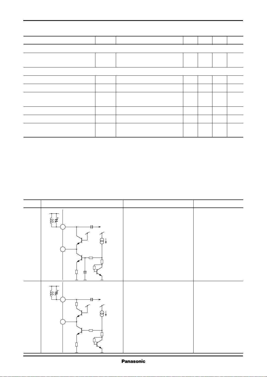
■ Terminal Equivalent Circuits
Pin No. Equivalent circuit Description
1 FM RF input Approx. VCC − 0.7 V
19
To mix.
RF signal input in FM band
(Common base type)
1
2 TV RF input Approx. VCC − 0.7 V
18
To mix.
RF signal input in TV band
(Common base type)
2
Input resistance or pin voltage
3