

Panasonic AN7199Z Datasheet
ICs for Audio Common Use
AN7199Z
Dual 20 W BTL power IC for car audio
■ Overview
The AN7199Z is an audio power IC developed for the
sound output of car audio (dual 20 W).
A capacitor and a resistor to stop oscillation are built
in between the output pin and GND so that a space saving of set is possible. Also, it is incorporates an industry's
first superior muting circuit which is free from shock
noise, so that a shock noise design under the set transient
condition can be made easily when the muting circuit is
used together with its standby function.
In addition, it is incorporating various protective circuits to protect the IC from destruction by GND-open
short-circuit to GND and power supply surge which are
the most important subjects of power IC protection, and
the IC will largely contribute to a high reliability design
of equipment.
■ Features
• Built-in various protection circuits (realizing high break-
down voltage against destruction)
Power supply surge breakdown voltage of 80 V or more
Ground open breakdown voltage of 16 V or more
• Built-in standby function (free from shock noise when
STB-on/off)
• Built-in muting function
Free from shock noise at mute-on/off
• Adapting attenuator method so that abnormal sound due
to waveform deformation is not generated
Attack time, recovery time of 50 ms or less
• Reduction in external components
No CR for oscillation stop is required
It eliminates the need for NF and BS electrolytic capacitors
Muting function is unneccesary
Power supply choke coil is unnecessary
• Provided with beep sound input pin
• High sound quality design
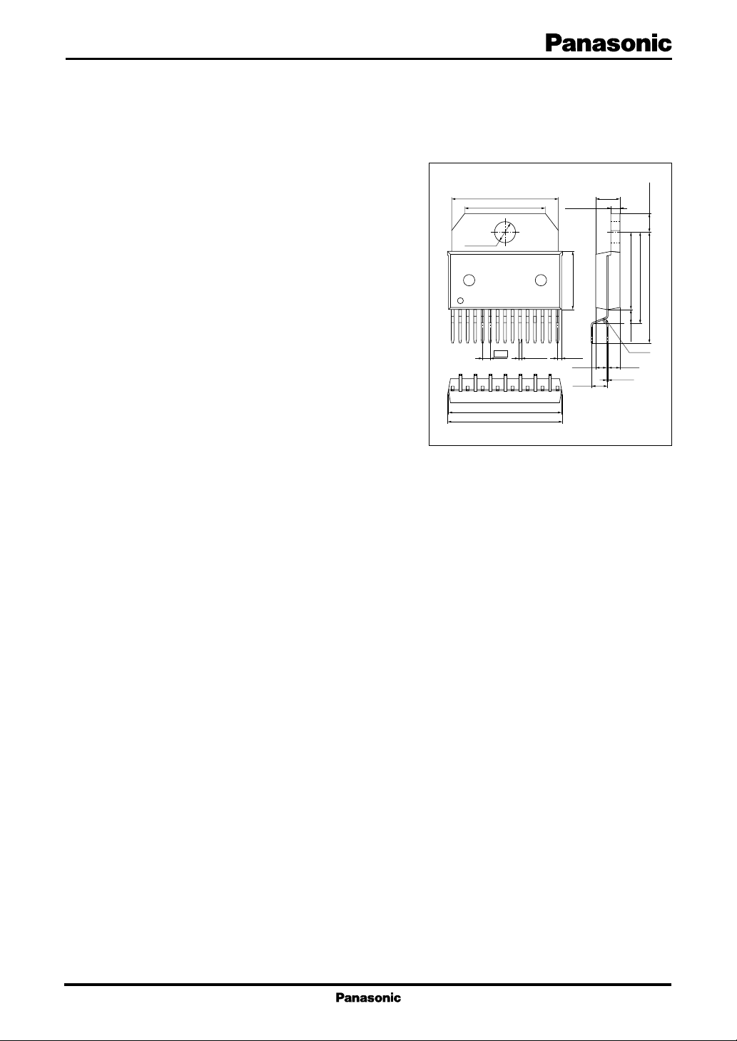
Unit : mm
18.00±0.30
13.50±0.30
φ3.60±0.10
115
19.00±0.30
19.30±0.30
1.27
0.50
+0.20
–0.10
4.00±0.20
1.50±0.10
10.0±0.30
(0.61)
(1.80) (1.95)
0.25
(2.54)
13.25±0.30
2.40±0.50
R0.55
+0.15
–0.05
3.25±0.10
15.65±0.50
18.95±0.50
HZIP015-P-0745A
■ Applications
• Car audio
1
AN7199Z ICs for Audio Common Use
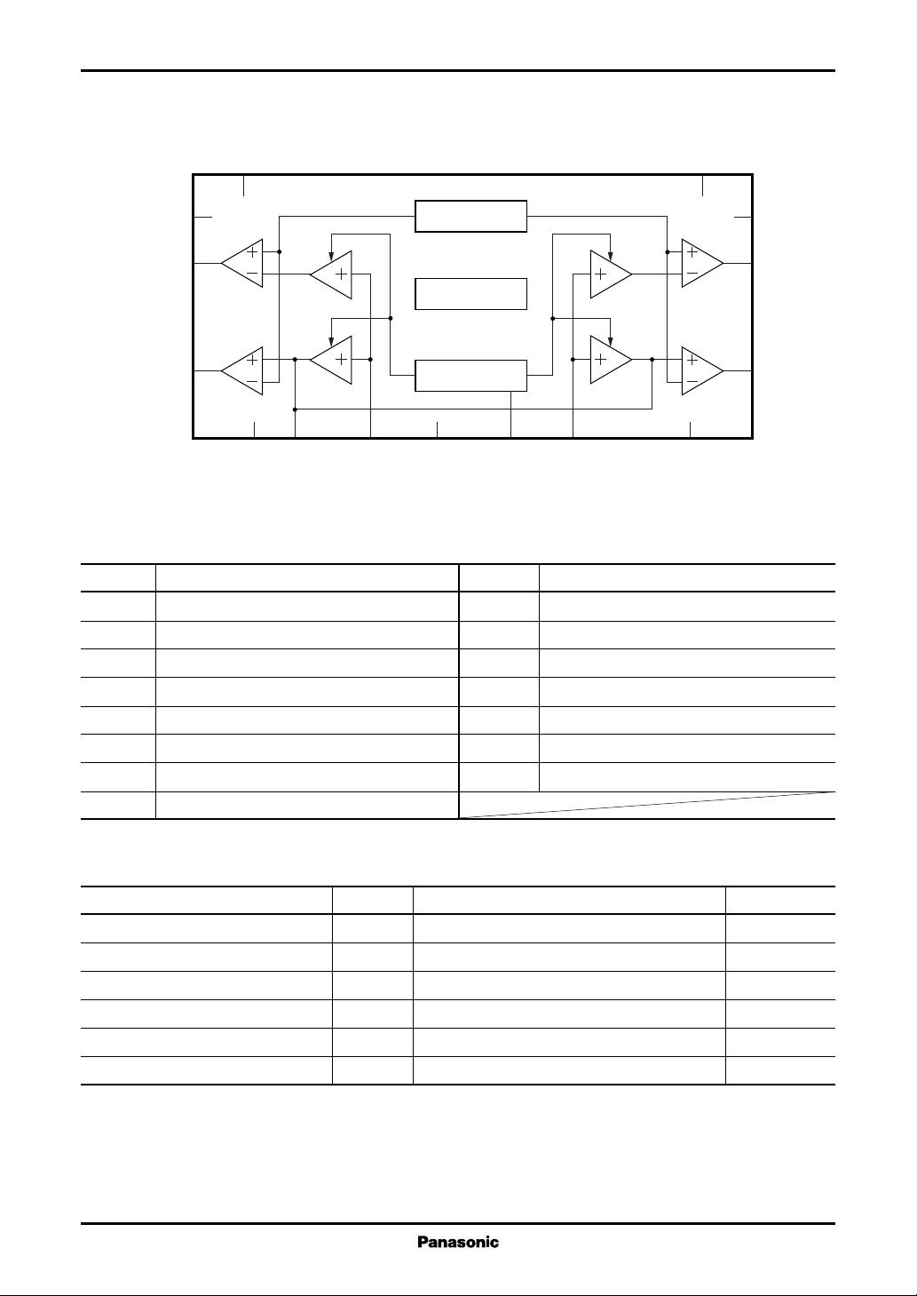
■ Block Diagram
CC
V
1
Ch.1 GND Ch.2 GND
Ch.1 Out (−)
3
4
Att.
Ch.1 Out (+)
2
Att.
8
10
6
Ref.
Protection Cct.
Att.Con.
5
7
Att.
Att.
11
Ripple filter
12
14
13
15
9
Mute
Beep In
GND(sub)
Ch.1 In
Standby
Ch.2 In
GND(input)
■ Pin Descriptions
Pin No. Description
1 Power supply
2 Ch.1 output (+)
3 Grounding (output ch.1)
4 Ch.1 output (−)
5 Standby
6 Ch.1 input
7 Muting
8 Grounding (sub)
Pin No. Description
9 Grounding (input)
10 Beep sound input
11 Ch.2 input
12 Ripple filter
13 Ch.2 output (−)
14 Grounding (output ch.2)
15 Ch.2 output (+)
Ch.2 Out (−)
Ch.2 Out (+)
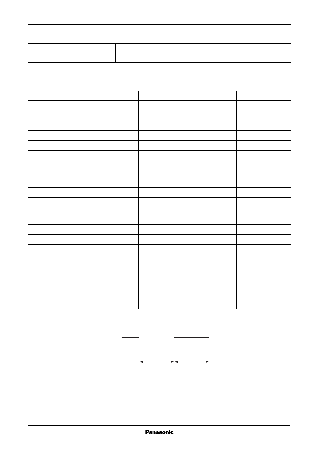
■ Absolute Maximum Ratings
Parameter Symbol Rating Unit
2
Supply voltage
Peak supply voltage
Supply current I
Power dissipation
Operating ambient temperature
Storage temperature
Note)*1 : All items are at Ta = 25°C, except for the operating ambient temperature and storage temperature.
2 : Without signal
*
3 : Time = 0.2 s
*
4: Ta = 85°C
*
2
*
3
*
4
*
1
*
1
*
V
CC
V
surge
CC
P
D
T
opr
T
stg
25 V
60 V
9.0 A
59 W
−30 to +85 °C
−55 to +150 °C
ICs for Audio Common Use AN7199Z
■ Recommended Operating Range
Parameter Symbol Range Unit
Supply voltage V
CC
■ Electrical Characteristics at VCC = 13.2 V, f = 1 kHz, Ta = 25°C
Parameter Symbol Conditions Min Typ Max Unit
Quiescent current I
Standby current I
1
Output noise voltage
*
V
Voltage gain 1 G
Total harmonic distortion 1 THD1V
Maximum output power 1 P
1
Ripple rejection ratio
*
Channel balance CB V
1
Cross-talk
*
Output offset voltage V
1
Muting effect
*
MT VO = 1 W, RL = 4 Ω 70 86 dB
Input impedance Z
Voltage gain 2 G
Total harmonic distortion 2 THD2VIN = 20 mV, RL = 2 Ω0.12 0.5 %
Maximum output power 2 P
2
Shock noise
*
Total harmonic distortion 3 THD
Note)*1 : Measurement using a bandwidth 15 Hz to 30 kHz (12 dB/OCT) filter.
2 : For V
*
= on/off, change over the standby terminal by the voltages of 0 V and 5 V at the time shown below.
STB
VIN = 0 mV, RL = 4 Ω120 250 mA
CQ
VIN = 0 mV, RL = 4 Ω110µA
STB
Rg = 10 kΩ, RL = 4 Ω0.18 0.5
NO
V
V1
O1
= 20 mV, RL = 4 Ω 38 40 42 dB
IN
= 20 mV, RL = 4 Ω0.07 0.4 %
IN
THD = 10%, RL = 4 Ω 16 18.5 W
V
= 14.4 V, RL = 4 Ω22.0 W
CC
RR RL = 4 Ω, Rg = 10 kΩ,5560 dB
Vr = 1 V[rms], fr = 1 kHz
= 20 mV, RL = 4 Ω01dB
IN
CT VIN = 20 mV, RL = 4 Ω,6079 dB
Rg = 10 kΩ
Rg = 10 kΩ, RL = 4 Ω−300 0 300 mV
Off
VIN = ± 0.3 V
i
VIN = 20 mV, RL = 2 Ω 38 40 42 dB
V2
THD = 10%, RL = 2 Ω 16 25 W
O2
V
RL = 4 Ω, Rg = 10 kΩ−100 0 100
S
V
= on/off, 50 Hz HPF-on
STB
= 10 mV, fIN = 20 kHz 0.10 0.5 %
3VIN
Rg = 10 kΩ, RL = ∞
8.0 to 18.0 V
DC
24 30 36 kΩ
mV[rms]
mV[p-0]
Standby terminal voltage
5 V
0 V
500 ms 500 ms
3

AN7199Z ICs for Audio Common Use
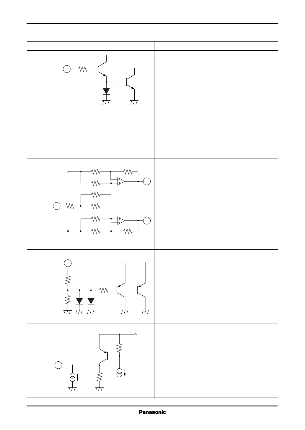
■ Terminal Equivalent Circuits
Pin No. Equivalent circuit Description DC Voltage
1 Supply voltage pin 13.2 V
Supply connection pin
2 Ch.1 output pin (+) 6.6 V
1
Drive circuit
2
Drive circuit
3
15 kΩ
AN7198Z : 600 Ω
AN7199Z : 300 Ω
3 GND (output) 0 V
4 Ch.1 output pin (−) 6.6 V
1
Drive circuit
4
V
REF
Pre-amp.
Ch.1 positive-phase output pin
= 6.3 V
Grounding pin for ch.1 output
Pre-amp.
Ch.1 inverted-phase output pin
= 6.3 V
V
REF
Drive circuit
3
15 kΩ
AN7198Z : 600 Ω
AN7199Z : 300 Ω
5 Standby control pin
5
10 kΩ
Standby changeover pin
Threshold voltage approx. 2.1 V
2 kΩ
6 Ch.1 input pin
6
200 Ω
Approx.
600 Ω
15 µA
Approx.
15 µA
Ch.1 input signal applied pin
Input impedance 30 kΩ
30 kΩ
0 mV to10 mV
4
ICs for Audio Common Use AN7199Z
■ Terminal Equivalent Circuits (continued)
Pin No. Equivalent circuit Description DC Voltage
7 Mute control pin
7
200 Ω
Mute changeover pin
Threshold voltage approx. 2.1 V
8 GND (substrate) 0 V
Being connected with substrate only
9 GND (input) 0 V
Ground pin for input
10 Beep sound input pin 2.1 V
V
= 6.3 V
REF
7.8 kΩ
R
nf
R
nf
15 kΩ
15 kΩ
15 kΩ
Beep sound signal input pin
2
Input impedance 15.3 kΩ
10
R
nf
V
REF
= 6.3 V
R
nf
15 kΩ
15
RnfAN7198Z : 600Ω
AN7199Z : 300Ω
11 Ch.2 input pin
0 mV to10 mV
11
200 Ω
Approx.
600 Ω
15 µA
Approx.
15 µA
Ch. 2 input signal applied pin
Input impedance 30 kΩ
30 kΩ
12 Ripple filter pin 13.0 V
V
CC
15 kΩ
Output current 3 mA to 10 mA
12
350 µA
1.7 mA
20 kΩ
5
AN7199Z ICs for Audio Common Use
■ Terminal Equivalent Circuits (continued)
Pin No. Equivalent circuit Description DC Voltage
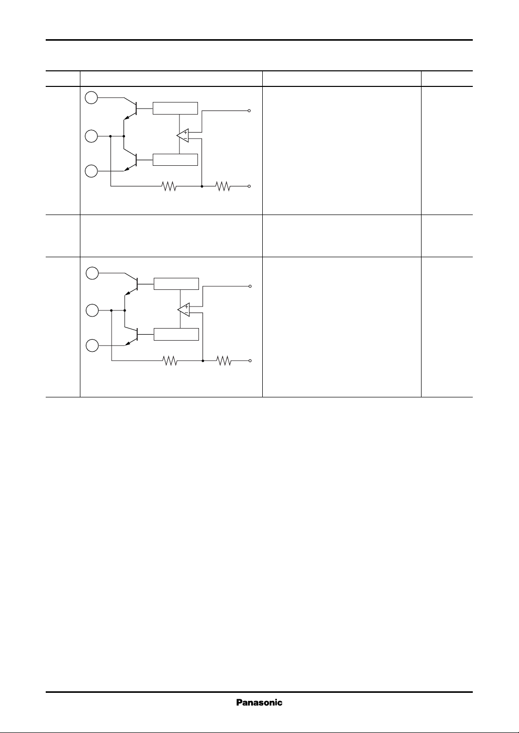
13 Ch.2 output pin (−) 6.3 V
1
Drive circuit
Pre-amp.
Ch.2 inverted-phase output pin
13
V
REF
= 6.3 V
15
Drive circuit
15 kΩ
AN7198Z : 600 Ω
AN7199Z : 300 Ω
14 GND(output) 0 V
Grounding pin for ch.2 output
15 Ch.2 output pin (+) 6.3 V
1
Drive circuit
Pre-amp.
Ch.2 positive-phase output pin
14
= 6.3 V
V
REF
15
Drive circuit
15 kΩ
AN7198Z : 600 Ω
AN7199Z : 300 Ω
■ Usage Notes
1. Always attach an outside heat sink to use the chip. In addition, the outside heat sink must be fastened onto a
chassis for use.
2. Connect the cooling fin to GND potential.
3. Avoid short-circuit to V
a special condition.
4. The temperature protection circuit will be actuated at Tj = approx. 150°C, but it is automatically reset when the
chip temperature drops below the above set level.
5. The overvoltage protection circuit starts its operation at VCC = approx. 20 V.
6. Take into consideration the heat radiation design particularly when V
7. When the beep sound function is not used, open the beep sound input pin (pin 10) or connect it to pin 9 with
around 0.01 µF capacitor.
8. Connect only pin 9 (ground, signal source) to the signal GND of the amplifier in the previous stage. The
characteristics such as distortion, etc. will be improved.
6
and short-circuit to GND, and load short-circuit. There is a danger of destruction under
CC
is set high or when the load is 2 Ω.
CC
 Loading...