

Panasonic AN7195K Datasheet
ICs for Audio Common Use
AN7195K
Dual 15 W BTL power IC for car audio
■ Overview
The AN7195K is an audio power IC developed for the
sound output of car audio (dual 15 W).
It is incorporating various protection circuits to protect the IC from destruction by GND-open short-circuit
to GND and power supply surge which are the most important subjects of power IC protection, and the IC will
largely contribute to a high reliability design of equipment.
It is also incorporating the industry's first excellent
muting circuit, which is free from shock noise, so that a
shock noise design under the set transient condition can
be made easily when the muting circuit is used together
with its standby function.
In addition, the AN7195K is pin compatible with the
AN7190NK (dual 20 W), so that the identical pattern
design is allowed for high-class types as well as popular
types.
■ Features
• Built-in various protection circuits (realizing high break-
down voltage against destruction )
Power supply surge breakdown voltage of 100 V or more
Ground -open breakdown voltage of 14 V or more
• Built-in standby function (free from shock noise at
standby on/off)
• Built-in muting function
Free from shock noise at mute-on/off
Adapting attenuator method so that abnormal sound due
to waveform deformation is not generated
Attack time, recovery time of 50 ms or less
• Reduction in external components (parts reduction to
half compared with the AN7176K)
It eliminates the need for NF and BS electrolytic capacitors,
Muting function is unnecessary
Power supply choke coil is unnecessary
• Provided with beep sound input pin
• High sound quality design
• Pin compatible with the AN7190NK (dual 20 W)
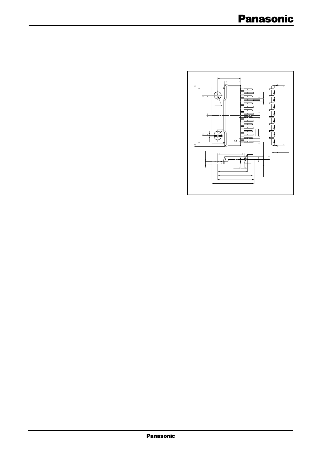
28.0±0.3
29.75±0.3
(10.0)
20.0±0.3
(10.0)
1.2+0.1
φ3.6
R1.8
(0.6)
11.3±0.3
7.7±0.3
16
1
(12.5)
R0.7
(1.2)
(14.1)
(17.63)
(18.7)
(21.5)
HZIP016-P-0665A
Unit : mm
0.10
+0.15
-
(1.1)
0.6
(0.889)
(0.889)
1.788
1.45±0.151.80±0.15
0.05
+0.10
-
0.25
29.6±0.3
3.5±0.2
(2.54)
■ Applications
• Car audio
1
AN7195K ICs for Audio Common Use
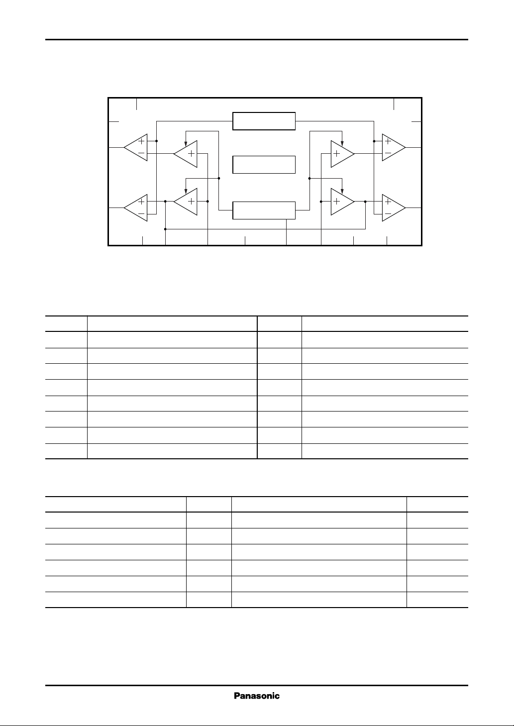
■ Block Diagram
CC
V
1
Ch.1 GND Ch.2 GND
Ch.1 Out (−)
3
4
Att.
Ch.1 Out (+)
2
Att.
8
10
Beep In
6
Ch.1 In
Ref.
Protection Cct.
Att.Con.
5
7
Standby
Mute
11
Ch.2 In
Att.
Att.
16
N.C.
GND(sub)
Ripple filter
12
14
13
15
9
GND(input)
■ Pin Descriptions
Pin No. Description
1 Power supply
2 Ch.1 output (+)
3 Grounding (output ch.1)
4 Ch.1 output (−)
5 Standby
6 Ch.1 input
7 Muting
8 Grounding (sub)
Pin No. Description
9 Grounding (input)
10 Beep sound input
11 Ch.2 input
12 Ripple filter
13 Ch.2 output (−)
14 Grounding (output ch.2)
15 Ch.2 output (+)
16 N.C.
Ch.2 Out (−)
Ch.2 Out (+)
■ Absolute Maximum Ratings
Parameter Symbol Rating Unit
2
Supply voltage
Peak supply voltage
Supply current I
Power dissipation
Operating ambient temperature
Storage temperature
Note)*1 : All items are at Ta = 25°C, except for the operating ambient temperature and storage temperature.
2 : Without signal
*
3 : Time = 0.2 s
*
4: Ta = 85°C
*
2
*
3
*
*4
1
*
1
*
V
CC
V
surge
CC
P
D
T
opr
T
stg
25 V
80 V
9.0 A
32.5 W
−30 to +85 °C
−55 to +150 °C
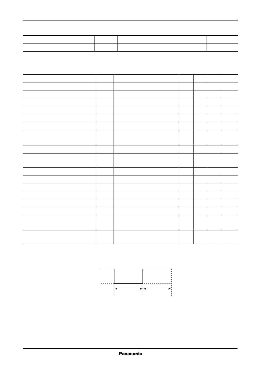
ICs for Audio Common Use AN7195K
■ Recommended Operating Range
Parameter Symbol Range Unit
Supply voltage V
CC
■ Electrical Characteristics at VCC = 13.2 V, f = 1 kHz, Ta = 25°C
Parameter Symbol Conditions Min Typ Max Unit
Quiescent current I
Standby current I
1
Output noise voltage
*
V
Voltage gain 1 G
Total harmonic distortion 1 THD1V
Maximum output power 1 P
1
Ripple rejection ratio
*
Channel balance CB V
Cross-talk
*1
Output offset voltage V
1
Muting effect
*
MT VIN = 20 mV, RL = 4 Ω 70 82 dB
Input impedance Z
Voltage gain 2 G
Total harmonic distortion 2 THD2VIN = 20 mV, RL = 2 Ω0.1 0.5 %
Maximum output power 2 P
2
Shock noise
*
Total harmonic distortion 3 THD
Note)*1 : Measurement using a bandwidth 15 Hz to 30 kHz (12 dB/OCT) filter.
2 : For V
*
= on/off, change over the standby terminal by the voltages of 0 V and 5 V at the time shown below.
STB
VIN = 0 mV, RL = 4 Ω120 250 mA
CQ
VIN = 0 mV, RL = 4 Ω110µA
STB
Rg = 4.7 kΩ, RL = 4 Ω0.22 0.5
NO
V
V1
O1
= 20 mV, RL = 4 Ω 38 40 42 dB
IN
= 20 mV, RL = 4 Ω0.07 0.4 %
IN
THD = 10%, RL = 4 Ω 12 14 W
RR RL = 4 Ω, Rg = 4.7 kΩ,6070 dB
Vr = 1 V[rms], fr = 1 kHz
= 20 mV, RL = 4 Ω01dB
IN
CT VIN = 20 mV, RL = 4 Ω,5565 dB
Rg = 4.7 kΩ
Rg = 4.7 kΩ, RL = 4 Ω−300 0 300 mV
Off
VIN = ± 0.3 V
i
VIN = 20 mV, RL = 2 Ω 38 40 42 dB
V2
THD = 10%, RL = 2 Ω 12 20 W
O2
V
RL = 4 Ω, Rg = 4.7 kΩ−100 0 100
S
V
= on/off, 50 Hz HPF-on
STB
= 10 mV, fIN = 20 kHz 0.10 0.5 %
3VIN
Rg = 4.7 kΩ, RL = ∞
8.0 to 18.0 V
DC
22 30 35 kΩ
mV[rms]
mV[p-0]
Standby terminal voltage
5 V
0 V
500 ms 500 ms
3
AN7195K ICs for Audio Common Use
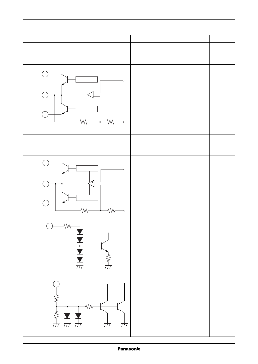
■ Terminal Equivalent Circuits
Pin No. Equivalent circuit Description DC Voltage
1 Supply voltage pin 13.2 V
Supply connection pin
2 Ch.1 output pin (+) 6.6 V
1
Drive circuit
2
Drive circuit
3
15 kΩ 300 Ω
3 GND (output) 0 V
4 Ch.1 output pin (−) 6.6 V
1
Drive circuit
Pre-amp.
V
REF
Pre-amp.
Ch.1 positive-phase output pin
= 6.6 V
Grounding pin for ch.1 output
Ch.1 inverted-phase output pin
4
V
= 6.6 V
Drive circuit
3
15 kΩ 300 Ω
REF
5 Standby control pin
5
10 kΩ
Standby changeover pin
Threshold voltage approx. 2.1 V
900 Ω
6 Ch.1 input pin
6
200 Ω
Approx.
400 Ω
15 µA
Approx.
15 µA
Ch.1 input signal applied pin
Input impedance 30 kΩ
30 kΩ
0 mV to10 mV
4
 Loading...