

Panasonic AN2492FH Datasheet
ICs for VCR
AN2492FH
Luminance and chrominance signal processing circuit for
8 mm video (NTSC)
■ Overview
The AN2492FH is a single chip LSI on which Y/C
main signal processing circuit of NTSC normal 8 mm
VCR is integrated. It is possible to reduce the system
cost drastically thanks to the introduction of an external
filter on to the chip and fc auto adjustment.
■ Features
• 5 V single power supply
• Reduction of the external components and adjusting
parts by adopting automatic adjustment filter
• No need of glass delay lines
• For NTSC (PAL: AN2493 pin-compatible)
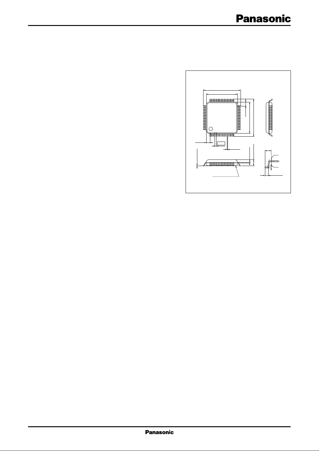
49
64
(1.25)
0.10±0.10
12.00±0.20
10.00±0.20
48 33
0.50
0.18
Seating plane
32
17
161
+0.10
−0.05
(1.25)
+0.10
10.00±0.20
−0.05
0.15
12.00±0.201.95±0.20
Unit: mm
(1.00)
0° to 10°
0.50±0.20
■ Applications
• 8 mm VCR, 8 mm video camera
QFP064-P-1010
1

AN2492FH ICs for VCR
■ Block Diagram
CTL
NL in
LNC out
CCL det.
CDL in
G1 det.
ADD out
CTL1
CONP C
L IMC
To CCD
G2 det.
YDL in
YCL det.
CL in
ML out
Y GND
Video out
Y V
VNF
VF mute CTL
VF out
V mute CTL
Clamp det.
Line in
ME out
W CTL
ME NF
25
27
26
Clamp
HSS
SW 12
PR
N.C.
HPF
LIM
28
Amp.
29
(COR det. out)
24
W/D
0
f
23222120191817
Smear
DEV CTL
MOD
GCA3 CTL
FM out (DOC)
GCA3
HPF1
30
GCA1
31
Clamp
32
33
34
35
V mute
Mute
36
37
38
GCA2
Trap
39
40
Clamp
41
42
SW 4
NOR PS
43
44
CC
Sub 2
SW 8
ATT
CORR
BPF
SW 18
P
R
SW 11
MIX
(d)
R
N
Sync.
DOC
SW 5
CNR
LIM
Line
Det.
CTL
C
A
Clamp
CONP
Det.
SW 6
PB
P
CONP
SW 2
Chroma
PB
Line
SW 15
DE/EM
P
P
R
45
46
47
OSD
SW 1
OSD
Main
LPF
SW 3
P
R
C
ATT
PBY
DL
48
OSD
49
50
SW 21
51
AGC det.
SW 0
SW 19
R
AGC
52
Clamp
P
CONP Y
SS
AGC
det.
Test 9
54
53
55
SS det.
56
SS out
RF AGC
57
FM in
RF det.
58
REC PB VOL
DOC
RF out
MA in
LIM
D LIM
59
D LIM in
DEMOD
Sub
60
MDE
LPF
61
MDC
DCL Amp. Amp.
62
DCL in
Clip
63
Clip in
90 PS
64
out
VXO
CEC det.
CE CTL
R
SW 16
1/46 1/8
Sub BM
VXO
1
VXO in
PB C in
C sub
P
R
ACC
R
BM
Burst
DE/EM
SLD
REC APC
2
REC APC det.
LPF
LPF
P
P
DP PC
R
SW 14
SW 17
REC
V
3
det.
V
SW 13
AFC
4DIV
F PC
REF
REF
CACC
CK PC
1/4
4
Trap
LPF
ACC det.
CK
PBA PC
out
SC
f
HPF
GCA4
1/8 CL det.
1/4
VCO
f det.
1/8
16
CK
15
14
13
12
11
10
9
8
7
6
5
GCA4 CTL
REC C out
CLCA det.
PB C out
C MIX in
C GND
Data
CK
C V
CC
PG in
PB APC det.
f
det.
2
ICs for VCR AN2492FH
■ Pin Descriptions
Pin No. Description
1 VXO in
2 REC APC det.
3V
4f
det.
REF
out
SC
5 f det.
6 PB APC det.
7 PG in.
8C V
CC
9CK
10 Data
11 C GND
12 C MIX in
13 PB C out
14 CLCA det.
15 REC C out
16 GCA4 CTL
17 PB C in
18 CEC det.
19 Chroma emph. CTL
20 GCA3 CTL (APT CTL)
21 FM out (DOC)
22 DEV CTL
23 f0 CTL
24 ME out (COR det. out)
25 W CTL
26 MENF
27 NL in
28 LNC out
29 CCL det.
30 CDL in
31 G1 det.
32 ADD out
Pin No. Description
33 GCA1 CTL
34 CONP C
35 LIMC
36 To CCD
37 G2 det.
38 YDL in
39 YCL det.
40 CL in
41 ML out
42 Y GND
43 Video out
44 Y V
CC
45 VNF
46 VF mute CTL
47 VF out (BGP out)
48 V mute CTL
49 Clamp det.
50 Line in
51 AGC det.
52 CONP Y
53 REC PB VOL
54 SS det.
55 SS out
56 RF det.
57 FM in
58 RF out
59 DLIM in
60 MD E
61 MD C
62 DCL in
63 Clip in
64 VXO out
3
AN2492FH ICs for VCR
■ Absolute Maximum Ratings
Parameter Symbol Rating Unit
Supply voltage V
Supply current I
2
Power dissipation
Operating ambient temperature
Storage temperature
Note)*1: Except for the power dissipation, operating ambient temperature and storage temperature, all ratings are for Ta = 25°C.
2: The power dissipation shown is for the IC package at Ta = 70°C.
*
PD = 696 (mW) (Ta = 70°C) in mounting on the glass epoxy printed circuit board of 50 × 50 × 0.8 (mm).
3: PD = 471 (mW) at supply voltage VCC = 4.8 V.
*
*
*1, *
1
*
CC
CC
P
D
3
T
opr
T
stg
■ Recommended Operating Range
Parameter Symbol Range Unit
5.5 V
100 mA
359 mW
−10 to +70 °C
−55 to +125 °C
Supply voltage V
CC
■ Electrical Characteristics at VCC = 4.8 V, Ta = 25°C
Parameter Symbol Conditions Min Typ Max Unit
Consumption current 1 I
Consumption current 2 I
Consumption current 3 I
Consumption current 4 I
Internal reference voltage source V
REC overall V
Y-AGC control characteristics ∆V
Y-AGC through mode V
View finder amp. frequency f
characteristics at input 100 kHz, 5 MHz
Video-OSD white mute level V
Video-OSD black mute level V
Video-OSD white mute CTL V
voltage character
Video-OSD black mute CTL V
voltage character
Video-OSD through CTL voltage
V
Consumption current for recording 52 72 92 mA
CC1
Consumption current for playback 58 78 98 mA
CC2
Power save mode 42 62 82 mA
CC3
Camera power save mode −8 −4.2 −1mA
CC4
Pin 3 voltage 2.5 V
REF
Adjust pin 53 to set pin 47 output −14 −12 −10 dB
ME
at 1 V[p-p]
Pin 47 output gain ratio with input −1.5 0 1.5 dB
AGC
0.5 V[p-p] and 2.0 V[p-p]
Pin 24 output at pin 50 input 200 250 300 mV[p-p]
26S
Output ratio of 5 MHz/100 kHz −1.5 0 1.5 dB
BA
DC voltage based on a pedestal level 56 68 80 IRE
OW
DC voltage based on a pedestal level −7 0 12 IRE
OB
Pin 48 input at inserting a record 3.6 4.8 V
48W
Pin 48 input at inserting a record 2.0 2.6 V
48B
Pin 48 input at inserting a record 0 1.0 V
48S
character
4.7 to 5.2 V
4
ICs for VCR AN2492FH
■ Electrical Characteristics at VCC = 4.8 V, Ta = 25°C (continued)
Parameter Symbol Conditions Min Typ Max Unit
Video-OSD quasi V level V
Video-OSD quasi V mute CTL V
voltage
Video-OSD through CTL V
voltage
Y-main-LPF frequency Df
characteristics 1 Output: 2.5 MHz/100 kHz
Y-main-LPF frequency Df
characteristics 2 Output: 3.58 MHz/100 kHz
Video amp. output amplitude V
Video amp. frequency f
characteristics Output: 5 MHz/100 kHz
View finder OSD white mute level
View finder OSD black mute level
V
V
View finder OSD white mute V
CTL voltage the display characters
View finder OSD black mute V
CTL voltage the display characters
View finder OSD through CTL V
voltage the display characters
View finder OSD quasi V level V
View finder OSD quasi V mute V
CLT voltage
View finder OSD through CTL V
voltage
PB OSD white mute level V
PB OSD black mute level V
PB OSD white mute CTL V
voltage the display characters
PB OSD black mute CTL V
voltage the display characters
PB OSD through CTL voltage V
PB OSD off V
Sync. separation min. input V
sensitivity
Sync. separation pulse delay t
amount pin 40 and pin 55
DC voltage difference based on sync. −100 −50 0 mV
OV
tip in PB mode
PB mode, pin 48 input 2.0 4.8 V
48V
PB mode, pin 48 input 0 1.0 V
48G
Input: 100 kHz, 2.5 MHz −5 −22 dB
ML1
Input: 100 kHz, 3.58 MHz −25 dB
ML2
VF out 1 V[p-p] adjustment 1.75 2.0 2.25 V[p-p]
VO
Input: 100 kHz, 5 MHz −1.5 0 1.5 dB
VI
DC voltage based on a pedestal level 56 68 80 IRE
BOW
DC voltage based on a pedestal level −7 0 12 IRE
BOB
Pin 48 = 0 V at inserting 3.6 4.8 V
46W
Pin 48 = 0 V at inserting 2.0 2.6 V
46B
Pin 48 = 0 V at inserting 0 1.0 V
46S
DC voltage based on sync. tip in −60 −20 20 mV
BOV
PB mode
PB mode, pin 48 input 2.0 4.8 V
B48V
PB mode, pin 48 input 0 1.0 V
B48S
DC voltage based on a pedestal level 56 68 80 IRE
POW
DC voltage based on a pedestal level −7 0 12 IRE
POB
Pin 48 = 0 V at inserting 3.6 4.8 V
46W
Pin 48 = 0 V at inserting 2.0 2.6 V
46B
Pin 48 = 0 V at inserting 0 1.0 V
46S
the display characters
Pin 48 = 0 V at inserting 1.75 2.0 2.25 V[p-p]
VOO
the display characters
Input sync. level 65 mV[p-p]
SS
Measurement of sync. delay at 560 760 960 ns
SS
5
AN2492FH ICs for VCR
■ Electrical Characteristics at VCC = 4.8 V, Ta = 25°C (continued)
Parameter Symbol Conditions Min Typ Max Unit
Sync. separation output amplitude 1
Sync. separation output amplitude 2
Non linear emphasis 1 f
Non linear emphasis 2 f
Non linear emphasis 3 f
Non linear de-emphasis 1 f
Non linear de-emphasis 2 f
Non linear de-emphasis 3 f
Dark clip level V
White clip level V
FM carrier interleave V
FM modulator oscillation frequency
FM modulator deviation CTL f
FM modulator secondary distortion
Y-FM-GCA output amplitude 1 V
Y-FM-GCA output amplitude 2 V
PB-Y-RFAGC output amplitude V
PB-Y-RFAGC output secondary distortion
PB-over-all 1 (NOR) V
FM demodulation linearity 1 ∆V
Dropout detection on level V
Dropout detection off hysteresis ∆V
Dropout detection ENV off V
Dropout detection output high-level
Dropout detection output low-level
Noise canceller frequency f
characteristics 1 1 MHz/50 kHz
Noise canceller frequency f
characteristics 2 1 MHz/50 kHz
Noise canceller frequency f
characteristics 3 1 MHz/50 kHz
Noise canceller frequency f
characteristics 4 1 MHz/50 kHz
NC off mode f
Clip comp. limiter level V
Line noise canceller frequency f
characteristics 1
V
SSH
V
SSL
RNL1
RNL2
RNL3
PNL1
PNL2
PNL3
CD
CW
f
0
DEV
2f
FM
FMS
FML
2f
NOR
NOR
DOC
DOC
DOCH
V
P21H
V
P21L
NC11
NC12
NC13
NC14
NCOFF
CL
LNC1
Pin 55 output amplitude 4.0 V
Pin 55 output amplitude 0.4 V
Input: 0 dB, output: 1 MHz/10 kHz 1.0 3.0 5.0 dB
Input: −10 dB, output: 1 MHz/10 kHz 3 .7 6.2 8.7 dB
Input: −20 dB, output: 1 MHz/10 kHz 6.3 9.3 12.3 dB
Input: 0 dB, output: 1 MHz/10 kHz −5.0 −3.0 −1.0 dB
Input: −10 dB, output: 1 MHz/10 kHz −10 −7.5 −5.0 dB
Input: −20 dB, output: 1 MHz/10 kHz −11.5 −8.5 −5.5 dB
Fixed 90 100 110 %
Adjust at pin 25 220 %
Apply voltage to pin 7 1.64 mV[p-p]
CI
Adjust at pin 23 4.2 MHz
Apply voltage to pin 27, adjust at pin 2
2 2.4 MHz/V
Pin 21 output −30 dB
Pin 20 = 0 V 100 mV[p-p]
Pin 20 = 4.8 V 370 mV[p-p]
Input 50 mV[p-p], 200 mV[p-p], f = 5 MHz
58
Input 100 mV[p-p], f = 5 MHz −30 dB
58
345 420 495 mV[p-p]
Pin 47 output, adjust pin 53 1.0 V[p-p]
Input 3 MHz, 5 MHz, 7 MHz 90 97 110 %
Pin 63 = 4.8 V, adjust pin 53
Input pin 57, f = 5 MHz −17 −12 −7dB
Input pin 57, f = 5 MHz 1 4 10 dB
Input pin 57, f = 5 MHz 5 8 11 H
Input pin 57, pin 21 output 2.8 V
Input pin 57, pin 21 output 0.4 V
Input 0 dB, NC1 mode output −3 − 0.3 0.5 dB
Input −10 dB, NC1 mode output −3.5 − 0.8 0.5 dB
Input −20 dB, NC1 mode output −6 −2.3 0 dB
Input −30 dB, NC1 mode output −10 −6.5 −3.0 dB
Input −30 dB, NC1 mode output −10 −6.5 −3.0 dB
1 MHz/50 kHz, NC off
Input pin 63, pin 41 output 45 7 0 95 mV
Input 0 dB −2.2 − 0.2 1.8 dB
6
ICs for VCR AN2492FH
■ Electrical Characteristics at VCC = 4.8 V, Ta = 25°C (continued)
Parameter Symbol Conditions Min Typ Max Unit
Line noise canceller frequency f
LNC2
characteristics 2
Line noise canceller (off) f
C-BPF frequency characteristics 1
C-BPF frequency characteristics 2
C-BPF frequency characteristics 3
C-BPF frequency characteristics 4
LNC3
f
f
f
f
REC APC pull-in range 1 +∆f
REC APC pull-in range 2 −∆f
Xtal output amplitude V
Xtal oscillation frequency f
ACC output amplitude V
ACC control characteristics ∆V
ACC maximum gain V
C ACC output characteristics V
Burst emphasis amount V
Burst de-emphasis amount V
Chroma de-emphasis characteristics 1
Chroma de-emphasis characteristics 2
Chroma de-emphasis characteristics 3
Chroma de-emphasis characteristics 4
REC chroma out level 1 V
REC chroma out level 2 V
V
V
V
V
RCO1
RCO2
Color killer on level CK
Color killer off level CK
PB APC pull-in range 1 ∆f
PB APC pull-in range 2 ∆f
CNR characteristics 1 CNR3
CNR characteristics 2 CNR4
PB burst level V
Clip comp. gain V
Input: −30 dB −15.0 −8.5 −3.0 dB
Input: −30 dB −1.5 0 1.5 dB
Input: 100 mV[p-p], −2.5 − 0.5 −1.5 dB
BP1
output: 3.28 MHz/3.58 MHz
Input: 100 mV[p-p], −2.5 − 0.5 −1.5 dB
BP2
output: 3.88 MHz/3.58 MHz
Input: 100 mV[p-p], −20 dB
BP3
output: 2.09 MHz/3.58 MHz
Input: 100 mV[p-p], −20 dB
BP4
output: 5.07 MHz/3.58 MHz
Input: fSC +300 Hz 275 Hz
SC
Pin 4 output (specified Xtal)
Input: fSC −300 Hz −275 Hz
SC
Pin 4 output (specified Xtal)
Pin 4 output, at lock (specified Xtal) 320 520 720 mV[p-p]
FSC
Pin 4 frequency deviation at PB −50 50 Hz
SC
Pin 34 input, pin 15 output (test 3) 350 450 600 mV[p-p]
AC
Level ratio of −14 dB to 6 dB input −2.0 0 2.0 dB
AC
Input/output level ratio 14 20 dB
ACM
Output burst ratio at input chroma 1.0 3 5.0 dB
CAC
signal 0 dB and −14 dB
Pin 34 input, pin 15 output 4.0 6.0 8.0 dB
BU
Pin 17 input, pin 13 output −8.5 −6.0 −3.5 dB
BD
Input: 0 dB, output: fsc +500/fsc −3.3 1.3 dB
CE1
Input: 0 dB, output: fsc −500/fsc −3.3 1.3 dB
CE2
Input: −10 dB, output: fsc −500/fsc −5.8 −1.0 dB
CE3
Input: −10 dB, output: fsc +500/fsc −5.8 −1.0 dB
CE4
Pin 16 = 0 V, pin15 output 100 mV[p-p]
Pin 16 = 4.8 V, pin 15 output 230 mV[p-p]
Pin 34 input signal, 100 mV[p-p] → 0.4 V
ON
2 mV[p-p], pin15 output DC
Pin 34 input signal, 0 mV[p-p] → 1.5 1.9 2.3 V
OFF
40 mV[p-p], pin15 output DC
Pin 40, pin 17 input, pin 13 output −100 100 Hz
XO1
Pin 40, pin 17 input, pin 13 output −100 100 Hz
XO2
Pin 40 white 50%, pin 52: B+C signal input
Pin 40 white 50%, pin 52: B+C signal input
Pin 13 output burst level 110 200 280 mV[p-p]
PBC
Input pin 63, pin 41 output −8.5 −6 −3.5 dB
CG
−13 −9 −5.5 dB
−13 −9 −5.5 dB
7
 Loading...