

Page 1
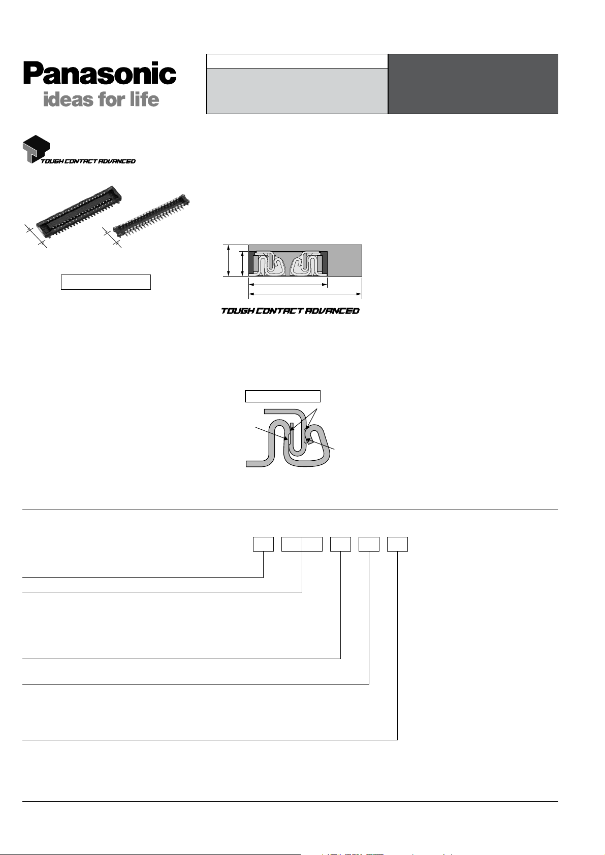
AXE5, 6
For board-to-FPC
2.5mm
Socket Header
2.0mm
RoHS compliant
Narrow pitch connectors
(0.4mm pitch)
FEATURES
1. 2.5 mm wide slim two-piece style
connectors
Compact and slim structure contributes
overall miniaturization of product design.
<Compared to F4S series (40 pin
contacts, when mated)>
• Width: 30% down
• Footprint: 30% down
F4S
1.0
0.8
2. “ ”
ensures high resistance to various
environments in lieu of slim and low
profile body
3. Simple lock structure provides
tactile feedback to ensure excellent
mating/unmating operation feel.
A4S
2.5
3.6
A4S Series
4. Mated heights of 0.8 and 1.0 mm are
available for the same foot pattern.
5. Connectors for inspection available
APPLICATIONS
Recommended for board-to-FPC
connections of mobile equipment,
such as cellular phones, smart
phones, laptops, and portable music
players
Simple lock structure
Simple lock
The connector gives the tactile feedback
when inserted, allowing reliable mating.
ORDERING INFORMATION
AXE 2 4
5: Narrow Pitch Connector A4S (0.4 mm pitch) Socket
6: Narrow Pitch Connector A4S (0.4 mm pitch) Header
Number of pins (2 digits)
Mated height
<Socket>
1: For mated height 0.8/1.0 mm
<Header>
1: For mated height 0.8 mm
2: For mated height 1.0 mm
Functions
2: Without positioning bosses
Surface treatment (Contact portion / Terminal portion)
<Socket>
4: Ni plating on base, Au plating on surface (for Ni barrier available)
<Header>
4: Ni plating on base, Au plating on surface
Double contact
V-notch
Panasonic Corporation Automation Controls Business Unit industrial.panasonic.com/ac/e
ACCTB7E 201201-T
Page 2
AXE5, 6
PRODUCT TYPES
Mated height Number of pins
10 AXE510124 AXE610124
12 AXE512124 AXE612124
14 AXE514124 AXE614124
16 AXE516124 AXE616124
18 AXE518124 AXE618124
20 AXE520124 AXE620124
22 AXE522124 AXE622124
24 AXE524124 AXE624124
26 AXE526124 AXE626124
28 AXE528124 AXE628124
30 AXE530124 AXE630124
0.8mm
1.0mm
Notes: 1. Order unit:
For volume production: 1-inner carton (1-reel) units
Samples for mounting check: 50-connector units. Please contact our sales office.
Samples: Small lot orders are possible. Please contact our sales office.
2. The above part numbers are for connectors without positioning bosses, which are standard. When ordering connectors with positioning bosses, please contact our
sales office.
3. Please contact us for connectors having a number of pins other than those listed above.
32 AXE532124 AXE632124
34 AXE534124 AXE634124
36 AXE536124 AXE636124
38 AXE538124 AXE638124
40 AXE540124 AXE640124
44 AXE544124 AXE644124
50 AXE550124 AXE650124
54 AXE554124 AXE654124
56 AXE556124 AXE656124
60 AXE560124 AXE660124
64 AXE564124 AXE664124
70 AXE570124 AXE670124
80 AXE580124 AXE680124
10 AXE510124 AXE610224
12 AXE512124 AXE612224
14 AXE514124 AXE614224
20 AXE520124 AXE620224
24 AXE524124 AXE624224
26 AXE526124 AXE626224
30 AXE530124 AXE630224
32 AXE532124 AXE632224
40 AXE540124 AXE640224
44 AXE544124 AXE644224
50 AXE550124 AXE650224
54 AXE554124 AXE654224
60 AXE560124 AXE660224
70 AXE570124 AXE670224
80 AXE580124 AXE680224
Socket Header Inner carton (1-reel) Outer carton
Part number Packing
5,000 pieces 10,000 pieces
ACCTB7E 201201-T
Panasonic Corporation Automation Controls Business Unit industrial.panasonic.com/ac/e
Page 3
AXE5, 6
SPECIFICATIONS
Characteristics
Item Specifications Conditions
Rated current 0.3A/pin contact (Max. 5 A at total pin contacts)
Rated voltage 60V AC/DC
Electrical
characteristics
Mechanical
characteristics
Environmental
characteristics
Lifetime
characteristics
Unit weight 20 pin contact type: Socket: 0.02 g Header: 0.01 g
Material and surface treatment
Part name Material Surface treatment
Molded
portion
Contact and
Post
Breakdown voltage 150V AC for 1 min.
Insulation resistance Min. 1,000MΩ (initial) Using 250V DC megger (applied for 1 min.)
Contact resistance Max. 90mΩ
Composite insertion force Max. 1.200N/pin contacts × pin contacts (initial)
Composite removal force Min. 0.165N/pin contacts × pin contacts
Contact holding force
(Socket contact)
Ambient temperature –55°C to +85°C No freezing at low temperatures. No dew condensation.
Soldering heat resistance
Storage temperature
Thermal shock resistance
(header and socket mated)
Humidity resistance
(header and socket mated)
Saltwater spray resistance
(header and socket mated)
H2S resistance
(header and socket mated)
Insertion and removal life 30 times
LCP resin
(UL94V-0)
Copper alloy
—
Contact portion:
Te r minal portion: Base: Ni plating Surface: Au plating (except the terminal tips)
The socket terminals close to the portion to be soldered have nickel barriers (exposed nickel portions).
Soldering terminals: Sockets: Base: Ni plating Surface: Pd+Au flash plating (except the terminal tips)
Min. 0.20N/pin contacts
Peak temperature: 260°C or less (on the surface of
the PC board around the connector terminals)
300°C within 5 sec. 350°C within 3 sec. Soldering iron
–55°C to +85°C (product only)
–40°C to +50°C (emboss packing)
5 cycles,
insulation resistance min. 100MΩ,
contact resistance max. 90mΩ
120 hours,
insulation resistance min. 100MΩ,
contact resistance max. 90mΩ
24 hours,
insulation resistance min. 100MΩ,
contact resistance max. 90mΩ
48 hours,
contact resistance max. 90mΩ
Base: Ni plating Surface: Au plating
Headers: Base: Ni plating Surface: Au plating (except the terminal tips)
No short-circuiting or damage at a detection current of 1 mA
when the specified voltage is applied for one minute.
Based on the contact resistance measurement method
specified by JIS C 5402.
Measuring the maximum force.
As the contact is axially pull out.
Infrared reflow soldering
No freezing at low temperatures. No dew condensation.
Sequence
0
1. –55 °C, 30 minutes
−3
2. ~ , Max. 5 minutes
+3
3. 85 °C, 30 minutes
0
4. ~ , Max. 5 minutes
Bath temperature 40±2°C,
humidity 90 to 95% R.H.
Bath temperature 35±2°C,
saltwater concentration 5±1%
Bath temperature 40±2°C, gas concentration 3±1 ppm,
humidity 75 to 80% R.H.
Repeated insertion and removal speed of max. 200 times/
hours
Panasonic Corporation Automation Controls Business Unit industrial.panasonic.com/ac/e
ACCTB7E 201201-T
Page 4

AXE5, 6
DIMENSIONS (Unit: mm)
The CAD data of the products with a CAD Data mark can be downloaded from: http://industrial.panasonic.com/ac/e
Socket (Mated height: 0.8 mm/1.0 mm)
CAD Data
A
B±0.1
0.40±0.05
0.15±0.03
0.70 (Suction face)
Y note
Z note
Note: Since the soldering terminals has a single-piece construction,
sections Y and Z are electrically connected.
0.30±0.03
C±0.1
(0.90)
0.77
2.20
2.50
1.06
General tolerance: ±0.2
Te rminal coplanarity
0.08
(Contact and
soldering terminals)
2.50
1.72
(0.39)
Dimension table (mm)
Number of pins/
dimension
10 4.5 1.6 3.4
12 4.9 2.0 3.8
14 5.3 2.4 4.2
16 5.7 2.8 4.6
18 6.1 3.2 5.0
20 6.5 3.6 5.4
22 6.9 4.0 5.8
24 7.3 4.4 6.2
26 7.7 4.8 6.6
28 8.1 5.2 7.0
30 8.5 5.6 7.4
32 8.9 6.0 7.8
34 9.3 6.4 8.2
36 9.7 6.8 8.6
38 10.1 7.2 9.0
40 10.5 7.6 9.4
44 11.3 8.4 10.2
50 12.5 9.6 11.4
54 13.3 10.4 12.2
56 13.7 10.8 12.6
60 14.5 11.6 13.4
64 15.3 12.4 14.2
70 16.5 13.6 15.4
80 18.5 15.6 17.4
A B C
Header (Mated height: 0.8 mm)
CAD Data
Soldering terminals
0.70 (Suction face)
0.40±0.05
0.15±0.03
0.15±0.03
A
B±0.1
C±0.1
0.65
1.42
0.84
1.46
Soldering terminals
(0.31)
General tolerance: ±0.2
Te rminal coplanarity
0.08
(Post and
soldering terminals)
2.00
1.28
(0.36)
Dimension table (mm)
Number of pins/
dimension
10 3.8 1.6 3.2
12 4.2 2.0 3.6
14 4.6 2.4 4.0
16 5.0 2.8 4.4
18 5.4 3.2 4.8
20 5.8 3.6 5.2
22 6.2 4.0 5.6
24 6.6 4.4 6.0
26 7.0 4.8 6.4
28 7.4 5.2 6.8
30 7.8 5.6 7.2
32 8.2 6.0 7.6
34 8.6 6.4 8.0
36 9.0 6.8 8.4
38 9.4 7.2 8.8
40 9.8 7.6 9.2
44 10.6 8.4 10.0
50 11.8 9.6 11.2
54 12.6 10.4 12.0
56 13.0 10.8 12.4
60 13.8 11.6 13.2
64 14.6 12.4 14.0
70 15.8 13.6 15.2
80 17.8 15.6 17.2
A B C
ACCTB7E 201201-T
Panasonic Corporation Automation Controls Business Unit industrial.panasonic.com/ac/e
Page 5

AXE5, 6
Header (Mated height: 1.0 mm)
Soldering terminals
Socket and Header are mated
Header
0.80±0.1
Socket
0.70 (Suction face)
Header
Socket
0.40±0.05
0.15±0.03
0.15±0.03
1.00±0.1
A
B±0.1
C±0.1
0.85
1.42
0.84
1.46
(0.31)
Soldering terminals
General tolerance: ±0.2
Te rminal coplanarity
0.08
(Post and
soldering terminals)
2.00
1.28
(0.36)
Dimension table (mm)
Number of pins/
dimension
10 3.8 1.6 3.2
12 4.2 2.0 3.6
14 4.6 2.4 4.0
20 5.8 3.6 5.2
24 6.6 4.4 6.0
26 7.0 4.8 6.4
30 7.8 5.6 7.2
32 8.2 6.0 7.6
40 9.8 7.6 9.2
44 10.6 8.4 10.0
50 11.8 9.6 11.2
54 12.6 10.4 12.0
60 13.8 11.6 13.2
70 15.8 13.6 15.2
80 17.8 15.6 17.2
A B C
EMBOSSED TAPE DIMENSIONS (Unit: mm) (Common for respective contact types, sockets and headers)
Specifications for taping
(In accordance with JIS C 0806-1990. However, not applied to
the mounting-hole pitch of some connectors.)
Tape I Tape II
(A±0.3)
(B)
(C)
(1.75)
8.0 (2.0) (4.0)
1.5 dia.
+0.1
0
Leading direction after packaging
(A±0.3)
(C)
(1.75)
8.0 (2.0) (4.0)
1.5 dia.
+0.1
0
Dimension table (Unit: mm)
Type/Mated height Number of pins Type of taping A B C D Quantity per reel
Common for sockets
and headers
0.8 mm/1.0 mm
24 or less Tape I 16.0 — 7.5 17.4 5,000
26 to 70 Tape I 24.0 — 11.5 25.4 5,000
80 Tape II 32.0 28.4 14.2 33.4 5,000
Connector orientation with respect to embossed tape feeding direction
Direction
of tape progress
Type
Socket Header
Specifications for the plastic reel
(In accordance with EIAJ ET-7200B.)
(D±1)
Top cover tape
Embossed carrier tape
380 dia.
Embossed mounting-hole
Taping reel
Common for A4S
Note: There is no indication on this product regarding top-bottom or left-right orientation.
Panasonic Corporation Automation Controls Business Unit industrial.panasonic.com/ac/e
ACCTB7E 201201-T
Page 6

For board-to-FPC
Connectors for
inspection usage
(0.4mm pitch)
AXE5, 6
A4S Series
FEATURES
1. 3,000 mating and unmating cycles
2. Same external dimensions and foot
APPLICATIONS
Ideal for module unit inspection and
equipment assembly inspection
pattern as standard type.
3. Improved mating
2.5mm
Socket Header
2.0mm
Insertion and removal easy due to a
reduction in mating retention force. This
is made possible by a simple locking
structure design.
RoHS compliant
Note: Mating retention force cannot be
warranted.
TABLE OF PRODUCT TYPES
✩: Available for sale
Product name Number of pins
12 14 16 18 20 22 24 26 28 30 32 34 36 38 40 44 50 54 56 60 64 70 80
A4S
for inspection
Notes: 1. Please inquire about number of pins other than those shown above.
2. Please inquire with us regarding availability.
3. Please keep the minimum order quantities no less than 50 pieces per lot.
4. Please inquire if further information is needed.
10
✩ ✩✩✩✩✩✩✩✩✩✩✩✩✩✩✩✩✩✩✩✩✩✩✩
PRODUCT TYPES
Specifications Par t No. Specifications Part No.
Socket Without positioning bosses AXE5E∗∗26 Header Without positioning bosses AXE6E∗∗26
Note: When placing an order, substitute the “∗” (asterisk) in the above part number with the number of pins for the specific connector.
NOTES
Recommended PC board and metal
mask patterns
Connectors are mounted with high pitch
density, intervals of 0.35 mm, 0.4 mm or
0.5 mm.
In order to reduce solder bridges and
other issues make sure the proper levels
of solder is used.
The figures to the right are recommended
metal mask patterns. Please use them as
a reference.
• Socket (Mated height: 0.8mm/1.0mm)
Recommended PC board pattern (TOP VIEW)
0.40±0.03
1.06±0.03
2.90±0.03
Recommended metal mask opening pattern
1.06±0.01
2.90±0.01
0.23±0.03
(0.92)
C 0.30
0.90±0.03
1.45±0.03
Metal mask thickness: When 120µm
(Terminal opening ratio: 70%)
(Metal-part opening ratio: 100%)
0.40±0.01
0.20±0.01
(0.92)
0.90±0.01
1.45±0.01
: Insulation area
(0.50)
(0.40)
C 0.30
0.20±0.03
2.00±0.01
1.90±0.03
2.80±0.01
• Header (Mated height: 0.8mm/1.0mm)
Recommended PC board pattern (TOP VIEW)
0.40±0.03
0.23±0.03
(0.65)
1.10±0.03
1.66±0.03
0.60±0.03
(0.53)
0.45±0.03
0.80±0.03
2.40±0.03
Recommended metal mask opening pattern
Metal mask thickness: When 120µm
(Terminal opening ratio: 70%)
(Metal-part opening ratio: 100%)
0.40±0.01
0.20±0.01
1.26±0.01
2.30±0.01
1.66±0.01
0.60±0.01
(0.53)
0.45±0.01
0.80±0.01
(0.52)
Please refer to the latest product
specifications when designing your
product.
ACCTB7E 201201-T
Panasonic Corporation Automation Controls Business Unit industrial.panasonic.com/ac/e
Page 7

NO TES FOR USING ADVANCED SERIES
NARROW -PITCH CONNECT ORS
Connector mounting
Excessive mounter chucking force may
deform the molded or metal part of the
connector. Consult us in advance if
chucking is to be applied.
Soldering
1) Manual soldering.
• Due to the connector’s low profile, if an
excessive amount of solder is applied
during manual soldering, the solder may
creep up near the contact points, or
solder interference may cause imperfect
contact.
• Make sure that the soldering iron tip is
heated within the temperature and time
limits indicated in the specifications.
• Flux from the solder wire may adhere to
the contact surfaces during soldering
operations. After soldering, carefully
check the contact surfaces and clean off
any flux before use.
• Be aware that a load applied to the
connector terminals while soldering may
displace the contact.
• Thoroughly clean the iron tip.
2) Reflow soldering
• Screen-printing is recommended for
printing paste solder.
• To determine the relationship between
the screen opening area and the PCboard foot pattern area, refer to the
diagrams in the recommended patterns
for PC boards and metal masks. Make
sure to use the terminal tip as a reference
position when setting. A v oid an excessiv e
amount of solder from being applied,
otherwise, interference by the solder will
cause an imperfect contact.
Terminal
Paste
solder
PC board
foot pattern
• Consult us when using a screen-printing
thickness other than that recommended.
• Depending on the size of the connector
being used, self alignment may not be
possible. Accordingly, carefully position
the terminal with the PC board pattern.
• The recommended reflow temperature
profile is given in the figure below
Recommended reflow temperature profile
Upper limit (Soldering heat resistance)
Temperature
Lower limit (Solder wettability)
260°C
230°C
180°C
150°C
Preheating
60 to 120 sec.
Peak temperature
220°C
200°C
25 sec.
70 sec.
Time
• The temperature is measured on the
surface of the PC board near the
connector terminal.
• Some solder and flux types may cause
serious solder creeping. Solder and flux
characteristics should be taken into
consideration when setting the reflow
soldering conditions.
• When performing reflow soldering on
the back of the PC board after reflow
soldering the connector, secure the
connector using, for example, an
adhesive (Double reflow soldering on the
same side is possible)
3) Reworking on a soldered portion
• Finish reworking in one operation.
• For reworking of the solder bridge, use
a soldering iron with a flat tip. Do not add
flux, otherwise, the flux may creep to the
contact parts.
• Use a soldering iron whose tip
temperature is within the temperature
range specified in the specifications.
Do not drop or handle the
connector carelessly. Otherwise, the
terminals may become deformed due
to excessive force or applied
solderability may be degraded during
reflow.
Do not insert or remove the
connector when it is not soldered.
Forcibly applied external pressure on
the terminals can weaken the
adherence of the terminals to the
molded part or cause the terminals to
lose their evenness.
Excessive prying-force applied to
one end may cause product breakage
and separation of the solder joints at
the terminal.
When removing the connector, be
sure not to tilt the connector
exceeding 15 degrees widthwise.
Excessive force applied for insertion
in a pivot action as shown may also
cause product breakage.
Align the header and socket positions
before connecting them.
or less
15 degrees
When cutting or bending the PC
board after mounting the connector,
be careful that the soldered sections
are subjected to excessive forces.
The soldered areas should not be subjected to forces.
Notes when using a FPC.
• When the connector is soldered to an
FPC board, during insertion and removal
forces may be applied to the terminals
and cause the soldering to come off. It is
recommended to use a reinforcement
board on the backside of the FPC board
to which the connector is being
connected. Mak e sure that the reinforcing
plate is larger than the outline of the
recommended PC board pattern (Outline
+ approx. 1 mm). The reinforcing plate is
made of SUS, glass epoxy or polyimide
that is 0.2 to 0.3 mm thick.
This connector employs a simple locking
structure. However, the connector may
come off depending on the size and
weight of the FPC, layout and reaction
force of FPC, or by drop impact. Make
sure to fully check the equipment’s
condition. To prevent any problem with
loose connectors, adopt measures to
prevent the connector from coming off
inside the equipment.
Other Notes
When coating the PC board after
soldering the connector (to prevent the
deterioration of insulation), perform the
coating in such a way so that the coating
does not get on the connector.
The connectors are not meant to be used
for switching.
Please refer to the latest product
specifications when designing your
product.
(Common)
ACCTB11E 201201-T
Panasonic Corporation Automation Controls Business Unit industrial.panasonic.com/ac/e
 Loading...