

Page 1
ORDER NO. OMTD040401C8
Personal Cellular Telephone
EB-A100
900 MHz 1800 MHz 1900 MHz
Tx Frequency Range: 880 - 915 MHz 1710 -1785 MHz 1850 -1990 MHz
Rx Frequency Range: 925 - 960 MHz 1805 -1880 MHz 1850 -1990 MHz
Tx / Rx separation 45 MHz 95 MHz 80 MHz
RF Channel Bandwidth 200 kHz
Number of RF channels 174 374 300
Speech coding Full rate / Enhanced Full rate
Operating temperature -10
Type Class 4 Handheld Class 1 Handheld Class 1 Handheld
RF Output Power 32 dBm maximum 29 dBm maximum 29 dBm maximum
Modulation GMSK
WAP / GPRS WAP 2.0 / GPRS class 8
Connection 8 ch / TDMA
Voice digitizing 13 kbps RPE-LTP / 13 kps ACLEP
Transmission speed 270.833 kbps
Signal Reception Direct conversion
Antenna Impedance
(External Connector)
Dimensions Height : 77 mm
(Excluding antenna)
Weight 66
Main Display LCD : 112 x 64 pixels
Illumination 2 LEDs for LCD Backlighting (White)
Keys 18-key Keypad, 2-way Navigation key
SIM 3 V Plug-in type only
External DC Supply 3.8 V
Voltage
Battery Standard Li-Ion 720mAh
Standby Time 78.3 - 230 hrs (
Talk Time 1.6 - 8.0 hrs (
(
∗
) The network being used, SIM card usage, and the condition of the battery affect Battery life.
°
C to +55 °C
50
Ω
Width : 44 mm
Depth : 17.8 mm
g
(including battery)
6 LEDs for Keypad Backlighting (Blue)
∗
)
∗
)
WARNING
This service information is designed for experienced repair technicians only and is not designed for use by the general public.
It does not contain warnings or cautions to advise non-technical individuals of potential dangers in attempting to service a
product.
Products powered by electricity should be serviced or repaired only by experienced professional technicians. Any attempt to
service or repair the product or products dealt with in this service information by anyone else could result in serious injury or
death.
2004 Panasonic Mobile Communications Co., Ltd.
All rights reserved. Unauthorized copying and
R
distribution is a violation of law.
Page 2

COMPANY LIABILITY
Every care has been taken to ensure that the contents of this manual give an accurate representation of the equipment.
However, Panasonic Mobile Communications Co., Ltd. accepts no responsibility for inaccuracies which may occur and reserves
the right to make changes to the specification or design without prior notice. The information contained in this manual and all
rights in any design disclosed therein, are and remain the exclusive property of Panasonic Mobile Communications Co., Ltd.
Other patents applying to material contained in this publication:
CP8 PATENTS
Comments or correspondence concerning this manual should be addressed to:
Panasonic Mobile Communications Co., Ltd.
600, Saedo-cho, Tsuzuki-ku, Yokohama, 224-8539, Japan
CONTENTS
1. INTRODUCTION . . . . . . . . . . . . . . . . . . . . . . . . . . . . . . . . . . . . . . . . . . . . . . . . . . . . . . . . . . . . . . . . . . . . . . . . . . . . . . . 1-1
1.1. Purpose of the Manual. . . . . . . . . . . . . . . . . . . . . . . . . . . . . . . . . . . . . . . . . . . . . . . . . . . . . . . . . . . . . . . . . . . . . . 1-1
1.2. Structure of the Manual . . . . . . . . . . . . . . . . . . . . . . . . . . . . . . . . . . . . . . . . . . . . . . . . . . . . . . . . . . . . . . . . . . . . . 1-1
1.3. Servicing Responsibilities . . . . . . . . . . . . . . . . . . . . . . . . . . . . . . . . . . . . . . . . . . . . . . . . . . . . . . . . . . . . . . . . . . . 1-1
2. GENERAL DESCRIPTION . . . . . . . . . . . . . . . . . . . . . . . . . . . . . . . . . . . . . . . . . . . . . . . . . . . . . . . . . . . . . . . . . . . . . . . 2-1
2.1. General . . . . . . . . . . . . . . . . . . . . . . . . . . . . . . . . . . . . . . . . . . . . . . . . . . . . . . . . . . . . . . . . . . . . . . . . . . . . . . . . . 2-1
2.2. Features . . . . . . . . . . . . . . . . . . . . . . . . . . . . . . . . . . . . . . . . . . . . . . . . . . . . . . . . . . . . . . . . . . . . . . . . . . . . . . . . 2-1
2.3. Handportable Main Kits . . . . . . . . . . . . . . . . . . . . . . . . . . . . . . . . . . . . . . . . . . . . . . . . . . . . . . . . . . . . . . . . . . . . . 2-1
3. OPERATING INSTRUCTIONS . . . . . . . . . . . . . . . . . . . . . . . . . . . . . . . . . . . . . . . . . . . . . . . . . . . . . . . . . . . . . . . . . . . . 3-1
3.1. General . . . . . . . . . . . . . . . . . . . . . . . . . . . . . . . . . . . . . . . . . . . . . . . . . . . . . . . . . . . . . . . . . . . . . . . . . . . . . . . . . 3-1
3.2. Liquid Crystal Display . . . . . . . . . . . . . . . . . . . . . . . . . . . . . . . . . . . . . . . . . . . . . . . . . . . . . . . . . . . . . . . . . . . . . . 3-1
3.3. Location of Controls . . . . . . . . . . . . . . . . . . . . . . . . . . . . . . . . . . . . . . . . . . . . . . . . . . . . . . . . . . . . . . . . . . . . . . . . 3-2
3.4. Concept of Operation . . . . . . . . . . . . . . . . . . . . . . . . . . . . . . . . . . . . . . . . . . . . . . . . . . . . . . . . . . . . . . . . . . . . . . 3-3
3.5. Alpha Entry . . . . . . . . . . . . . . . . . . . . . . . . . . . . . . . . . . . . . . . . . . . . . . . . . . . . . . . . . . . . . . . . . . . . . . . . . . . . . . 3-4
3.5.1. Character Set / Key Assignments . . . . . . . . . . . . . . . . . . . . . . . . . . . . . . . . . . . . . . . . . . . . . . . . . . . . . . . 3-4
3.5.2. Editing Alpha Entry . . . . . . . . . . . . . . . . . . . . . . . . . . . . . . . . . . . . . . . . . . . . . . . . . . . . . . . . . . . . . . . . . . 3-5
3.6. Features Structure . . . . . . . . . . . . . . . . . . . . . . . . . . . . . . . . . . . . . . . . . . . . . . . . . . . . . . . . . . . . . . . . . . . . . . . . . 3-5
3.7. Incoming Call Line Identification (CLI) . . . . . . . . . . . . . . . . . . . . . . . . . . . . . . . . . . . . . . . . . . . . . . . . . . . . . . . . . 3-13
3.8. Public Man Machine Interface (MMI) . . . . . . . . . . . . . . . . . . . . . . . . . . . . . . . . . . . . . . . . . . . . . . . . . . . . . . . . . . 3-13
3.8.1. General . . . . . . . . . . . . . . . . . . . . . . . . . . . . . . . . . . . . . . . . . . . . . . . . . . . . . . . . . . . . . . . . . . . . . . . . . . 3-13
3.8.2. Reading the Phonebook Memory Location . . . . . . . . . . . . . . . . . . . . . . . . . . . . . . . . . . . . . . . . . . . . . . . 3-13
3.8.3. Presentation of IMEI . . . . . . . . . . . . . . . . . . . . . . . . . . . . . . . . . . . . . . . . . . . . . . . . . . . . . . . . . . . . . . . . 3-13
3.8.4. Security . . . . . . . . . . . . . . . . . . . . . . . . . . . . . . . . . . . . . . . . . . . . . . . . . . . . . . . . . . . . . . . . . . . . . . . . . . 3-13
3.8.5. Call Hold . . . . . . . . . . . . . . . . . . . . . . . . . . . . . . . . . . . . . . . . . . . . . . . . . . . . . . . . . . . . . . . . . . . . . . . . . 3-13
3.8.6. Call Waiting . . . . . . . . . . . . . . . . . . . . . . . . . . . . . . . . . . . . . . . . . . . . . . . . . . . . . . . . . . . . . . . . . . . . . . . 3-13
3.8.7. Call Line Identification . . . . . . . . . . . . . . . . . . . . . . . . . . . . . . . . . . . . . . . . . . . . . . . . . . . . . . . . . . . . . . . 3-14
3.8.8. Telecommunication Services used for Public MMI . . . . . . . . . . . . . . . . . . . . . . . . . . . . . . . . . . . . . . . . . 3-14
3.8.9. Dial Divert . . . . . . . . . . . . . . . . . . . . . . . . . . . . . . . . . . . . . . . . . . . . . . . . . . . . . . . . . . . . . . . . . . . . . . . . 3-15
3.8.10. Call Bar . . . . . . . . . . . . . . . . . . . . . . . . . . . . . . . . . . . . . . . . . . . . . . . . . . . . . . . . . . . . . . . . . . . . . . . . . . 3-15
3.9. Troubleshooting . . . . . . . . . . . . . . . . . . . . . . . . . . . . . . . . . . . . . . . . . . . . . . . . . . . . . . . . . . . . . . . . . . . . . . . . . . 3-16
3.10. Important Error Messages . . . . . . . . . . . . . . . . . . . . . . . . . . . . . . . . . . . . . . . . . . . . . . . . . . . . . . . . . . . . . . . . . . 3-17
3.11. Security Codes . . . . . . . . . . . . . . . . . . . . . . . . . . . . . . . . . . . . . . . . . . . . . . . . . . . . . . . . . . . . . . . . . . . . . . . . . . 3-17
3.12. Glossary of Terms . . . . . . . . . . . . . . . . . . . . . . . . . . . . . . . . . . . . . . . . . . . . . . . . . . . . . . . . . . . . . . . . . . . . . . . . 3-18
i
Page 3

4. TECHNICAL SPECIFICATIONS
4.1. Tx Characteristics . . . . . . . . . . . . . . . . . . . . . . . . . . . . . . . . . . . . . . . . . . . . . . . . . . . . . . . . . . . . . . . . . . . . . . . . . 4-1
4.1.1. Frequency Error . . . . . . . . . . . . . . . . . . . . . . . . . . . . . . . . . . . . . . . . . . . . . . . . . . . . . . . . . . . . . . . . . . . . .4-1
4.1.2. Modulation Phase Error . . . . . . . . . . . . . . . . . . . . . . . . . . . . . . . . . . . . . . . . . . . . . . . . . . . . . . . . . . . . . . . 4-1
4.1.3. Output RF Spectrum due to Modulation . . . . . . . . . . . . . . . . . . . . . . . . . . . . . . . . . . . . . . . . . . . . . . . . . . 4-1
4.1.4. Output RF Spectrum due to Switching Transients . . . . . . . . . . . . . . . . . . . . . . . . . . . . . . . . . . . . . . . . . . . 4-1
4.1.5. Spurious Emissions at Antenna Connector . . . . . . . . . . . . . . . . . . . . . . . . . . . . . . . . . . . . . . . . . . . . . . . . 4-2
4.1.6. Residual Peak Power . . . . . . . . . . . . . . . . . . . . . . . . . . . . . . . . . . . . . . . . . . . . . . . . . . . . . . . . . . . . . . . . .4-2
4.2. Rx Characteristics . . . . . . . . . . . . . . . . . . . . . . . . . . . . . . . . . . . . . . . . . . . . . . . . . . . . . . . . . . . . . . . . . . . . . . . . . 4-2
4.2.1. Sensitivity . . . . . . . . . . . . . . . . . . . . . . . . . . . . . . . . . . . . . . . . . . . . . . . . . . . . . . . . . . . . . . . . . . . . . . . . . .4-2
5. TECHNICAL DESCRIPTION . . . . . . . . . . . . . . . . . . . . . . . . . . . . . . . . . . . . . . . . . . . . . . . . . . . . . . . . . . . . . . . . . . . . . 5-1
5.1. RF Overview . . . . . . . . . . . . . . . . . . . . . . . . . . . . . . . . . . . . . . . . . . . . . . . . . . . . . . . . . . . . . . . . . . . . . . . . . . . . . 5-1
5.1.1. RF Block Diagram . . . . . . . . . . . . . . . . . . . . . . . . . . . . . . . . . . . . . . . . . . . . . . . . . . . .. . . . . . . . . . . . . . . .5-1
5.1.2. RF Function Block . . . . . . . . . . . . . . . . . . . . . . . . . . . . . . . . . . . . . . . . . . . . . . . . . . . . . . . . . . . . . . . . . . . 5-2
5.1.3. Functional Description . . . . . . . . . . . . . . . . . . . . . . . . . . . . . . . . . . . . . . . . . . . . . . . . . . . . . . . . . . . . . . . . 5-3
5.2. Baseband Overview . . . . . . . . . . . . . . . . . . . . . . . . . . . . . . . . . . . . . . . . . . . . . . . . . . . . . . . . . . . . . . . . . . . . . . . 5-6
5.2.1. Introduction . . . . . . . . . . . . . . . . . . . . . . . . . . . . . . . . . . . . . . . . . . . . . . . . . . . . . . . . . . . . . . . . . . . . . . . . 5-6
5.2.2. Digital Baseband Processor . . . . . . . . . . . . . . . . . . . . . . . . . . . . . . . . . . . . . . . . . . . . . . . . . . . . . . . . . . . 5-7
5.2.3. Keypad . . . . . . . . . . . . . . . . . . . . . . . . . . . . . . . . . . . . . . . . . . . . . . . . . . . . . . . . . . . . . . . . . . . . . . . . . . . 5-8
5.3.4. Subscriber Identity Module (SIM) . . . . . . . . . . . . . . . . . . . . . . . . . . . . . . . . . . . . . . . . . . . . . . . . . . . . . . . 5-8
5.3.5. CPU Memory . . . . . . . . . . . . . . . . . . . . . . . . . . . . . . . . . . . . . . . . . . . . . . . . . . . . . . . . . . . . . . . . . . . . . . . 5-9
5.3.6. LCD . . . . . . . . . . . . . . . . . . . . . . . . . . . . . . . . . . . . . . . . . . . . . . . . . . . . . . . . . . . . . . . . . . . . . . . . . . . . . . 5-9
5.3.7. Real Tim Clock (RTC) . . . . . . . . . . . . . . . . . . . . . . . . . . . . . . . . . . . . . . . . . . . . . . . . . . . . . . . . . . . . . . . . 5-9
5.3. Audio System . . . . . . . . . . . . . . . . . . . . . . . . . . . . . . . . . . . . . . . . . . . . . . . . . . . . . . . . . . . . . . . . . . . . . . . . . . . 5-10
5.3.1. Voiceband Baseband Codec . . . . . . . . . . . . . . . . . . . . . . . . . . . . . . . . . . . . . . . . . . . . . . . . . . . . . . . . . . 5-10
5.3.2. Microphone . . . . . . . . . . . . . . . . . . . . . . . . . . . . . . . . . . . . . . . . . . . . . . . . . . . . . . . . . . . . . . . . . . . . . . . 5-11
5.3.3. Receiver . . . . . . . . . . . . . . . . . . . . . . . . . . . . . . . . . . . . . . . . . . . . . . . . . . . . . . . . . . . . . . . . . . . . . . . . . 5-12
5.3.4. Loud Speaker . . . . . . . . . . . . . . . . . . . . . . . . . . . . . . . . . . . . . . . . . . . . . . . . . . . . . . . . . . . . . . . . . . . . . 5-12
5.4. Power Management Subsystem . . . . . . . . . . . . . . . . . . . . . . . . . . . . . . . . . . . . . . . . . . . . . . . . . . . . . . . . . . . . . 5-13
5.4.1. Power Source . . . . . . . . . . . . . . . . . . . . . . . . . . . . . . . . . . . . . . . . . . . . . . . . . . . . . . . . . . . . . . . . . . . . . 5-13
5.4.2. Regulator Control . . . . . . . . . . . . . . . . . . . . . . . . . . . . . . . . . . . . . . . . . . . . . . . . . . . . . . . . . . . . . . . . . . 5-13
5.4.3. Voltage Regulation . . . . . . . . . . . . . . . . . . . . . . . . . . . . . . . . . . . . . . . . . . . . . . . . . . . . . . . . . . . . . . . . . 5-13
5.5. Battery Charging and Monitoring . . . . . . . . . . . . . . . . . . . . . . . . . . . . . . . . . . . . . . . . . . . . . . . . . . . . . . . . . . . . . 5-15
5.5.1. Charging Current . . . . . . . . . . . . . . . . . . . . . . . . . . . . . . . . . . . . . . . . . . . . . . . . . . . . . . . . . . . . . . . . . . . 5-15
5.5.2. Deeply Discharged Batteries . . . . . . . . . . . . . . . . . . . . . . . . . . . . . . . . . . . . . . . . . . . . . . . . . . . . . . . . . . 5-15
5.6. Test Point . . . . . . . . . . . . . . . . . . . . . . . . . . . . . . . . . . . . . . . . . . . . . . . . . . . . . . . . . . . . . . . . . . . . . . . . . . . . . . 5-16
5.6.1. Test Point Layout. . . . . . . . . . . . . . . . . . . . . . . . . . . . . . . . . . . . . . . . . . . . . . . . . . . . . . . . . . . . . . . . . . . 5-17
6. DISASSEMBLY / REASSEMBLY INSTRUCTIONS . . . . . . . . . . . . . . . . . . . . . . . . . . . . . . . . . . . . . . . . . . . . . . . . . 6-1
6.1. General . . . . . . . . . . . . . . . . . . . . . . . . . . . . . . . . . . . . . . . . . . . . . . . . . . . . . . . . . . . . . . . . . . . . . . . . . . . . . . . . . 6-1
6.1.1. Call Bar . . . . . . . . . . . . . . . . . . . . . . . . . . . . . . . . . . . . . . . . . . . . . . . . . . . .. . . . . . . . . . . . . . . . . . . . . . . 6-1
6.2. Disassembly . . . . . . . . . . . . . . . . . . . . . . . . . . . . . . . . . . . . . . . . . . . . . . . . . . . . . . . . . . . . . . . . . . . . . . . . . . . . . 6-2
6.3. Reassembly . . . . . . . . . . . . . . . . . . . . . . . . . . . . . . . . . . . . . . . . . . . . . . . . . . . . . . . . . . . . . . . . . . . . . . . . . . . . . . 6-5
7. REPAIR PROCEDURES . . . . . . . . . . . . . . . . . . . . . . . . . . . . . . . . . . . . . . . . . . . . . . . . . . . . . . . . . . . . . . . . . . . . . . . . . 7-1
7.1. Introduction . . . . . . . . . . . . . . . . . . . . . . . . . . . . . . . . . . . . . . . . . . . . . . . . . . . . . . . . . . . . . . . . . . . . . . . . . . . . . . 7-1
7.2. Lead Free (PbF) solder . . . . . . . . . . . . . . . . . . . . . . . . . . . . . . . . . . . . . . . . . . . . . . . . . . . . . . . . . . . . . . . . . . . . . 7-1
7.3. External Testing . . . . . . . . . . . . . . . . . . . . . . . . . . . . . . . . . . . . . . . . . . . . . . . . . . . . . . . . . . . . . . . . . . . . . . . . . . .7-1
7.3.1. General Information . . . . . . . . . . . . . . . . . . . . . . . . . . . . . . . . . . . . . . . . . . . . . . . . . . . .. . . . . . . . . . . . . . 7-1
7.4. Test Equipment Setup . . . . . . . . . . . . . . . . . . . . . . . . . . . . . . . . . . . . . . . . . . . . . . . . . . . . . . . . . . . . . . . . . . . . . . 7-4
7.4.1. Equipment Required . . . . . . . . . . . . . . . . . . . . . . . . . . . . . . . . . . . . . . . . . . . . . . . . . . . .. . . . . . . . . . . . . . 7-4
ii
Page 4

8. SOFTWARE DOWNLOAD & ADJUSTMENT PROCEDURE . . . . . . . . . . . . . . . . . . . . . . . . . . . . . . . . . . . . . . . . . . 8-1
8.1. Service Software Upgrade . . . . . . . . . . . . . . . . . . . . . . . . . . . . . . . . . . . . . . . . . . . . . . . . . . . . . . . . . . . . . . . . . . .8-1
8.2. MMI Test . . . . . . . . . . . . . . . . . . . . . . . . . . . . . . . . . . . . . . . . . . . . . . . . . . . . . . . . . . . . . . . . . . . . . . . . . . . . . . . . 8-3
8.3. Adjustment Procedure . . . . . . . . . . . . . . . . . . . . . . . . . . . . . . . . . . . . . . . . . . . . . . . . . . . . . . . . . . . . . . . . . . . . . . 8-4
8.3.1. Equipment Setting for TX/RX adjustment . . . . . . . . . . . . . . . . . . . . . . . . . . . . . . . . . . . . . . . . . . . . . . . . . 8-4
8.3.2. Main Subjects . . . . . . . . . . . . . . . . . . . . . . . . . . . . . . . . . . . . . . . . . . . . . . . . . . . . . . . . . . . . . . . . . . . . . . 8-4
8.3.3. Test Operation Procedure . . . . . . . . . . . . . . . . . . . . . . . . . . . . . . . . . . . . . . . . . . . . . . . . . . . . . . . . . . . . . 8-5
8.3.4. Enter Test . . . . . . . . . . . . . . . . . . . . . . . . . . . . . . . . . . . . . . . . . . . . . . . . . . . . . . . . . . . . . . . . . . . . . . . . . 8-5
8.3.5. TX Test . . . . . . . . . . . . . . . . . . . . . . . . . . . . . . . . . . . . . . . . . . . . . . . . . . . . . . . . . . . . . . . . . . . . . . . . . . . 8-6
8.3.6. RX Test . . . . . . . . . . . . . . . . . . . . . . . . . . . . . . . . . . . . . . . . . . . . . . . . . . . . . . . . . . . . . . . . . . . . . . . . . . . 8-9
8.3.7. Battery . . . . . . . . . . . . . . . . . . . . . . . . . . . . . . . . . . . . . . . . . . . . . . . . . . . . . . . . . . . . . . . . . . . . . . . . . . . 8-11
9. REPLACEMENT PARTS LIST . . . . . . . . . . . . . . . . . . . . . . . . . . . . . . . . . . . . . . . . . . . . . . . . . . . . . . . . . . . . . . . . . . . 9-1
9.1. Case and Cover Parts List . . . . . . . . . . . . . . . . . . . . . . . . . . . . . . . . . . . . . . . . . . . . . . . . . . . . . . . . . . . . . . . . . . 9-1
9.2. Main PCB . . . . . . . . . . . . . . . . . . . . . . . . . . . . . . . . . . . . . . . . . . . . . . . . . . . . . . . . . . . . . . . . . . . . . . . . . . . . . . . 9-2
10. BLOCK DIAGRAM . . . . . . . . . . . . . . . . . . . . . . . . . . . . . . . . . . . . . . . . . . . . . . . . . . . . . . . . . . . . . . . . . . . . . . . . . . . . 10-1
10.1. Baseband . . . . . . . . . . . . . . . . . . . . . . . . . . . . . . . . . . . . . . . . . . . . . . . . . . . . . . . . . . . . . . . . . . . . . . . . . . . . . . 10-1
10.2. RF Band . . . . . . . . . . . . . . . . . . . . . . . . . . . . . . . . . . . . . . . . . . . . . . . . . . . . . . . . . . . . . . . . . . . . . . . . . . . . . . . 10-2
11. CIRCUIT DIAGRAM . . . . . . . . . . . . . . . . . . . . . . . . . . . . . . . . . . . . . . . . . . . . . . . . . . . . . . . . . . . . . . . . . . . . . . . . . . . .11-1
11.1. Baseband . . . . . . . . . . . . . . . . . . . . . . . . . . . . . . . . . . . . . . . . . . . . . . . . . . . . . . . . . . . . . . . . . . . . . . . . . . . . . . .11-1
11.2. RF Band . . . . . . . . . . . . . . . . . . . . . . . . . . . . . . . . . . . . . . . . . . . . . . . . . . . . . . . . . . . . . . . . . . . . . . . . . . . . . . . .11-2
11.3. Analog Baseband . . . . . . . . . . . . . . . . . . . . . . . . . . . . . . . . . . . . . . . . . . . . . . . . . . . . . . . . . . . . . . . . . . . . . . . . .11-3
11.4. Others . . . . . . . . . . . . . . . . . . . . . . . . . . . . . . . . . . . . . . . . . . . . . . . . . . . . . . . . . . . . . . . . . . . . . . . . . . . . . . . . . .11-4
12. LAYOUT DIAGRAM . . . . . . . . . . . . . . . . . . . . . . . . . . . . . . . . . . . . . . . . . . . . . . . . . . . . . . . . . . . . . . . . . . . . . . . . . . . 12-1
12.1. Main PCB . . . . . . . . . . . . . . . . . . . . . . . . . . . . . . . . . . . . . . . . . . . . . . . . . . . . . . . . . . . . . . . . . . . . . . . . . . . . . . .12-1
iii
Page 5

1. INTRODUCTION
WARNING
The equipment described in this manual contains polarised capacitors utilising liquid electrolyte. These devices are entirely safe provided
that neither a short-circuit nor reverse polarity connection is made across the capacitor terminals. FAILURE TO OBSERVE THIS WARNING
COULD RESULT IN DAMAGE TO THE EQUIPMENT OR, AT WORST, POSSIBLE INJURY TO PERSONNEL RESULTING FROM
ELECTRIC SHOCK OR THE AFFECTED CAPACITOR EXPLODING. EXTREME CARE MUST BE EXERCISED AT ALL TIMES WHEN
HANDLING THESE DEVICES.
Caution
The equipment described in this manual contains electrostatic devices (ESDs). Damage can occur to these devices if the handling
procedures described in Section 4 are not adhered to.
Caution
This equipment may contain an internal battery in addition to the external battery packs. These batteries are recyclable and should be
disposed of in accordance with local legislation. They must not be incinerated, or disposed of as ordinary rubbish.
1.1. Purpose of the Manual
This Service Manual contains the information and procedures required for installing, operating and servicing the Panasonic
GSM Personal Cellular Mobile Telephone system operating on GSM Digital Cellular Networks.
1.2. Structure of the Manual
The manual is structured to provide service-engineering personnel with the following information and procedures:
1. General and technical information - provides a basic understanding of the equipment, kits and options, together with detailed
information for each of the major component parts.
2. Installation and operating information - provides instructions for unpacking, installing and operating the equipment.
3. Servicing information - provides complete instructions for the testing, disassembly, repair and reassembly of each major
component part. Step-by-step troubleshooting information is given to enable the isolation and identification of a malfunction,
and thus determine what corrective action should be taken. The test information enables verification of the integrity of the
equipment after any remedial action has been carried out.
4. Illustrated parts list - provided to enable the identification of all equipment components, for the ordering of spare /
replacement parts.
1.3. Servicing Responsibilities
The procedures described in this manual must be performed by qualified service engineering personnel, at an authorized
service centre.
The service engineering personnel are responsible for fault diagnosis and repair of all equipment described in this manual.
– 1-1 –
Page 6
2. GENERAL DESCRIPTION
2.1. General
This section provides a general description and kit composition details for the GSM Handportable Telephone System
and optional kits.
2.2. Features
The Panasonic Telephone Model A100 is a high performance, small, light, handset for business and
domestic use. The following features are provided:
■ Dual Codec, which includes Full Rate and Enhanced Full Rate (EFR) Speech Codec.
■ Triple Band, E-GSM 900 and PCS 1800 /1900 operation.
■ Tegic T9 Text Entry.
■ Voice Ringer.
■ Desktop handsfree function comprising integral echo cancellation and noise suppression.
■ Wireless Application Protocol (WAP) Browser.
■ Backup Battery.
■ Downloadable polyphonic melody ring tones.
■ Clock, Calculator and Currency Converter.
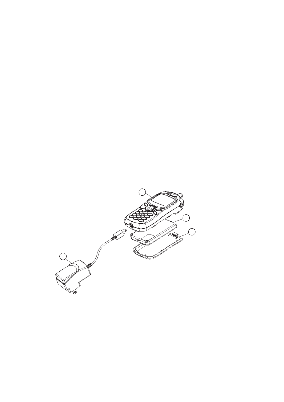
2.3. Handportable Main Kit
4
1
Main Unit
2
Battery
3
Battery Cover
Travel
Charger
Figure 2.1: Handportable Main Unit Kit Contents
– 2-1 –
Page 7
3. OPERATING INSTRUCTIONS
3.1. General
This section provides a brief guide to the operation and facilities available on the telephone handset.
Refer to the Operating Instructions supplied with the telephone for full operational information.
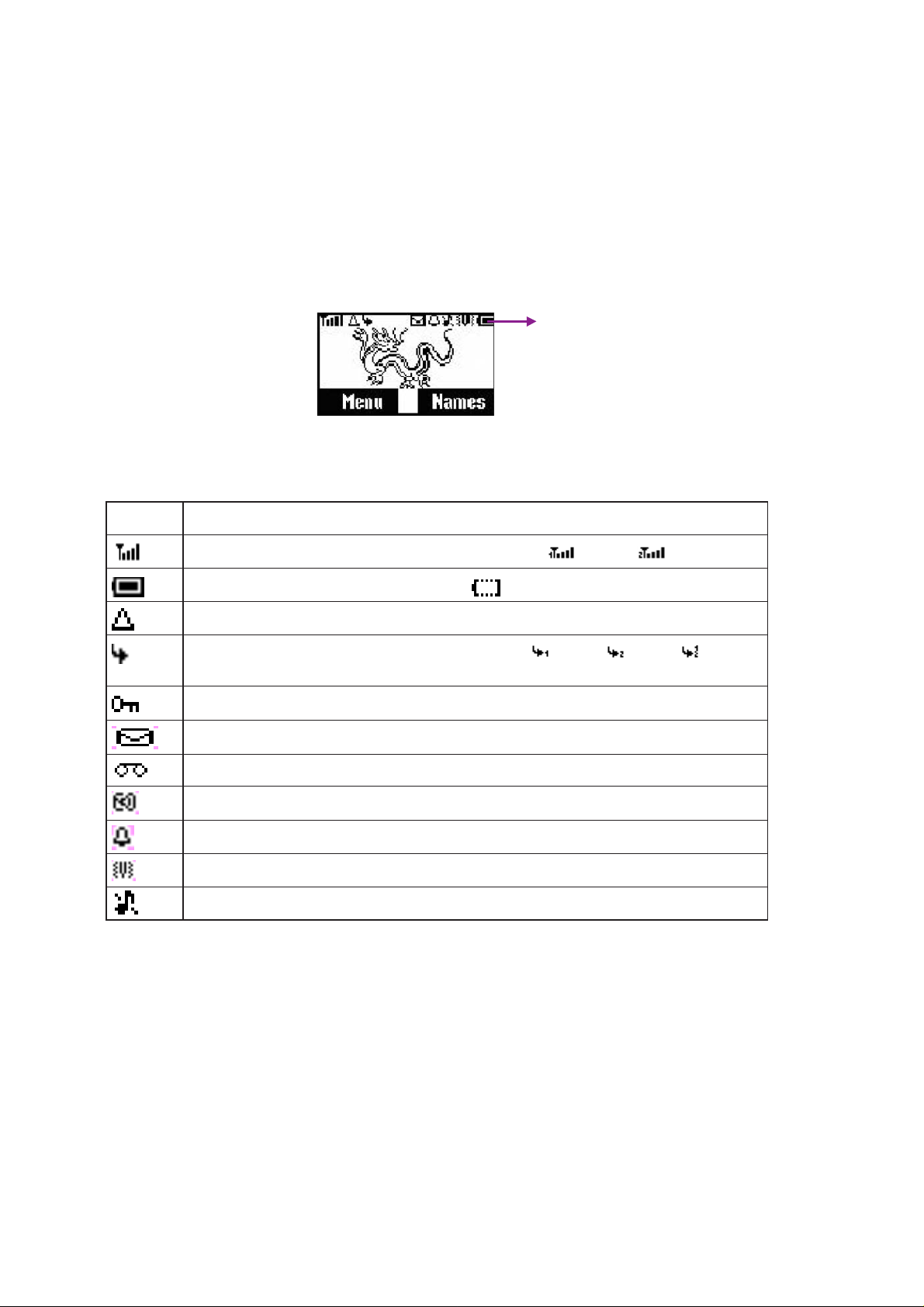
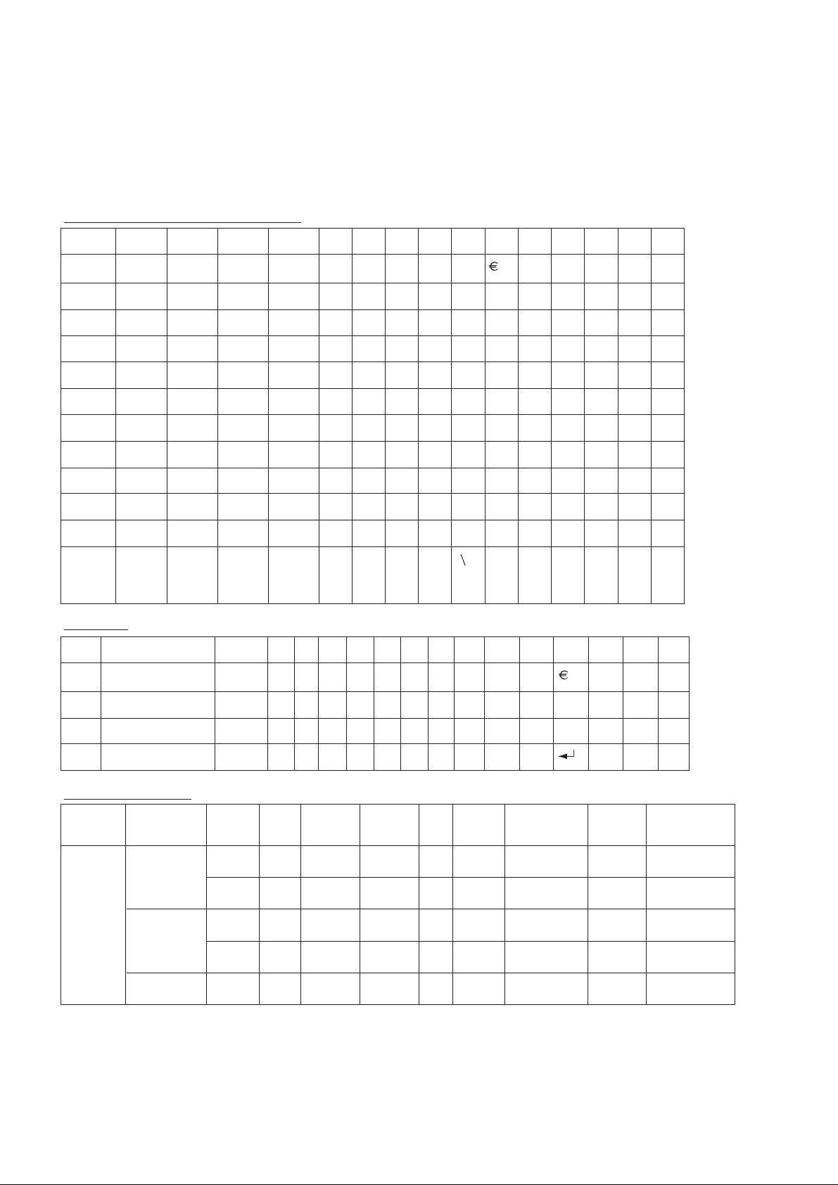
3.2. Liquid Crystal Display
The telephone handset has a graphical chip on glass display. The following icons are available:
Status Icons
Figure 3.1: Liquid Crystal Display
Icon Description
The received signal strength indication – No CHPS; : Line1; : Line2
Indicated the battery level / Low Battery:
Displayed when the user is registered to a non-home network-roaming
Displayed when call divert is enabled – No CPHS; : Line1; : Line2; : Line1 &
Line2
Displayed when phone lock is enabled
Displayed when an unread message is store or lights when message area is full
Voice mail indicator
Voice mail icon
Indicated alarm is set
Displayed when vibration alert is enable
Displayed when all tones or ring volume is off
– 3-1 –
Page 8
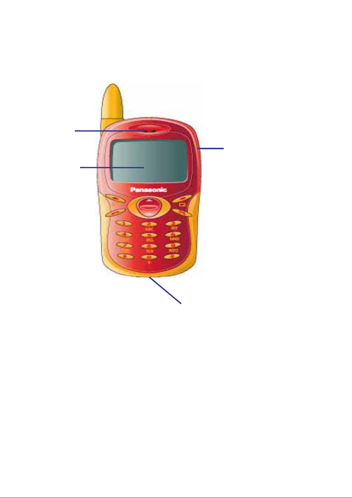
3.3. Location of Controls
Receiver
Display
Phone Jack
Charger Connection
The Phone Jack can be used as data transmission port to perform download and test tasks.
– 3-2 –
Page 9
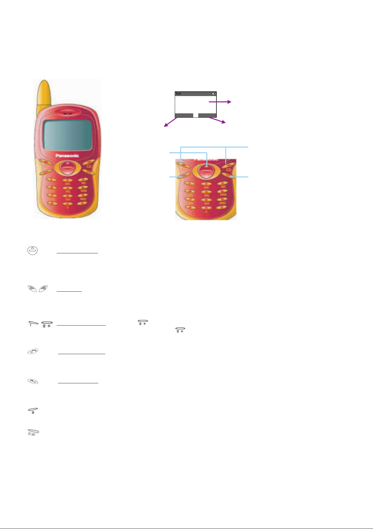
3.4. Concept of Operation
There is a close relationship between the Select keys, Navigation key and display.
Hello !
0
1 / 0 5 / 0 21 8 : 1 4
NamesMenu
Main Display
Right Hand SelectionLeft Hand Selection Area
Soft Key
Navigation key
Send and answer Key
Power / End Key
Navigation Key: Moving up and down through the options in the display area. In idle mode, pressing
to enter Own Menu. Own menu is a short cut to access your favourite menu. You can set it the personalize.
Soft keys: Perform the functions indicated by text shown on the LCD screen. In idle, long press left soft
key to enter Messages, long press right soft key to enter Profile Mode List.
Numeric key pads: Long Press to enter a "+" or "P". When you need to dial an extension number,
dial the phone number firstly then longer press to add a "P" and enter the extension number.
Send/Answer Key: Make a call or answer a call, In mode, check the last dialled list.
Power/End Key: To end a call return to idle mode, return to previous menu or reject an
incoming call, Long press it to switch the phone on/off.
In idle, long press to active Browser.
In idle, long press to switch the Mute Mode on and off.
– 3-3 –
Page 10
3.5. Alpha Entry
3.5.1. Character Set / Key Assignments
Alpha entry is used to enter alphanumeric characters in to the Phonebook, Short Message and Greeting
Message areas.
Alphabetic, small / capital letter mode :
Key 1. 2. 3. 4. 5. 6. 7. 8. 9. 10. 11. 12. 13. 14. 15.
11 / ( ) <=>%
22äà
a / A
d / D
33éè
4
g / G
j / J
55
66öñ
m / M
77ß
p / P
t / T
88üù
9z9æøå
w / W
∗∗ ΘΛΓ∆ ΞΠΣΦ
0 Space 0 . , ? ! + - : ¿ ¡ " ' ; _
#T9
on/off
mode
T9 mode :
Key 1. 2. 3. 4. 5. 6. 7. 8. 9. 10. 11. 12. 13. 14. 15. 16.
b / B
e / E
h / H
k / K
n / N
q / Q
u / U
x / X
Space # £ $ ¥ ¤ @
c / C
f / F
i / I
l /L
o / O
r / R s / S
v / V
y / Y
4ì
ç
ò
~
&
Ω
Ψ
§^I
1
1/()<>[]{%}~&
∗
∗ Γ∆ΘΛΞΠΣΦΨ Ω
Space .0?,!+-=:¿¡"';_
0
T9 on/off mode $£¥@¤Space # \ § ^ |
#
T9 Editor Sequence :
Key T9 Editor
Sequence
<Send>
• Key 1,2,3,4,5,6,7,8,9,0 long press provides corresponding numbers.
• All other keys are used for Tegic T9 intelligent text mapping.
• TC : Traditional Chinese; SC: Simplified Chinese; BPMF : Input method of traditional Chinese
• The thirteenth character of Key 0 only exits in SMS editor.
• The Thai multitap only exists when Thai language exist and the mapping switch on it.
TC
SC
Thai
Tegic
mode
T9 on
T9 off
T9 on
T9 off Abc abc ABC 123 BPMF
T9 off Abc abc ABC 123 Thai
1. 2. 3. 4. 5. 6.
T9
AbcT9abc
T9
AbcT9abc
T9
AbcT9abc
T9
ABC
T9
ABC
T9
ABC
123 BPMF
123 BPMF
123 BPMF
Stroke_TC
Stroke_TC
Stroke_TC
Stroke_TC
7.
PinYin
PinYin
PinYin
PinYin
8.
Stroke_TC
Stroke_TC
Stroke_TC
Stroke_TC
– 3-4 –
Page 11

3.5.2. Editing Alpha Entry
Pressing will move the cursor up or down one line. Pressing will move the cursor left or right one character.
When the cursor is moved over a character and another key pressed will insert the new character.
Pressing will delete the character to the left of the character.
3.6. Features Structure
Feature Set Listing
1 Telephone Functionality
Display and Lighting
LCD Display
Received Signal Strength Indication
Battery Status Icon
Call Processing Signal Indication
Dialled Number Indication
Last Dialed Digit Clear/Entire Line Clear
Own Telephone Number Indication
Service/No Service Indication
Country/PLMN Indication
Service Provider Indication
Roaming Indication
SMS Ariving Indication
SMS Overflow Indication
Vibration Mode Status Indication
Lock Status Indication (Keypad Lock)
Greeting Message Editing
PIN Greeting Animations
Power On/Off Animations
Clock Alarm Indication
Show Time & Date
Back-lighting
LCD Backlight
Keypad Backlight
Incoming Call Backlighting
– 3-5 –
Page 12

Security
Access Codes
PIN Check
Change PIN
FDN Mode (On/Off)
ME Personalization
Network Lock
Network Subset Lock
Service Provider Lock
Corporate Lock
SIM Lock
PIN
PUK
PIN2
PUK2
Phone Code
Multi Network Lock
Sound Settings
Ring Tone/Melody (15 Ringtones predefined, 5 editable)
Ring Volume Control (1-5)
Alert Type
Keypad Tone
Service Tone
Ring Only
Ring Once
Vibration Only
Vibration and Ring
None
On (Individual Key Sounds: DTMF tones)
Off (No Keypad Sound)
Network Found
Warning Tones (for low battery, etc.)
– 3-6 –
Page 13

Phone Parameters
Greeting Message
Own Number
Language
Any-key Answer (On/Off)
Auto Answer (On/Off)
Illumination (On/Off)
Redial
Reset Setting to Default
My Phonebook
Hot Key Dial (On/Off)
Clock Setting
Set Time
Set Date
Key 1 to 9 assigned to the Phone-number in SIM or ME records
from 1 to 9, press <Send> to dial out
Display Format
Languages/Fonts/Bitmaps
Fonts & Bitmaps
Character Set Definition, Mapping & Decoding
Text String Translation For all languages
Full GSM Character Set
Network Services (Requires Carrier Protocol Stack Support)
Call Diverting
Divert Always
Busy
No Reply
Unreachable
Cancel All
Call Barring
All outgoing Calls
Outgoing International Calls
Outgoing International Calls, Except Home
All Incoming Calls
All Incoming Calls When Roaming
Cancel All
Change barring Password
– 3-7 –
Page 14

Call Waiting
Enable
Disable
Network Selection
Network Select
Auto/Manual Selection
Preferred List
Band Select
Line Identification
Calling Line Identification Presented (CLIP)
Calling Line Identification Restricted (CLIR)
Connected Line Identification Restriction (COLP)
Connected Line Identification Restriction (COLR)
In-Call Menu (Requires Protocol Stack Support)
Call on Hold/Swap
Answer Second Call
Display of Change Advice Information
Multiple Call
Having Private Conversion With One Participant
Dropping One Participant
SMS (Requires Carrier and Stack Support)
UCS2, 8 Bit Encoding support
Read Message
Header Display
Message Number
Message Status
View Message
Sender's Phone Number (If Sent)
Date And Time Message Received
Message Text
EMS Picture Message
EMS Sound Message
Text Reply
Change SMS Center Number
Send Message
Save Message
– 3-8 –
Page 15

Delete Message
Extract Number From Message
Recognition of phone number
Send (Resend Message Already Sent)
Edit Message
Write Messages
Send
Insert Predefined Text
Insert Picture/Melody (EMS MO)
Save and Send Message
Save Only
Auto capital letter in the beginning of string input
Predefined Text (15)
Edit Preset Message
Clear Preset Message to Empty
Setup
Call Records
Service Center Number
Store SMS Center Number
Edit SMS Center Number
Message Type
Reply Path
Status Report
Validity Period
Broadcast
Read Messages
Save Messages
Receive (Enable/Disable)
Channel List (scan up to 5 channels in parallel)
Enter New Channel
All Channels (Enable/Disable)
Language Preference
Missed Calls (Number: 20)
Display Number, Name (if available), Date and Time
Edit, Dial or Save Number
Delete Number From List
– 3-9 –
Page 16

Received Calls (Number: 50)
Display Number, Name (if available), Date and Time
Edit, Dial or Save Number
Delete Number From List
Dialled Calls (Number: Minimum to 50)
Display Number, Name (if available)
Edit or Save Number
Redial Number
Delete Number
Call Time
Last Call Time
Total Sent
Total Received
Reset Times
Call Cost (Requires Protocol Stack Support)
Last Call Cost
Total Cost
Max Cost
Reset Counters
Set Max Cost
Price/Unit
GSM 2.30 Public MMI and GSM 2.90 USSD
2 Optional Network Service (Requires Carrier and Protocol Stack Support)
SIM Toolkit
Class 1 (SIM Content Update)
Class 2 (SMS Proactive SIM)
Class 3 Send USSD
– 3-10 –
Page 17
3 Applications
Phonebook
Phonebook Name and Number Storage
ADN (Depends on SIM, Max 255)
FDN (Number of entries Max 50)
Own Number
Service Dialling Number
Dialling From Phonebook
Phonebook Options
Edit Phonebook Number and Name
Erase Phonebook Number and Name
Speed Dialling (1-9)
Grouping (5)
- Friends
- Colleagues
- Family
- Others
- VIP
Calculator
Currency Converter
World Clock
Select time zone from 24 time zones.
Set Time
Set Date
Daylight Saving On/Off
Time Format
Date Format
Melody Composer (Max. 5)
Wall Paper in Idle Mode (10 Default; size: 112 x 40)
Melody Manager (15 default melody, 5 Composed)
Pre-View all downloaded and composed ring tones
Set to Ringer Tone
Games
Hitting Mouse
Memorize
– 3-11 –
Page 18

4 Miscellaneous
Battery Management
Accessory Support
Alpha-numeric Input
T9 Smart input version 5.0
Low Battery Warning
Power Off Indication
Charging Status
Alpha Mode
Numeric Mode
English: Predictive input
Chinese:
1. Bopomofo (for Traditional Chinese)
2. Pinyin (for Simplified Chinese)
3. Stroke Traditional Chinese
4. Stroke Simplified Chinese
– 3-12 –
Page 19

3.7. Incoming Call Line Identification (CLI)
When a call is received the last eight digits of the CLI information is matched with the phonebook
Therefore an incoming call could be matched to the wrong phonebook entry.
3.8. Public Man Machine Interface (MMI)
3.8.1. General
It is possible to operate all GSM telephones in the same way using the Public MMI. The following operations will work with all
GSM telephones. However, this information is restricted to those operations supported by the telephone.
The * and # in the following procedures should be replaced by and respectively. Also <SND> and <END> should be
replaced with and keys.
3.8.2. Reading the Phonebook Memory Location
# <MEMORY LOCATION>
Leading zeros can be left out of the location number, e.g. 007 can be 7.
3.8.3. Presentation of IMEI
* # 0 6 #
3.8.4. Security
Change PIN * * 0 4 * <OLD PIN> * <NEW PIN> * <NEW PIN> #
Change PIN2 * * 0 4 2 * <OLD PIN2> * <NEW PIN2> * <NEW PIN2> #
Unblock PIN * * 0 5 * <PIN UNBLOCKING KEY> * <NEW PIN> * <NEW PIN> #
Unblock PIN2 * * 0 5 * <PIN2 UNBLOCKING KEY> * <NEW PIN2> * <NEW PIN2> #
3.8.5. Call Hold
Place a Call on Hold 2 <SND>
Recall a Held Call 2 <SND>
Make a Second Call <TELEPHONE NUMBER>?<SND>
Swap between two Held Calls 2 <SND>
End Held Call 0 <SND>
End Active Call 1 <SND>
Reject Incoming Call 0 <SND>
3.8.6. Call Waiting
Enable Call Waiting *43 * <SND>
Disable Call Waiting #43 * <SND>
Call Waiting Status * # 4 3 * # <SND>
– 3-13 –
Page 20

3.8.7. Call Line Identification
Feature Service Code
Calling Line Identification Presentation (CLIP) 30
Calling Line Identification Restriction (CLIR) 31
Connected Line Presentation (CLOP) 76
Connected Line Restriction (CLOR) 77
Enable * <SERVICE CODE> * # (SND>
Disable # <SERVICE CODE> * # (SND>
Temporary Suppress Identification # 31 # <TELEPHONE NUMBER> <SND>
Temporary Display Identification * 31 # <TELEPHONE NUMBER> <SND>
3.8.8. Telecommunication Services used for Public MMI
Teleservice
Service MMI Service Code
All teleservices 10
Telephony 11
All data teleservices 12
Facsimile services 13
Short Message Service (SMS) 16
All teleservices except SMS 19
Voice group service 17
Bearer Service
Service MMI Service Code
All bearer services 20
All asynchronous services 21
All synchronous services 22
All data synchronous services 24
All data asynchronous services 25
All dedicated packet access 26
All dedicated PAD access 27
– 3-14 –
Page 21

3.8.9. Dial Divert
Call Divert Type Service Code
Divert all calls 21
Divert all calls if busy 67
Divert all calls if no reply 61
Divert if not reachable 62
Set Call Bar * * <SERVICE CODE> * <FORWARD TELEPHONE NUMBER> *
(Except "No Reply") <TELECOMMUNICATION SERVICE> # <SND>
Set "No Reply" Call Bar * * <SERVICE CODE> * <FORWARD TELEPHONE NUMBER> *
<TELECOM' SERVICE> * <TIME TO RING (sec)>#<SND>
Clear # # <SERVICE CODE> * <TELECOMMUNICATION SERVICE> * # <SND>
Status * * # <SERVICE CODE> * <TELECOMMUNICATION SERVICE> * # <SND>
Clear all Call Diverts # # 002 #
3.8.10. Call Bar
Call Bar Type Service Code
All outgoing calls 33
Outgoing International calls 331
Outgoing International calls except those to the PLMN 332
All incoming calls 35
Incoming international calls when roaming 351
Set * <PASSWORD> * <TELECOMMUNICATION SERVICE> # <SND>
Clear # <TELECOMMUNICATION SERVICE> # <SND>
Status # <TELECOMMUNICATION SERVICE> # <SND>
Clear all Call Bar Type # 330 * <PASSWORD> # <SND>
Change Call Bar * * 03 * * <OLD PASSWORD> * <NEW PASSWORD> * <NEW
Password PASSWORD # <SND>
– 3-15 –
Page 22
3.9. Troubleshooting
The user is given the following information and advised to contact the dealer if the problems persist:
Problem Cause Remedy
Telephone will not switch on Check that the battery pack is fully charged
and correctly connected to the telephone.
Extremely short battery life
for a new battery pack
Short battery life for an
old battery pack
The battery level indicator
does not light when
charging
Calls cannot be made
Calls cannot be made from
Fixed Dial Store
The network in use and the
condition of the battery pack can
affect battery life.
The battery pack was worn out. Replace with a new one.
If a battery is deeply discharged
it will take a short time before
there is sufficient power in the
telephone to light the battery
level indicator .
The telephone is locked. Unlock the telephone.
Outgoing calls are barred. Disable the outgoing call barring
The telephone is not registered
to a network.
Avoid areas of poor reception. Ensure
batteries fully charged.
Leave to charge for several minutes in
temperatures between +5 °C and +35 °C
(Phone Option: Security: Call bar).
Move to a coverage area and operate the
telephone after it has registered with a
network.
Check that SIM supports Fixed Dial
Check if the Fixed Dial is switched on
(Phone Operation: Security: Fixed Dial).
Check the telephone number is stored in the
Fixed Dial.
Calls cannot be received
Emergency calls cannot be
made
be recalled
The telephone is not switched
on.
Incoming calls are barred. Disable the incoming call barring (Phone
The telephone is not
registered to a network.
User's phone is not in a GSM
coverage area.
The telephone is locked. Unlock the telephone.Telephone numbers Cannot
Fixed Dial is switched on Switched off Fixed Dial
Switch the telephone on.
Option: Security: Call Bar).
Move to a coverage area and operate the
telephone after it has registered with a
network.
Check that the antenna symbol is
displayed. Move to a coverage area and
operate the telephone when the antenna
symbol is displayed.
(Phone Option: Security: Fixed Dial).
– 3-16 –
Page 23

3.10. Important Error Messages
The following table is a list of error messages that may occur during use of the telephone, with a
description and suggested course of action:
Error Message Explanation / Remedy
Area not Allowed Roaming in the selected area is not allowed.
Network not allowed Roaming with the selected network is not allowed.
Security Failure The network has detected authentication failure because the SIM is not registered with
that network. Contact the Service Provider.
SIM Blocked The SIM is blocked because the wrong PUK has been entered 10 times.
Contact the Service Provider.
SIM Error The telephone has detected a problem with the SIM. Switch the telephone off and then
back on. If the message does not disappear, contact the Service Provider.
Message Rejected
Store Full
PIN2 Invalidated The PIN2 is blocked permanently because the wrong PUK2 has been entered 10
Warning Store Full
Continue?
A message has been received but the message store is full. To receive messages,
delete some of the currently stored messages.
times. Services controlled by PIN2 cannot be used. Contact the Service Provider.
The message area is full. New messages cannot be stored unit some of the currently
stored messages are deleted.
3.11. Security Codes
Code Type Number or Digits Description
Personal Identification
Number (PIN)
PIN2 4 to 8 Controls memory security. Supplied by the service provider.
PIN/PIN2 Unblocking
Key
(PUK/PUK2) 8 Used to unblock PIN and PIN2. A PIN or PIN2 will become
4 to 8 Controls SIM security. Supplied by the service provider.
Supplied by the service provider.
blocked if the wrong PIN or PIN2 is entered three times.
When the blocked PIN or PIN2 is unblocked, a new PIN or
PIN2 must be entered.
If the wrong PUK or PUK2 is entered 10 times, the cursor
SIM will be unusable.
Password 4 Controls the call bar function. If the wrong password is
entered three times, this service will be revoked.
Supplied by the service provider.
Phone lock Code 4 to 8 Controls telephone security.
– 3-17 –
Page 24

3.12. Glossary of Terms
Term Definition
DTMF Dual Tone Multiple Frequency tones. The numeric keys 0 to 9, and * and # will generate
different DTMF tones when pressed during conversation. These are used to access
voice mail, paging and Home banking services.
GSM Global System for Mobile communications. The name given to the advanced digital
technology that the telephone uses.
Home network The GSM network on which subscription details are held.
Hot Key Dial Hot Key Dial allows quick access to numbers stored in the Phonebook of Service Dial
Number list. The source of the Hot Key Dial may be defined by the user or
preprogrammed by the Service Provide. It is most likely to be preprogrammed to the
Service Dial Numbers by the Service Provider.
Phone Lock code Used for security of the telephone.
Message Centre Where messages are sent before they are forwarded on to their destination. The
Message Centre telephone number may be programmed into the SIM or supplied by
the service provider.
Network operator The organization responsible for operating a GSM network.
Password Used for the control of the call bar function. Supplied by the service provider.
PIN Personal Identification Number used for SIM security. Supplied by the service provider.
PIN2 Personal Identification Number used for the control of Fixed Dial Memory and call
charge metering. Supplied by the service provider.
PUK / PUK2 PIN/PIN2 Unblocking Key. Used to unblock the PIN/PIN2. Supplied by the service
provider.
Registration The act of locking on to a GSM network. This is usually performed automatically by the
telephone.
Roaming The ability to use the telephone on networks other than the Home network.
Service Dial Service Dial Numbers are predefined numbers that allow the user to access a set of
Numbers special services provided by the Service Provider. For example billing information or
access to Voice Mail.
Service provider The organization responsible for providing access to the GSM network.
SIM Subscriber Identification Module. A small smart-card which stores unique subscriber
and user-entered information such as Phone Book, Fixed Dial Memory and short
messages. Supplied by the service provider.
Supplementary Network-controlled GSM functions supported by the telephone. Supplementary services
may only be available on a subscription bases.
Service Spaces in a stored telephone number. When the telephone number is recalled pressing
Wild numbers a numeric key will fill in a space. This can be used to restrict dialing to a specific area.
– 3-18 –
Page 25

4. TECHNICAL SPECIFICATIONS
4.1. Tx Characteristics
All data is applicable to E-GSM 900 and GSM 1800 except where stated.
4.1.1. Frequency Error
±0.1 ppm max., relative to base station frequency.
4.1.2 Modulation Phase Error
RMS: Equal to or less than 5 °
Peak: Equal to or less than 20 °
4.1.3. Output RF Spectrum due to Modulation
Offset from Centre Frequency (kHz)
±100 +0.5
±200 –30
±250 –33
±400 –60
±600 to 1800 –60
4.1.4. Output RF Spectrum due to Switching Transients
Offset from Centre Frequency (kHz)
±400 –19 –22 –22
±600 –21 –24 –24
±1200 –21 –24 –24
±1800 –24 –27 –27
Measurement conditions for output RF spectrum measurements:
Frequency Span 0 Hz
Measurement Bandwidth: 30 kHz
Video Bandwidth: 30 kHz (modulation)
100 kHz (switching)
Average (Modulation) Over 200 burst
Peak Hold (Switching) Over 10 burst
Maximum Level Relative to Carrier (dB)
Maximum Level (dBm)
E-GSM 900 GSM 1800
GSM 1900
– 4-1 –
Page 26

4.1.5. Spurious Emissions at Antenna Connector
Frequency Range
100 kHz to 50 MHz – 10 kHz 30 kHz –36 –36
50 MHz to 500 MHz – 100 kHz 300 kHz –36 –36
500 MHz to 1 GHz 0 to 1MHz
1 GHz to 12.75 GHz
Excl. relevant TX band
E-GSM : 880 MHz to 915 MHz
DCS : 1710 MHz to 1785 MHz
-and the Rx bands
925 MHz - 960 MHz
1805 MHz - 1880 MHz
Relevant TX band:
E-GSM : 880 MHz to 915 MHz
DCS :1710 MHz to 1785 MHz
Frequency
offset
0 to 10 MHz
> 10 MHz
> 30 MHz
(off trom edge
of relevant Tx band)
1.8 MHz to 6.0 MHz
> 6.0 MHz
Filter
Bandwidth
100 kHz 300KHz
100 kHz
300 kHz
3 MHz
30 kHz
100 kHz
Approx
Video B/W
300 kHz
1 MHz
3 MHz
100 kHz
300 kHz
E-GSM 900 GSM1800/1900
–36 –36
–30
–30
–30
–36
–36
4.1.6. Residual Peak Power
Equal to or less than 70 dBc (BW = 300 kHz)
4.2. Rx Characteristics
Limits(dBm)
–30 (1.0 GHz - 1.710 GHz)
–36 (1.710 GHz - 1.785GHz)
–30 (1.785 GHz - 12.75GHz)
–36
–36
4.2.1. Sensitivity
E-GSM 900 Full Rate Speech
The reference sensitivity performance in terms of frame erasure, bit error, or residual bit error rates (whichever is appropriate) is
specified in the following table, according to the propagation conditions.
The reference sensitivity level is < -102 dBm.
NOTE: 1 < α < 1.6. The value of α can be different for each channel condition but must remain the
same for FER and class 1b RBER measurements for the same channel condition.
Channels Propagation Conditions
TU high
TCH/FS FER
Class lb (RBER)
Class ll (RBER)
Tes t Limit
error rate
%
6.742*α
0.42/α
8.33
Minimum
No of
samples
8,900
1,000,000
120,000
Propagation Conditions
RA
Test Limit
error rate
7.5 24,000 9.33 60,000
%
Minimum
No of
samples
Propagation Conditions
HT
Test Limit
error rate
%
Minimum
No of
samples
Static Conditions
Test Limit
error rate
%
0.122*α
0.41/α
2.439
Minimum
No of
samples
164000
20,000,000
8,200
– 4-2 –
Page 27

GSM 1800/1900 Full Rate Speech
The reference sensitivity performance in terms of frame erasure, bit error, or residual bit error rates (whichever is appropriate)
is specified in the following table, according to the propagation conditions.
Channels Propagation Conditions
TU high
Test Limit
error rate
TCH/FS FER
Class lb (RBER)
Class ll (RBER)
The reference sensitivity level is < -102 dBm.
NOTE: 1 < α < 1.6. The value of α can be different for each channel condition but must remain the
same for FER and class 1b RBER measurements for the same channel condition.
4.478*α
0.32/α
8.333
%
Minimum
No of
samples
13400
1,500,000
60,000
Propagation Conditions RAPropagation Conditions
HT
Test Limit
error rate
7.5 24000 9.333 30000
%
Minimum
No of
samples
Test Limit
error rate
%
Minimum
No of
samples
Static Conditions
Test Limit
error rate
%
0.122*α
0.41/α
2.439
Minimum
No of
samples
164000
20,000,000
8200
– 4-3 –
Page 28

Blocking:
Frequency
±
600 kHz to FR ± 800 kHz
FR
FR ± 800 kHz to FR± 1,6 MHz
FR ± 1,6 MHz to FR ± 3 MHz
915 MHz to FR - 3 MHz
FR ± 3 MHz to FR 980 MHz
FR ± 600 KHz to FR ± 800 KHz
1785 MHz to FR - 3 MHz
835 MHz to < 915 MHz
> 980 MHz to 1000 MHz
100 KHz to < 835 MHz
> 1000 MHz to 12.75 GHz
100 KHz to 1705 MHz
> 1705 MHz to < 1785 MHz
> 1920 MHz to 1980 MHz
> 1980 MHz to 12.75 GHz
Small MS level in dBµVemf( )
E-GSM 900 GSM 1800
70
70
80
90
90
–
–
113
113
90
90
–
–
–
–
70
70
80
–
–
87
87
–
–
–
–
113
101
101
90
GSM 1900
70
70
80
–
–
87
87
–
–
–
–
113
101
101
90
Measurement Conditions:
Wanted carrier is 3 dB above reference sensitivity.
Interferer is CW.
Spurious response exceptions:
Six exceptions are permitted IN band 915 MHz - 980 MHz.
24 exceptions are permitted OUTSIDE band 915 MHz - 980 MHz.
Intermodulation Characteristics
Interferer Level ( f1 & f2) dBm Interferer Frequencies ( f1 & f2 )
–49 Wanted frequency= 2f1 - f2, and [ f1 - f2] = 800 kHz
– 4-4 –
Page 29

5. TECHNICAL DESCRIPTION
5.1. RF Overview
5.1.1. Introduction
■ General Specifications
The telephone is a Tri-Band product.
The transmit and receive bands for the mobile are given in the table below:
Tx Rx
E-GSM 900 880 MHz - 915 MHz 925 MHz - 960 MHz
GSM 1800 1710 MHz - 1785 MHz 1805 MHz - 1880 MHz
PCS 1900 1850 MHz - 1910 MHz 1930 MHz - 1990 MHz
Other salient technical features are as follows:
E-GSM 900 GSM 1800 PCS 1900
RX Bandwidth 35 MHz 75 MHz 60 MHz
TX Bandwidth 35 MHz 75 MHz 60 MHz
Number of Channels 174 374 299
AFRCN (Channel Numbers) 0- 124 512-885 512-810
975-1023
1st TX Channel 880.2 MHz 1710.2 MHz 1850.2 MHz
(Ch 975) (Ch 512) (Ch 512)
Last TX Channel 914.8 MHz 1784.8 MHz 1909.8 MHz
(Ch 124) (Ch 885) (Ch 810)
1st RX Channel 925.2 MHz 1805.2 MHz 1930.2 MHz
(Ch 975) (Ch 885) (Ch 512)
Last RX Channel 959.8 MHz 1879.8 MHz 1989.8 MHz
(Ch 124) (Ch 885) (Ch 810)
Maximum TX Power 33.0 dBm 30.0 dBm 30.0 dBm
(Class 4)(PL 5) (Class 1)(PL 0) (Class 1)(PL 0)
Minimum TX Power 5.0 dBm 0.0 dBm 0.0 dBm
(PL 19) (PL 15) (PL 15)
– 5-1 –
Page 30

5.1.2. RF Function Block
GSM
DCS
PCS
ANTENNA SWITCH
GSM
DCS
PCS
PA
PA
SKY77324
LNA800IN
LNA1800IN
LNA1900IN
UVTUNE
VCPO
TXVCO
TLCPO
CP
LOG EN
LOG EN
DIV
DCOC
DIV
Σ∆
FRAC-N PLL
Σ
DCOC DCOC
DATA, CLK, LE
90
RXI+
RXI–
RQI+
RQI–
T/H
FRQ
TXI+
TXI–
TQI+
TQI–
13 MHz
BASEBAND
Figure 5.1. : RF Function Block Diagram
SKY74963
– 5-2 –
Page 31

5.1.3. Functional Description
■ Frequency Plan
The frequency plan is shown below:
TX FrequencyTX Frequency Plan TX IF T X RF LO
E-GSM 900 880.2 MHz - 914.8 MHz 88.46 MHz - 114.35 MHz 1459.59 MHz -1543.725 MHz
GSM 1800 1710.2 MHz - 1784.8 MHz 90.316 MHz - 104.776 MHz 1354.737 MHz - 1414.482 MHz
PCS 1900 1850.2 MHz - 1909.8 MHz 97.379 MHz - 112.341 MHz 1460.684 MHz - 1516.606 MHz
RX I
RX RF from
LNA
FVCO = FRX
Where k is 1 for low band and 2 for high band.
Fractional-N
PLL
3
2k
FVCO
UHF VCO
Figure 5.2. Receiver Block Frequency Plan
FRX
/3
k = Frequency muliplier
90°
x 1
x 2
90°
x 2
RX Q
■ General
RF circuit design is built based on SKYWORKS-74963 direction conversion transceiver IC integrated by SAW filters, power
amplifier with control circuit, and Transmitter/receiver switch.
RF LO always requires external frequency sources with VCTCXO. And LO frequency is periodically re-tuning to synchronize
with cell or network.
■ Antenna
EB-A100 uses Helical-type antenna, which is most low-cost, monopole-like antenna. The antenna takes different spacing to
define bands of GSM, DCS and PCS.
– 5-3 –
Page 32

■ Transceiver - - Transmitter
Antenna
3-wire bus
TX IN
TX IN I/Q
UHF synthesizer
PA gain
controller
PFD
PAVAPC
TXVCO
Base-band
Band Select
PA
section
VAPC
900
1800/1900
UHF synthesizer
Figure 5.3. Transmitter block diagram
TX path is a translation loop architecture consisting of an IQ modulator, integrated high power VCO, offset mixer, programmable
divider, PFD, charge pump, and power amplifier with its control circuit.
The device consists of an In-phase and Quadrate (I/Q) modulator within a frequency translation loop designed to perform
frequency up-conversion with high output spectral purity.
Clock source is 26 MHz VCTCXO external instead of XTAL function block active. VCTCXO is more stable over extreme
condition and current saving in standby mode.
– 5-4 –
Page 33

■ Transceiver - - Receiver
RXIN
RXIP
RX LO
source from chip
Antenna
RF SAW
FILTER
900
T/R
Switch
&
Display
RXQN
RXQP
VGA
RX path is a direction down conversion architecture that eliminates the need for Intermediate Frequency (IF) components.
The device includes three bands integrated LNAS, a quadrate demodulator, baseband amplifier circuit with I/Q outputs
and three stages of DC-offset correction.
The DCOC correction loop ensures DC-offsets, generated in CX74963, do not overload baseband chain.
The receiver can be calibrated to optimize IP2 performance, which ensures limited baseband interfering signal amplitude.
The CX74963 also features an integrated, fully programmable, sigma-delta fraction-N synthesizer suitable for GPRS
multi-slot operation.
DCOC LNA
Figure 5.4. Receiver block diagram
1800
1900
– 5-5 –
Page 34

5.2. Baseband Overview
5.2.1. Introduction
The Baseband circuits of the phone are required to perform the following functions:
8 Equalization
8 Channel coding / decoding
8 Speech coding / decoding
8 Data Encryption
8 Layer 1, 2 and 3 software tasks
8 Man Machine interface (MMI)
8 System Interface
8 SIM Interface and Management
8 Audio and Tone Generation
8 Power supply and battery management
8 RF power control
8 Synchronization
8 Real time clock
13MHz_BB
Buffer
BBCLK
Keyboard
Keypad Data Bus
VBAT
Vibrator
R.F. Block
MIC
Receiver
Phone
Jack
Speaker
Voice
Data
TXIQ
RXIQ
Control Signal
VBAT
Backlight
LED
VINNOR P/N
VOUTNOR P/N
Analog
Switch
PJ_FUNC_SEL
VOUTLOUDP/N
BACKLIGHT
TX/RX
VINAUXP/N
VOUTAUXP
VVCXO
RF Control Bus
GSM Analog
Baseband and
Codec & Power
Management
(AD6537)
Charging
Circuit
LIGHT 1/2/3
AIN1P/1N
AOUT1P/1N
AIN2P/2N
AOUT3P/3N
AOUT2P/2N
VBAT
VCORE
VMEM
VEXT
VSIM
VRTC
VABB
VVCXO
VMIC
Protect Circuit
VEXT
VSIM
VABB
VVCXO
VMIC
A,B,C Serial Port
Over Voltage
PMOSFET
Li-Ion
Battery
VCORE
VMEM
VRTC
RTC
Battery
EXTPWR
Power
Jack
PJ_FUNC_SEL
CLKIN
GSM Digital
Baaseband
Processor
(AD6525)
VCC
VMEM
VRTC
GPIO13
GPIO12
GPIO6
OSC
Address Bus
Data Bus
LCD Control Bus
32.768 kHz
SIM Interface
VSIM
USC Data Bus
Handfree Input
Memory
Flash/SRAM
(32MB/4MB)
LCD Module
RTC
Crystal
SIM
Socket
TX/RX
HANDFREEIN
VMEM
VMEM
Figure 5.5. Baseband Block Diagram
The EB-A100 Baseband is built around a GSM chipset developed by Advanced Device. One chip (AD6525) carries out
signal processing with DSP and CPU, and the other chip (AD6537) provides the analogue interface.
The highly integrated nature of the chips means that each contains a large number of functions.
– 5-6 –
Page 35

5.2.2. Digital Baseband Processor
GSM processor ADI AD6525
Package 160-Ball LFBGA
Feature
Complete single chip GSM Programmable Digital Baseband Processor divided into three main subsystems:
1. Control processor subsystem including
32-Bit MCU ARM7TDMI control processor
39 MHz operation at 1.8V
1MB on-chip System SRAM Memory
2. DSP subsystem including
16-Bit Fixed-out DSP Processor
78 MIPS at 1.8V
Data and Program SRAM
Program Instruction Cache
Full rate, Enhanced full rate and Half Rate Speech Encoding / Decoding
Capable of Supporting PDC, AMR Speech Algorithms
3. Peripheral Subsystem including
Shared Peripheral Bus and Interface Peripherals
UNIVERSAL
SYSTEM CONN.
INTERFACE
TEST
INTERFACE
SIM
INTERFACE
DATA
INTERFACE
MEMORY
INTERFACE
Figure 5.6. AD6525 Functional Block Diagram
DSP
CHANNEL
CODEC
CHANNEL
EQUALIZER
SPEECH
CODEC
SYSTEM
SRAM
MCU
CONTROL
PROCESSOR
VOICEBAND /
ACCESSORY
BASEBAND
CODEC
INTERFACE
DISPLAY
INTERFACE
RADIO
INTERFACE
INTERFACE
KEYPAD /
BACKLIGHT
INTERFACE
– 5-7 –
Page 36

5.2.3. Keypad
The Keypad has a 4 x 5 matrix, allowing 18 keys to be scanned. When a key being pressed, a keypad interrupt is generated.
To find which key has been pressed, the software scans each column in turn and reads which row is active.
Because of key bounce, the key press is confirmed twice at approximately 40-60 ms intervals.
KEYCOL_0
KEYCOL_1
KEYCOL_2
KEYCOL_3
KEYCOL_4
SW 701
1 2
KEY [*]
SW 706
1 2
KEY [0]
SW 711
1 2
KEY [#]
SW 716
1 2
SOFT KEY_RIGHT
SW 718
12
SW 702
1 2
KEY [7]
SW 707
1 2
KEY [8]
SW 712
1 2
KEY [9]
SW 717
1 2
KEY [SEND]
SW 703
1 2
KEY [4]
SW 708
1 2
KEY [5]
SW 713
1 2
KEY [6]
SW 704
1 2
KEY [1]
SW 709
1 2
KEY [2]
SW 714
1 2
KEY [3]
SW 705
1 2
KEY_[UP]
KEYROW_0
SW 710
1 2
KEY_[DOWN]
KEYROW_1
SW 715
1 2
SOFT KEY_LEFT
KEYROW_2
KEYROW_3
POWERKEY & END
POWER_KEY
Figure 5.7. Keypad Connections
As the End Key doubles for the ON / OFF key, it is allocated an entire row of the keyboard scan.
Keyboard scanning is controlled by software.
5.2.4. Subscriber Identity Module (SIM)
The SIM interface is designed to support 3 V SIM card. And work voltage is supplied by ADP3522 "VSIM" (2.85 V).
0x00 SMSMR SIM Character Mode Register Read/Write
0x02 SMBRR SIM Bit Rate Register Read/Write
0x04 SMSCR SIM Control Register Read/Write
0x06 SMTDR SIM Data Transmit Register Read/Write
0x0A SMRDR SIM Data Receive Register Read/Write
0x08 SMSSR SIM Status register Read/Write
0x0C SMSCMR SIM Smart Card Mode Register Read/Write
– 5-8 –
Page 37

5.2.5. CPU Memory
To reduce component space, the phone uses a BGA package with Dual operation Flash memory and SRAM MCP.
The following memory configuration is used:
64Mbits Flash memory organized as 4M * 16bits or 8M * 8bits
32Mbits Pseudo RAM organized as 256K * 16 bits
5.2.6. LCD
The LCD module consists of a LCD glass, white LED and driver chip connection to the Main PCB via a flexible PCB strip.
Resolution: 112 x 64 pixels. It can accommodate Chinese and large character sets.
The LCD driver is controlled by setting the command register through the AD6525 u-wire interface and an I/O line
that distinguishes between command or data. To send data or a command to the display driver, the nDISPLAYCS
line is used for chip select. LCD_CTL is set high to send data and set low to send commands.
5.2.7. Real Tim Clock (RTC)
Clock functions are provided by a Real Time Clock built into AD6525. The module is synchronized by a 32.768 kHz crystal and
has a backup power source provided by a capacitor. AD6525 has a clock auto compensation function to take into account any
inaccuracies of the crystal. This is able to calibrate out crystal tolerance / drift by writing to the compensation registers.
This functionality allows the application software to implement standard, calendar, or organizer functions such as:
Time and date display
Programmable alarm
Programmable mobile activation
The RTC interrupt is routed through the IRQ-controller to the MCU or the DSP, as defined by
software in interrupt configuration registers.
– 5-9 –
Page 38

5.3. Audio System
MIC
Receiver
Phone
Jack
Voice
Data
Speaker
AD6537 is a complete mixed-signal baseband processor that combines all of the data converters and power supply regulator
required for a GSM 900/GSM 850/DCS 1800/PCS 1900 mobile on a single device, including HSCSD and GPRS.
The AD6537 auxiliary section provides a voltage reference, an automatic frequency control DAC, an auxiliary ADC, and light
controllers. It has two differential output port, two differential input ports, and a buzzer output. Voiceband normal output is used in
normal receiver mode. Voiceband auxiliary output is used in earpiece receiver mode.
Buzzer output signal via a meledy IC is used in loud-speak mode.
About input, voiceband normal input is used to microphone and the auxiliary input is design for earpiece microphone.
VINNOR P/N
VOUTNOR P/N
TX/RX
Analog
Switch
VINAUXP/N
VOUTAUXP
PJ_FUNC_SEL
VOUTLOUDP/N
Figure 5.9. Audio system block diagram
AIN1P/1N
AOUT1P/1N
AD6537
AIN2P/2N
AOUT3P/3N
AOUT2P/2N
A,B,C Serial Port
AD6525
5.3.1. Voiceband Baseband Codec
Chipset ADI AD6537
Package 148-Ball LFBGA
Feature
■ Baseband Transmit Section
GMSK Modulator
I-channel & Q-channel Transmit DACs and Filters
Power Ramping DAC
■ Baseband Receive Section
I-channel and Q-channel Receive ADCs and Filters
■ Auxiliary Section
Voltage Reference
Automatic Frequency Control DAC
Auxiliary ADC
Light Controllers
■ Audio Section
8 kHz & 16 kHz Voiceband Codec
48 kHz Monophonic DAC
Power Amplifiers
■ Power Management Section
Voltage Regulators
Battery Charger
Battery Protection
■ Digital Processor Interface
Control,Baseband, and Audio Serial Ports
Interrupt Logic
– 5-10 –
Page 39

AD6625
or
AD6626
AD6337B
CSPORTBSPORTASPORT
Light
Controllers
Ram
GMSK
Filter
Filter
Tone
Filter
DAC
ADC
Filter
ADC
DAC
DAC
DAC
DAC
ADC
ADC
LEDs
Crystal &
Varactor
Switch
Headphones or Headset
Mic
Battery
Charger
VCORE: 1.8 V, 80 mA
VMEM: 2.93 V, 150 mA
VEXT: 2.93 V, 170 mA
8 Voltage Regulators
VABB
VMIC: 2.75 V, 1 mA
VVCXO: 2.75 V, 10 mA
VSIM: 2.85 V, 20 mA
VRTC: 1.8 V, 200
Figure 5.10. AD6537 Functional Block Diagram
µ
A
In base-band power management, ADI AD6537 is designed for all base-band main power supply.
It provides seven regulator outputs for VCORE (1.8V), VMEM (2.93V), VEXT(2.93V), VRTC (1.8V), VCTCXO (2.75V), VSIM (2.85V),VMIC(2.75V).
VCORE and VMEM provide all digital power and VMEM provides all analog power. VRTC is used to charge Li-Mn coin cell for real time clock, and
VCTCXO is the power source of 13MHz clock buffer. Besides, AD6537 is also combined charge pump and hardware reset.
The following is the detailed description:
5.3.2. Microphone
The microphone is a noise canceling type to provide improved speech pick-up, noise immunity and reduced echo.
The GSM standard requires that when in handheld mode, the transmitter audio frequency response must fit within
the mask shown below:
5
(dB)
0
-5
-10
-15
Figure 5.11. Handheld GSM Transmit Audio Frequency Response Mask
1,000 10,000100
Frequency (Hz)
– 5-11 –
Page 40

5.3.3. Receiver
The GSM Standard requires that the receiver audio frequency response must fit within the mask shown below.
5
(dB)
0
-5
-10
-15
Figure 5.12. Handheld GSM Receive Audio Frequency Response
The phone is designed to meet requirements with a Type 1 artificial ear.
1,000 10,000100
Frequency (Hz)
Volume Level PGA Volume Total Gain
1 +1 dB 0 dB +3 dB
2 –2 dB 0 dB –0 dB
3 –5 dB 0 dB –3 dB
4 –5 dB –6 dB –9 dB
5.3.4. Loud Speaker
A second speaker is mounted in the rear case for DTHF operation.
Ring tones and melodies are played via the loud speaker. The volume level of ring tones is defined by the 6-bit PWM register
setting in AD6537.
– 5-12 –
Page 41

5.4. Power Management Subsystem
13 MHz
AD6525
LCD
Power detection
and latching
NReset
RTC
Circuit
VRTC
VCORE
VMEM
VMEM
ADP6537
SIMVCC
SIM
Circuit
VBAT
VCORE
VEXT
VMEM
Memory
Battery
Charging
Circuit
Figure 5.13. Power management Subsustem Block Diagram
5.4.1. Power Source
The battery comprises a single Lithium-Ion (Li-Ion) cell with a nominal voltage of 3.7 V and 780-mAh capacity.
This type of battery has an advantage in weight and size over Nickel Metal Hydride (NiMH) cells.
5.4.2. Regulator Control
The voltage regulators and the reference are enabled based on the status of the battery and input from the user or software.
If the AD6537 is in Deep Discharge Lockout (DDLO) or Under-Voltage Lockout (UVLO) only the Real-Time Clock regulator is
active. If the AD6537 is in Thermal Shutdown only the Real-Time Clock regulator is active.
If the battery is not in Deep Discharge Lockout, Under-Voltage Lockout, or Thermal Shutdown, the Real-Time Clock regulator
and the the reference are always enabled. The other regulators are enabled or disabled based on input from the user or
software. If the user presses the power-on key (KEYON), the regulators required to boot the software are enabled.If a charger is
detected(CHGDET) the regulators required to boot the software are enabled. If the software asserts the DBBON signal the
regulators reguired to maintain the software state are enabled. The VCXOEN signal enables the VCXO regulator.
The analog regulators can be enabled and disabled using CSPORT.
5.4.3. Voltage Regulation
Each power source is specified as follows.
■ Digital Core LDO (VCORE)
The digital core LDO supplies the baseband circuitry in the handset (baseband processor and baseband converter). The LDO
has been optimized for very low quiescent current at light loads as this LDO is on whenever the handset is switched on.
– 5-13 –
Page 42

■ Memory LDO (VMEM)
The memory LDO supplies the system memory as well as the subsystems of the baseband processor including
memory IO, display, and melody interfaces. It is capable of delivering up to 150 mA of current and is available for
either 1.8 V or 3 V based systems. The LDO has also been optimized for low quiescent current and will power up
at the same time as the core LDO.
■ External InterfaceLDO (VEXT)
This LDO has the same features as the core LDO. It has furthermore been optimized for good low frequency ripple rejection for
use with the baseband converter sections in order to reject the ripple coming from the RF power amplifier. VEXT is rated to
170 mA, which is sufficient to supply the analog section of the baseband converter such as the AD6537, as well as the speaker.
■ TCXO LDO (VTCXO)
The TCXO LDO is intended as a supply for a temperature compensated crystal oscillator, which needs its own ultra-low noise
supply. VTCXO is rated for 20 mA of output current and is turned on along with the analog LDO when TCXOEN is asserted.
■ RTC LDO (VRTC)
The RTC LDO is capable of charging rechargeable Lithium or capacitor-type backup coin cells to run the real-time clock module.
The RTC LDO supplies current both for charging the coin cell and for the RTC module. In addition it features a very low
quiescent current since this LDO is running all the time, even when the handset is switched off. It also has reverse current
protection with low leakage, which is needed when the main battery is removed and the coin cell supplies the RTC module.
■ Microphone LDO (VMIC)
The Microphone LDO generates the voltage needed for 2.5V Microphone. It is rated for 1 mA of supply current.
The Microphone regulator supplies the microphone interface circuitry.
The Microphone regulator is optimized for extremely high rejection up to 217 Hz and low noise.
■ SIM LDO (VSIM)
The SIM LDO generates the voltage needed for 1.8 V or 3 V SIMs. It is rated for 20 mA of supply current and can be controlled
completely independently of the other LDOs.
Applying a low to SIMEN shuts down the SIM LDO. A discharge circuit is active when SIMEN is low.
This pulls the SIM LDO's output down when the LDO is disabled. SIMVSEL allows the SIM LDO to be programmed for either
1.8 V or 2.8V. Asserting a high on SIMVSEL sets the output for 2.8 V.
SIMEN and SIMVSEL allow the baseband processor to properly sequence the SIM supply when determining which type of SIM
module is present.
– 5-14 –
Page 43

5.5. Battery Charging and Monitoring
5.5.1. Charging Current
The status of the LCD battery icon is determined by the value of ADC0 returned from AD6521, as indicated in the table:
Battery Pack
Li-lon
3 bar 3.65 V < < 3.95 V
2 bar 3.54 V < < 3.65 V
1 bar 3.3 V < < 3.54 V
Low Voltage Alarm < 3.3 V
The phone will power down two minutes after generating a Low battery Alarm.
Battery charging is controlled by the CPU within the phone. If external power is detected and the temperature is within specified
limits, the charger starts the rapid charge algorithm.
When the battery is fitted, the charging algorithm is determined by constant voltage and constant current control with time,
temperature and voltage safeguards. A current limit no greater than the maximum charge current for any battery option must be
provided by the external power source.
5.5.2. Deeply Discharged Batteries
In the case of deeply discharged batteries, there may not be enough power in the battery to initiate charging. In this case, the
charging circuit automatically starts to trickle charge the battery until there is enough power to switch on the phone.
– 5-15 –
Page 44

5.6. Test Point
TP No. Sec Signal Name Function Location I/O
TP1 RF RXIP Receiver ouput I postive Top O
TP2 RF RXIN Receiver ouput I negative Top O
TP3 RF RXQP Receiver ouput Q postive Top O
TP4 RF RXQN Receiver ouput Q negative Top O
TP9 RF RXENA RF Receiver Enable Input Top I
TP10 RF TXENA RF Transmitter Enable Input Top I
TP117 BB TDI TDI Top O
TP124 BB RX RX Top O
TP125 BB TX TX Top O
TP203 BB POWERON_KEY POWER ON KEY Top P
TP5 RF LE Serial bus latch enable input Bottom I
TP6 RF CLK Serial bus clock input Bottom I
TP7 RF DATA Serial bus data input Bottom I
TP8 RF SXENA Synthesizer enable input Bottom I
TP115 BB TCK TCK Bottom
TP116 BB TMS TMS Bottom
TP118 BB TDO TDO Bottom
TP120 BB TP_ASM ASM Bottom
TP121 BB TXEN TX ENABLE Bottom
TP122 BB RXEN RX ENABLE Bottom
TP123 BB TP_CLKOUT CLK OUT Bottom
TP126 BB TP_USC1 USC1 Bottom I/O
TP127 BB TP_USC2 USC2 Bottom I/O
TP128 BB TP_USC3 USC3 Bottom I/O
TP129 BB TP_USC4 USC4 Bottom I/O
TP130 BB TP_USC5 USC5 Bottom I/O
TP131 BB TP_USC6 USC6 Bottom I/O
TP132 BB TP_USC0 USC0 Bottom I/O
TP133 BB TP_JTAGEN JTAG ENABLE Bottom I
TP136 BB ADD22 UNUSED Bottom
TP201 BB LDOEN LDO ENABLE Bottom I
TP202 BB NRESET Reset AD6525 and MCP Bottom O
TP204 BB POWERON_KEY POWER ON KEY Bottom I
TP205 BB AUXADC1 UNUSED Bottom
TP206 BB AIN3P UNUSED Bottom
TP208 BB AIN3N UNUSED Bottom
TP209 BB TMS JTAG Test Mode Selest Bottom I/O
TP210 BB TDI JTAG Test Data Input Bottom I/O
TP211 BB BSDO BS DATA OUT Bottom O
TP212 BB BSDI BS DATA IN Bottom I
TP213 BB BSIFS BS Input Framing Signal Bottom I
TP214 BB BSOFS BS Output Framing Signal Bottom O
TP215 BB ACC_INT AD6537 INTERRUPT Bottom O
TP216 BB VOUTAUXN UNUSED Bottom
TP217 BB TEMP1 UNUSED Bottom
TP218 BB MCLKEN MCLK ENABLE Bottom O
TP226 BB REFEN UNUSED Bottom O
TP401 BB TP_SIMCLK SIM CLK Bottom O
TP402 BB TP_SIMRST SIM RESET Bottom I
TP403 BB TP_SIMVCC SIM VCC Voltage Bottom P
TP404 BB TP_SIMIO SIM I/O Bottom I/O
TP501 BB TP_REC-P RECEIVER P Bottom O
TP502 BB TP_REC-N RECEIVER N Bottom O
TP504 BB TP_SPK-P SPEAKER P Bottom O
TP505 BB TP_SPK-N SPEAKER N Bottom O
TP601 BB VIBRATOR_SIG VIBRATOR SIGNAL Bottom O
– 5-16 –
Page 45

5.6.1. Test Point Layout
TOP
TP125
TP4
TP2
TP3
TP1
BOTTOM
TP203
TP124
TP117
TP128
TP116
TP115
TP401
TP127
TP126
TP402
TP403
TP9
TP10
TP136
TP133
TP118
TP213
TP132
TP130
TP131
TP122
TP214
TP404
TP129
TP206
TP211
TP202
TP205
TP218
TP123
TP120
TP216
TP201
TP217
TP215
TP121
TP212
TP210
– 5-17 –
TP226
TP204
TP209
TP208
TP5
TP7
TP501
TP505
TP504
TP502
TP601
TP6
TP8
Page 46

6. DISASSEMBLY / REASSEMBLY INSTRUCTIONS
6.1. General
This section provides disassembly and reassembly procedures for the main components of the telephone.
These assemblies MUST be performed by qualified service personnel at an authorized service center.
The following Warnings and Cautions MUST be observed during all disassembly / reassembly operations:
WARNING
The equipment described in this manual contains polarized capacitors utilizing liquid electrolyte. These devices are entirely
safe provided that neither a short-circuit nor a reverse polarity connection is made across the capacitor terminals.
FAILURE TO OBSERVE THIS WARNING COULD RESULT IN DAMAGE TO THE EQUIPMENT OR, AT WORST,
POSSIBLE INJURY TO PERSONNEL RESULTING FROM ELECTRIC SHOCK OR THE AFFECTED CAPACITOR
EXPLODING. EXTREME CARE MUST BE EXERCISED AT ALL TIMES WHEN HANDLING THESE DEVICES.
Caution
The equipment described in this manual contains electrostatic devices (ESDs). Damage can occur to these devices if the
handling procedures described are not adhered to.
6.1.1. Call Bar
A working area where ESDs may be handled safely without undue risk of damage from electrostatic discharge must be
available. The area must be equipped as follows.
Working Surfaces
All working surfaces must have a dissipative bench mat, safe for use with live equipment, connected via 1M2 resistor (usually
built into the lead) to a common ground point.
Wrist Strap
A QUICK RELEASE SKIN CONTACT DEVICE WITH A FLEXIBLE CORD, WHICH HAS AN INTEGRAL SAFETY RESISTOR
OF BETWEEN 5.2 kΩ AND 1.2 MΩ, SHALL BE USED.
Containers
All containers and storage must be of the conductive type.
– 6-1 –
Page 47

6.2. Disassembly
1. Remove the BATTERY COVER and BATTERY.
2. Unscrew 2 SCREWS on BASE CASE.
3. Carefully prize apart the TOP CASE ASSY. and BASE CASE, creating a gap around DC Jack.
Insert the separation tool into the cap created, and gently slide the tool in the directions shown, ensuring the module hooks
separated all the way.
– 6-2 –
Page 48

4. Take out the KEY SET from TOP CASE ASSY, and unscrew 2 SCREWs located on PCBA.
5. Carefully lift MOTOR, SPEAKER and take MIC from BASE CASE.
6. Narrow the hooks of ANTENNA, push upward and take it out.
– 6-3 –
Page 49

7. From PCBA ASSY, the following parts can be disassembled when need.
(SHIELD-KEY hooks are soldered on the back of PCBA)
– 6-4 –
Page 50

6.3. Reassembly
1. Push the ANTENNA downward until the hooks are fixed probably.
2. Put MIC, SPEAKER and MOTOR in the related position.
3. Assemble the PCBA ASSY and BASE CASE. Tighten 2 SCREWS on the top.
– 6-5 –
Page 51

4. Assemble the TOP CASE ASSY and KEYSET, then cover on the handset.
5. Carefully press along both sides to make sure the casing fixed probably.
6. Tighten 2 screws on the bottom.
– 6-6 –
Page 52

7. REPAIR PROCEDURES
7.1. Introduction
This section provides information on testing the telephone. Thelayout is as follows:
Section 7.2. : Lead Free (PbF) solder: Identification and repair of PCBs using PbF solder.
Section 7.3. : External testing: describes equipment requirements and general set up procedure.
Section 7.4. : Complete Unit Test Setup: Describes how the items of test equipment are used together and general set up
procedure.
Adjustment Procedure are described in Section 8.
7.2. Lead Free (PbF) solder
CAUTION
The Printed Circuit Board (PCB) used in this telephone has been manufactured using Lead Free solder.
(SPARKLE ECO SOLDE : Part No. ESC F3 M705 0.3)
Lead Free solder has a higher melting point than Lead solder - typically 30 - 40 °C higher. Always use a high temperature soldering iron
When using a soldering iron with temperature control, it should be set to 370 ± 10 °C (700 ± 20 °F).
When using lead solder, all PbF solder must be removed from the solder area. Where this is not possible, heat the PbF solder until it
melts before applying lead solder.
Avoid over heating PbF solder as it has a tendency to splash at temperatures above 600 °C (1100 °F).
7.3. External Testing
7.3.1. General Information
The handset can be connected to a compatible personal computer for electronic adjustment and fault diagnosis. This section
provides a description of the equipment required to perform those tasks.
Prior to testing and adjustment, the unit should first be disassembled, as detailed in Section 6, and then the PCB connected to
the PCB Repair Jig. Fault tracing can be performed on the PCB using suitable test equipment, such as spectrum analysers
and oscilloscope.
The unit must be tested and calibrated for all frequency bands (900 MHz and 1900 MHz).
Personal Computer (PC)
The PC (IBM compatible) is used as a Unit Under Test controller.
Power Supply
Provides 3.8 V DC supply to RF Adaptor and PCB Repair Jig.
– 7-1 –
Page 53

DL Cable (Part No. DD0VE2TH004)
DL Cable is used for software download and TX Power/RX RSSI calibration with dummy battery.
Figure 7.1. : DL Cable
RF Cable (Part No. 3WZ001103AAA)
The RF cable provides the necessary connections between the PCB Repair Jig/RF Adapter and external test equipment.
Figure 7.2. : RF Cable
Power Cable (Part No. 3WZ001130AAA)
The power cable provides the necessary connections between the PCBA repair jig /dummy battery and external power supply.
Figure 7.3. : Power Cable
– 7-2 –
Page 54

Dummy Battery (Part No. 3WZ001126AAA)
The dummy battery provides the interface to supply power via power cable. It leaves the space to let RF cable plug in for RF
testing.
Figure 7.4. : Dummy Battery
PCB Repair Jig (3WZ001129AAA )
The PCB Repair Jig provides the necessary connections between the PCB Assembly and external test equipment. It is required
for RF calibration.
Figure 7.5. : PCB Repair Jig
GSM Tester
This unit acts as a base station providing all the necessary GSM signaling requirements and also provides GSM
signal-measuring facilities..
Calibration Software
This is the test software for the telephone unit and should be installed onto the personal computer to be used for testing.
T5 Screwdriver
This screwdriver is required to remove the case screws from the phone.
– 7-3 –
Page 55

7.4. Test Equipment Setup
7.4.1. Equipment Required
COMPLETE UNIT TEST SETUP
Figure 7.6. : Test Connection Diagram
IMPORTANT NOTE
To allow accurate measurement of the complete unit the test equipment must be connected as shown,
For testing the handheld unit the following equipment is required:
1. PCB Repair Jig
2. Power Cable
3. DL Cable
4. RF Cable
5. 12 V power supply
6. Personal computer with RS232 interface and running Microsoft Windows
7. GSM test station
7. A100 Service software
The A100 Service software should be installed onto the main drive of the personal computer.
The RF cable is connected to the GSM test station via suitable adaptor. The 3.8 V supply is connected to the RF Adaptor and
PCB Repair Jig with power cable..
NOTE: A suitable test SIM card compatible with the GSM test station will be required.
® 95, 98, XP or 2000
– 7-4 –
Page 56

8. SOFTWARE DOWNLOAD & ADJUSTMENT PROCEDURE
8.1. Service Software Upgrade
Equipment setting for single downloading:
PC
Handset
RS232
D/L Cable
1. Connect all equipments and execute "PAC_DLTool_v4.5".
2. Keep the handset off. Make sure the correct target file (*.mbf) is ready.
– 8-1 –
Page 57

3. Execute main program
(In the first time or target file is removed, it will show "File not found".)
1
2
4
3
The program will detect how many ports are available on PC.
1 Select download function.
2 Click the wheel icon and select the target file.
3 Long press on the power key and follow the indication on screen. The progress status will be shown on screen.
4 If any fail happens, click that single failed handset icon and press "Reset".
– 8-2 –
Page 58

8.2. MMI Test
In EB-A100, the repair technicians can dial *#369# on handset under normal operating condition to check or adjust
the below functions. Please notice the items 4, 5 and 7 are for production and for special purpose, don't change the
default value arbitrarily or may cause mobile malfunction.
1. Contrast: Up& Down to adjust; Select & Back to exit.
2. Baseband test: Up & Down to chose item; Select to enter.
■ Back Light: test if the backlight shows; OK to exit.
■ Buzzer: test if the ring tone gives sound, OK to exit.
■ Vibrator: test if the vibrator works, OK to exit.
■ Keypads: press each key to eliminate the indicators on screen; long press OK to exit.
■ RTC status: show if the RTC OK; OK to exit.
■ Mic. Speaker Test: blow to microphone and listen the sound from receiver; OK to exit.
3. Software Version: Check the current software version
■ Software Version
■ Mapping Version
■ LP Version
4. Auto-answer: Valid setup when insert test SIM
5. DTMF-On: Determine if DTMF function valid during calling.
6. LCD Test:
■ Black: click any key to exit.
■ White: click any key to exit.
■ RGB: click any key to exit.
7. Comport:
■ AT-DATA: set phone jack for special D/L port, ex: IMEI burning.
■ GENIE
■ Off: set phone jack for normal earphone usage.
– 8-3 –
Page 59

8.3. Adjustment Procedure
8.3.1. Equipment Setting for TX/RX adjustment
Power Supply
3.8 V
PC
D/L Cable
Dummy Battery
1. Connect all equipments as above.
2. Please set the cable loss within the GSM tester before proceeding to any tests. It's recommended that each band (GSM 900
/DCS 1800/PCS 1900) tested separately.
3. Power on the handset before executing the main program.
4. Change the handset comport setting: *#369# -> Com port -> GENIE
Notice:
1. Please make sure the RF probe contacts properly during the test process.
2. Remember to set the handset comport setting back to "Off" after adjustment, or it will cause malfunction to earphone.
GSM Tester
RF Cable
8.3.2. Main Subjects
<A> TX Power
■ TX Power Scaling Factors
■ TX Freq Compensation
<B> RX RSSI (Received Signal Strength Indication)
■ Accurate Gain Control
■ RX Freq Compensation
<C> Battery Calibration
Band TX/Fu(n) RX/Fl(n) ARFCN
E-GSM900 Fu(n) = 890+0.2*n Fl(n) = Fu(n)+45 0 < n < 124
Fu(n) = 890+0.2(n-1024) 975 < n < 1023, Middle: 37
DCS1800 Fu(n) = 1710.2+0.2(n-512) Fl(n) = Fu(n)+95 512 < n < 885, Middle: 698
PCS1900 Fu(n) = 1850.2+0.2(n-512) Fl(n) = Fu(n)+80 512 < n < 810, Middle: 661
ARFCN : Absolute Radio Frequency Channel Numbers
==
==
==
– 8-4 –
Page 60

8.3.3. Test Operation Procedure
Execute the main program "PAC CalTool V4.2.exe"
8.3.4. Enter Test
1. Select the related "PORT", "MODEL".
2. Click [ENTER TEST MODE].
3. If successful, the Information dialog will pop up within 3 sec and click [OK].
– 8-5 –
Page 61

8.3.5. TX Test
Power Control Level
GSM 900
Power
Control Level
0-2
3
4
5
6
7
8
9
10
11
12
13
14
15
16
17
18
19-31
DCS 1800
Power
Control Level
29
30
31
0
1
2
3
4
5
6
7
8
9
10
11
12
13
14
15-28
Transmitter
Output Power
dbm Normal Extreme
39
37
35
33
31
29
27
25
23
21
19
17
15
13
11
9
7
5
Transmitter
Output Power
dbm Normal Extreme
36
34
32
30
28
26
24
22
20
18
16
14
12
10
8
6
4
2
0
Tolerances
Tolerances
2
3
3
3
3
3
3
3
3
3
3
3
3
3
5
5
5
5
2
3
3
3
3
3
3
3
3
3
3
3
4
4
4
4
4
5
5
2.5
4
4
4
4
4
4
4
4
4
4
4
4
4
6
6
6
6
2.5
4
4
4
4
4
4
4
4
4
4
4
5
5
5
5
5
6
6
PCS 1900
Power
Control Level
22-29
30
31
0
1
2
3
4
5
6
7
8
9
10
11
12
13
14
15
16-21
Transmitter
Output Power
dbm Normal Extreme
Reserved
33
32
30
28
26
24
22
20
18
16
14
12
10
8
6
4
2
0
Reserved
Tolerances
Reserved
2
2
3
3
3
3
3
3
3
3
3
4
4
4
4
4
5
5
Reserved
Reserved
2.5
2.5
4
4
4
4
4
4
4
4
4
5
5
5
5
5
6
6
Reserved
– 8-6 –
Page 62

There are two parts in this test item.
(1) TX POWER SCALING FACTOR
1. Select Band.
2. Click [READ].
3. Select middle channel (37 for GSM etc.),
4. Select power level (5 for GSM, 0 for DCS+PCS).
5. Configure test set for TX power.
6. Click [APPLY] for AFRCN.
7. Click [APPLY] for scaling factor.
8. Read power level on test set.
9. Adjust scaling factor to nominal power.
10. Copy scaling factor value to box "5" in the relevant table.
11. Add scaling factor value to box "0" to "4" in table.
12. Repeat (3) to (9) for DCS, PCS.
13. Copy scaling factor value to box "0" in the relevant table.
14. Copy scaling factor to correct location in table.
15. Click "WRITE" (response: NVRAM WRITE ).
– 8-7 –
Page 63

(2) TX FREQ COMPENSATION
1. Select "BANDMODE", EGSM_DCS for 900/1800, EGSM_PCS for 1900.
2. Enter the first ARFCN listed in CH column -> click [APPLY] and set tester in the same channel.
3. Enter the estimate value in SCALING FACTOR -> click [APPLY] and read the TX output power value on the tester.
Repeat until the TX power is within the allowed range.
4. Enter the ideal scaling factor in the corresponding cell of SF column.
5. Repeat step 2 to 4 until ALL 9 channels are down.
6. Click [WRITE] to adjust the handset in the end.
– 8-8 –
Page 64

8.3.6. RX Test
There two parts in this test item.
(1) RX POWER SCALING FACTOR
Set tester as (a) Test Function: CW (b) RF Gen Power : -60 dBm (c) MS TX Level : 5.
1. Select Band. Click [READ].
2. Select ARFCN (37 for GSM etc.).
3. Set test set : ARFCN : 37; AMP : -60dbm FREQ + 0,0667 MHz.
4. Click [SEND].
5. Click [OFFSET] (in GSM).
6. Set test set for DCS 1800 (ARFCN : 698).
7. Set ARFCN to 698.
8. Repeat (4) and (5) (OFFSET in DCS).
9. Set test set for PCS 1900 (ARFCN : 661).
10. Set ARFCN to 661.
11. Repeat (4) and (5) (OFFSET in PCS).
12. Click [WRITE] (response : NVRAM WRITE OK).
13. Cycle power on handset.
14. Re-"ENTER TEST MODE".
– 8-9 –
Page 65

(2) RX FREQ COMPENSATION
Set tester as (a) Test Function : CW (b) RF Gen Powe r: -60dBm (c) MS TX Level : 5.
1. Select Band : GSM.
2. Select ARFCN.
3. Set test set for ARFCN.
4. Click [SEND].
5. Copy RSSI value to corresponding box.
6. Repeat (2) to (5) for other GSM+DCS bands Select "PCS".
8. Repeat (2) and (5).
9. Click [WRITE] (response: NVRAM WRITE OK 3 times).
10. Cycle power on handset.
– 8-10 –
Page 66

8.3.7. Battery
Equipment setting for battery adjustment.
For AD6537, it will auto adjust the ADC by itself, hence no external adjustment is required. By read the ADC value out, the
technician can check the workability of this IC.
Power Supply
3.8 V
PC
D/L Cable
Dummy Battery
NOTICES :
1. Change the handset comport setting: *#369# -> Com port -> GENIE before process.
2. Remember to set the handset comport setting back to "Off" after adjustment, or it will cause malfunction to earphone.
Operation Process :
1. Set power supply to 4.2V DC and click [ADC] to read. Check if the value is in the range.
2. Set power supply to 3.2V DC and click [ADC] to read. Check if the value is in the range.
– 8-11 –
Page 67

9. REPLACEMENT PARTS LIST
9.1. Case and Cover Parts List
6
3
12
16
7
13
1
8
14
4
9
17
15
16
10
2
19
11
18
5
Ref. No. DescriptionPart No.
Q
W
E
R
T
32BN1TAPA06 TOP CASE ASSY BN1 (Black)
32BN1TAPA14 TOP CASE ASSY BN1 (Blue)
32BN1TAPA22 TOP CASE ASSY BN1 (red)
EEBN1001026 KEY SET - ENGLISH (Black)
EEBN1001026 KEY SET - ENGLISH (Blue)
EEBN1001034 KEY SET - ENGLISH (Red)
EEBN1001042 KEY SET - RUSSIAN (Black)
EEBN1001042 KEY SET - RUSSIAN (Blue)
EEBN1001077 KEY SET - RUSSIAN (Red)
DQ600453109 ANTENNA (Black)
DQ600493101 ANTENNA (Blue)
DQ600483105 ANTENNA (Red)
EABN1003017 BASE CASE BN1 (Black)
EABN1003025 BASE CASE BN1 (Blue)
EABN1003033 BASE CASE BN1 (Red)
EABN1004013 BATTERY COVER (Black)
EABN1004021 BATTERY COVER (Blue)
EABN1004030 BATTERY COVER (Red)
Ref. No. DescriptionPart No.
Y
U
I
O
P
{
}
q
w
e
r
t
y
u
GBVE1001016 RECEIVER GESKET
FCBN1003019 COVER MYLAR
FBBN1005011 SHIELD-KEY
21BN1MB0004 PCB A
FBBN1004014 SHIELD-RF
FBBN1003018 SHIELD-SIM-HOLDER
DN1308P1004 SPEAKER
AY010331054 VIBRATOR
DN0B611S029 MICROPHONE
AHL03607101 BATTERY
MS16040IKQ8 SCREW M1.6X4.0
AA001106300 LCD MODULE
EBBN1001015 KEYPAD FPC
DEPC037C020 LCD BACK BOARD
– 9-1 –
Page 68

9.2. Main PCB Assembly
Cct Ref Part No. Part Name & Description Grid Cct Ref Part No. Part Name & Description Grid
AN1 DFHD01MS101 ANTENNA
BAT101 CC9700KTZ08 ELECTROLYTIC CAPACITOR 0.07F 3.3V
B1101 CX8PG121009 EMI FILTER BLM18PG121SN
B1221 CX5BB221109 EMI FILTER BLM15BB221SN1D
B1222 CX5BB221109 EMI FILTER BLM15BB221SN1D
C513 CH03306JBD7 CERAMIC CAPACITOR 33PF 50V
C516 CH41002KB93 CERAMIC CAPACITOR 0.1UF 10V
C517 CH52201M993 CERAMIC CAPACITOR 2.2UF 6.3V
C518 CH61001ME96 CERAMIC CAPACITOR 10UF 6.3V
C519 CH41002KB93 CERAMIC CAPACITOR 0.1UF 10V
B1223 CX5BB221109 EMI FILTER BLM15BB221SN1D
B1241 CX5BB221109 EMI FILTER BLM15BB221SN1D
C101 CH41002KB93 CERAMIC CAPACITOR 0.1UF 10V
C102 CH41002KB93 CERAMIC CAPACITOR 0.1UF 10V
C103 CH41002KB93 CERAMIC CAPACITOR 0.1UF 10V
C105 CH41002KB93 CERAMIC CAPACITOR 0.1UF 10V
C106 CH41002KB93 CERAMIC CAPACITOR 0.1UF 10V
C107 CH41002KB93 CERAMIC CAPACITOR 0.1UF 10V
C108 CH41002KB93 CERAMIC CAPACITOR 0.1UF 10V
C109 CH41002KB93 CERAMIC CAPACITOR 0.1UF 10V
C201 CH41002KB93 CERAMIC CAPACITOR 0.1UF 10V
C202 CH41002KB93 CERAMIC CAPACITOR 0.1UF 10V
C203 CH31003KB11 CERAMIC CAPACITOR 0.01UF 16V
C204 CH51001K991 CERAMIC CAPACITOR 1UF 6.3V
C205 CH5101K9B01 CERAMIC CAPACITOR 1UF 6.3V
C206 CH51001K991 CERAMIC CAPACITOR 1UF 6.3V
C209 CH41002KB93 CERAMIC CAPACITOR 0.1UF 10V
C210 CH41002KB93 CERAMIC CAPACITOR 0.1UF 10V
C212 CH54701MA99 CERAMIC CAPACITOR 4.7UF 6.3V
C213 CH52202MA91 CERAMIC CAPACITOR 2.2UF 10V
C214 CH54701MA99 CERAMIC CAPACITOR 4.7UF 6.3V
C215 CH52202MA91 CERAMIC CAPACITOR 2.2UF 10V
C216 CH51001K991 CERAMIC CAPACITOR 1UF 6.3V
C217 CH54701MA99 CERAMIC CAPACITOR 4.7UF 6.3V
C218 CH41002KB93 CERAMIC CAPACITOR 0.1UF 10V
C219 CH41002KB93 CERAMIC CAPACITOR 0.1UF 10V
C220 CH41002KB93 CERAMIC CAPACITOR 0.1UF 10V
C228 CH61001ME96 CERAMIC CAPACITOR 10UF 6.3V
C229 CH61001ME96 CERAMIC CAPACITOR 10UF 6.3V
C230 CH54701MA99 CERAMIC CAPACITOR 4.7UF 6.3V
C521 CH41002KB93 CERAMIC CAPACITOR 0.1UF 10V
C522 CH03306JBD7 CERAMIC CAPACITOR 33PF 50V
C523 CH11006JBD2 CERAMIC CAPACITOR 100PF 50V
C524 CH03306JBD7 CERAMIC CAPACITOR 33PF 50V
C525 CH03306JBD7 CERAMIC CAPACITOR 33PF 50V
C526 CH01806JB07 CERAMIC CAPACITOR 18PF 50V
C527 CH01806JB07 CERAMIC CAPACITOR 18PF 50V
C601 CH5104K9A08 CERAMIC CAPACITOR 1UF 25V
C602 CH5104K9A08 CERAMIC CAPACITOR 1UF 25V
C603 CH5104K9A08 CERAMIC CAPACITOR 1UF 25V
C604 CH44713KE13 CERAMIC CAPACITOR 0.47UF 16V
C605 CH44713KE13 CERAMIC CAPACITOR 0.47UF 16V
C606 CH44713KE13 CERAMIC CAPACITOR 0.47UF 16V
C607 CH44713KE13 CERAMIC CAPACITOR 0.47UF 16V
C608 CH44713KE13 CERAMIC CAPACITOR 0.47UF 16V
C609 CH5471K9A08 CERAMIC CAPACITOR 4.7UF 6.3V
C610 CH41002KB93 CERAMIC CAPACITOR 0.1UF 10V
C611 CH5104K9A08 CERAMIC CAPACITOR 1UF 25V
C612 CH41002KB93 CERAMIC CAPACITOR 0.1UF 10V
C613 CH03306JBD7 CERAMIC CAPACITOR 33PF 50V
C614 CH41002KB93 CERAMIC CAPACITOR 0.1UF 10V
C615 CH03306JBD7 CERAMIC CAPACITOR 33PF 50V
C616 CH03306JBD7 CERAMIC CAPACITOR 33PF 50V
C617 CH03306JBD7 CERAMIC CAPACITOR 33PF 50V
C618 CH03306JBD7 CERAMIC CAPACITOR 33PF 50V
C619 CH03306JBD7 CERAMIC CAPACITOR 33PF 50V
C620 CH03306JBD7 CERAMIC CAPACITOR 33PF 50V
C621 CH03306JBD7 CERAMIC CAPACITOR 33PF 50V
C622 CH03306JBD7 CERAMIC CAPACITOR 33PF 50V
C623 CH03306JBD7 CERAMIC CAPACITOR 33PF 50V
C231 CH54701MA99 CERAMIC CAPACITOR 4.7UF 6.3V
C232 CH54701MA99 CERAMIC CAPACITOR 4.7UF 6.3V
C233 CH61001ME96 CERAMIC CAPACITOR 10UF 6.3V
C301 CH41002KB93 CERAMIC CAPACITOR 0.1UF 10V
C302 CH52204ZE42 CERAMIC CAPACITOR 2.2UF 25V
C303 CH31003KB11 CERAMIC CAPACITOR 0.01UF 16V
C304 CH41002KB93 CERAMIC CAPACITOR 0.1UF 10V
C305 CH41002KB93 CERAMIC CAPACITOR 0.1UF 10V
C306 CH31003KB11 CERAMIC CAPACITOR 0.01UF 16V
C307 CH41002KB93 CERAMIC CAPACITOR 0.1UF 10V
C308 CH31003KB11 CERAMIC CAPACITOR 0.01UF 16V
C309 CH01506JBD9 CERAMIC CAPACITOR 15PF 50V
C310 CH01506JBD9 CERAMIC CAPACITOR 15PF 50V
C330 CH03906JBD9 CERAMIC CAPACITOR 39PF 50V
C401 CH41002KB93 CERAMIC CAPACITOR 0.1UF 10V
C403 CH41002KB93 CERAMIC CAPACITOR 0.1UF 10V
C404 CH03306JBD7 CERAMIC CAPACITOR 33PF 50V
C501 CH03306JBD7 CERAMIC CAPACITOR 33PF 50V
C503 CH03306JBD7 CERAMIC CAPACITOR 33PF 50V
C504 CH11006JBD2 CERAMIC CAPACITOR 100PF 50V
C505 CH03306JBD7 CERAMIC CAPACITOR 33PF 50V
C506 CH03306JBD7 CERAMIC CAPACITOR 33PF 50V
C507 CH41002KB93 CERAMIC CAPACITOR 0.1UF 10V
C510 CH41002KB93 CERAMIC CAPACITOR 0.1UF 10V
C512 CH03306JBD7 CERAMIC CAPACITOR 33PF 50V
C624 CH03306JBD7 CERAMIC CAPACITOR 33PF 50V
C625 CH03306JBD7 CERAMIC CAPACITOR 33PF 50V
C1010 CH41002KB93 CERAMIC CAPACITOR 0.1UF 10V
C1011 CH41002KB93 CERAMIC CAPACITOR 0.1UF 10V
C1061 CH41002KB93 CERAMIC CAPACITOR 0.1UF 10V
C1063 CH41002KB93 CERAMIC CAPACITOR 0.1UF 10V
C1101 CH71511MJ86 CERAMIC CAPACITOR 150UF 6.3V
C1123 CH03306JBD7 CERAMIC CAPACITOR 33PF 50V
C1124 CH31003KB11 CERAMIC CAPACITOR 0.01UF 16V
C1125 CH04706JBD4 CERAMIC CAPACITOR 47PF 50V
C1126 CH04706JBD4 CERAMIC CAPACITOR 47PF 50V
C1128 CH03306JBD7 CERAMIC CAPACITOR 33PF 50V
C1129 CH31003KB11 CERAMIC CAPACITOR 0.01UF 16V
C1130 CH-2006TB01 CERAMIC CAPACITOR 2PF 50V
C1132 CH04706JBD4 CERAMIC CAPACITOR 47PF 50V
C1134 CH03906JBD9 CERAMIC CAPACITOR 39PF 50V
C1135 CH02206JBD1 CERAMIC CAPACITOR 22PF 50V
C1136 CH-1006TB08 CERAMIC CAPACITOR 1PF 50V
C1138 CH03306JBD7 CERAMIC CAPACITOR 33PF 50V
C1140 CH03306JBD7 CERAMIC CAPACITOR 33PF 50V
C1141 CH03306JBD7 CERAMIC CAPACITOR 33PF 50V
C1144 CH03306JBD7 CERAMIC CAPACITOR 33PF 50V
C1145 CH03306JBD7 CERAMIC CAPACITOR 33PF 50V
C1146 CH01206JBD8 CERAMIC CAPACITOR 12PF 50V
C1148 CH01006JBD1 CERAMIC CAPACITOR 10PF 50V
– 9-2 –
Page 69

Cct Ref Part No. Part Name & Description Grid Cct Ref Part No. Part Name & Description Grid
C1149 CH01006JBD1 CERAMIC CAPACITOR 10PF 50V
C1160 CH04706JBD4 CERAMIC CAPACITOR 47PF 50V
C1162 CH03306JBD7 CERAMIC CAPACITOR 33PF 50V
C1164 CH61001KA94 CERAMIC CAPACITOR 10UF 6.3V
C1173 CH52201M993 CERAMIC CAPACITOR 2.2UF 6.3V
L1105 CVA1003JN01 INDUCTOR 0.01UH
L1107 CVB3901KN07 INDUCTOR 3900PH
L1199 CVB3901KN07 INDUCTOR 3900PH
L1201 CV+1803JN00 INDUCTOR 0.18UH
L1211 CVA8201JN07 INDUCTOR 0.082UH
C1174 CH52201M993 CERAMIC CAPACITOR 2.2UF 6.3V
C1175 CH52201M993 CERAMIC CAPACITOR 2.2UF 6.3V
C1177 CH51001K991 CERAMIC CAPACITOR 1UF 6.3V
C1195 CH-1006TB08 CERAMIC CAPACITOR 1PF 50V
C1202 CH03906JBD9 CERAMIC CAPACITOR 39PF 50V
C1203 CH22206KB16 CERAMIC CAPACITOR 2200PF 50V
C1204 CH03906JBD9 CERAMIC CAPACITOR 39PF 50V
C1205 CH11006JB00 CERAMIC CAPACITOR 100PF 50V
C1211 CH02206JBD1 CERAMIC CAPACITOR 22PF 50V
C1214 CH14706KB18 CERAMIC CAPACITOR 470PF 50V
C1215 CH14706KB18 CERAMIC CAPACITOR 470PF 50V
C1216 CH41002KB93 CERAMIC CAPACITOR 0.1UF 10V
C1221 CH02206JBD1 CERAMIC CAPACITOR 22PF 50V
C1222 CH41002KB93 CERAMIC CAPACITOR 0.1UF 10V
C1223 CH02206JBD1 CERAMIC CAPACITOR 22PF 50V
C1224 CH41002KB93 CERAMIC CAPACITOR 0.1UF 10V
C1225 CH21006JB10 CERAMIC CAPACITOR 1000PF 50V
C1226 CH01006JBD1 CERAMIC CAPACITOR 10PF 50V
C1227 CH16806KB17 CERAMIC CAPACITOR 680PF 50V
C1228 CH28203KB16 CERAMIC CAPACITOR 8200PF 16V
C1229 CH12206JB00 CERAMIC CAPACITOR 220PF 50V
C1230 CH33302KB12 CERAMIC CAPACITOR 33NF 10V
C1231 CH33302KB12 CERAMIC CAPACITOR 33NF 10V
C1241 CH41002KB93 CERAMIC CAPACITOR 0.1UF 10V
C1242 CH61001ME96 CERAMIC CAPACITOR 10UF 6.3V
C1243 CH02206JBD1 CERAMIC CAPACITOR 22PF 50V
C1244 CH41002KB93 CERAMIC CAPACITOR 0.1UF 10V
C1245 CH02206JBD1 CERAMIC CAPACITOR 22PF 50V
C1246 CH41002KB93 CERAMIC CAPACITOR 0.1UF 10V
C1247 CH01006JBD1 CERAMIC CAPACITOR 10PF 50V
L1241 CVA2702JN04 INDUCTOR 0.027UH
L1261 CVB8203JN00 INDUCTOR 8200PH
L1271 CVB3901KN07 INDUCTOR 3900PH
L1272 CVB2703TN09 INDUCTOR 2700PH
J1 DFRF06FS022 CONNECTOR RF
J401 DG006000114 SIM SOCKET
J501 DFTJ06FR163 PHONE JACK
LS501 FDDG1003011 SPRING SPEAKER SET
LS502 DND501D2004 RECEIVER
R101 CS31002JB01 FIXED RESISTOR 10K 1/16W
R102 CS61002JB07 FIXED RESISTOR 10M 1/16W
R105 CS41002JB03 FIXED RESISTOR 100K 1/16W
R106 CS41002JB03 FIXED RESISTOR 100K 1/16W
R201 CJ410042N04 PECIAL FIXED RESISTOR 100K 1/16W
R202 CJ410042N04 PECIAL FIXED RESISTOR 100K 1/16W
R204 CS41002JB03 FIXED RESISTOR 100K 1/16W
R205 CS11002FB06 FIXED RESISTOR 100O 1/16W
R206 CS51202FB01 FIXED RESISTOR 1.2M 1/16W
R207 CS00002JB03 FIXED RESISTOR 0O 1/16W
R208 CS41002JB03 FIXED RESISTOR 100K 1/16W
R212 CS42002FB04 FIXED RESISTOR 200K 1/16W
R213 CU410000Z07 THERMISTOR 100K
R215 CS22402JB07 FIXED RESISTOR 2.4K 1/16W
R216 CS00002JB03 FIXED RESISTOR 0O 1/16W
R301 CS31002JB01 FIXED RESISTOR 10K 1/16W
R302 CS31002JB01 FIXED RESISTOR 10K 1/16W
R303 CS31002JB01 FIXED RESISTOR 10K 1/16W
R305 CS16802JB01 FIXED RESISTOR 680O 1/16W
R306 CS+3004FA04 FIXED RESISTOR 0.3O 1/8W
R308 CS51002JB05 FIXED RESISTOR 1M 1/16W
C1248 CH03306JBD7 CERAMIC CAPACITOR 33PF 50V
C1249 CH33302KB12 CERAMIC CAPACITOR 33NF 10V
C1250 CH-2706TB06 CERAMIC CAPACITOR 2.7FP 50V
C1253 CH03306JBD7 CERAMIC CAPACITOR 33PF 50V
C1254 CH01806JB07 CERAMIC CAPACITOR 18PF 50V
C1262 CH01506JB06 CERAMIC CAPACITOR 15PF 50V
C1265 CH01506JB06 CERAMIC CAPACITOR 15PF 50V
C1267 CH01206JBD8 CERAMIC CAPACITOR 12PF 50V
C1271 CH+5016TB01 CERAMIC CAPACITOR 0.5PF 50V
C1272 CH+5016TB01 CERAMIC CAPACITOR 0.5PF 50V
C1297 CH41002KB93 CERAMIC CAPACITOR 0.1UF 10V
CON301 DFHD03MS240 BATTERY CONNECTOR
CON302 DFHS04FS080 CHARGER CONNECTOR
D601 BEBL0045Z04 KEY BACKLIGHT
D602 BEBL0045Z04 KEY BACKLIGHT
D603 BEBL0045Z04 KEY BACKLIGHT
D604 BEBL0045Z04 KEY BACKLIGHT
D605 BEBL0045Z04 KEY BACKLIGHT
D606 BEBL0045Z04 KEY BACKLIGHT
D607 BEBL0028Z02 LCD BACKLIGHT
D608 BEBL0028Z02 LCD BACKLIGHT
D609 BC1SS355Z05 DIODE 1SS355
F301 DK100WFU013 FUSE 1A 32V (FAST BLOW)
L301 CV-2201KN16 INDUCTOR 2.2UH
L1101 CVB6803JN06 INDUCTOR 6800PH
R401 CJ410084N25 SPECIAL FIXED RESISTOR 100K 1/16W
R402 CS11502FB04 FIXED RESISTOR 150O 1/16W
R403 CS41002JB03 FIXED RESISTOR 100K 1/16W
R404 CS31002JB01 FIXED RESISTOR 10K 1/16W
R503 CS00002JB03 FIXED RESISTOR 0O 1/16W
R504 CS22202JB00 FIXED RESISTOR 2.2K 1/16W
R505 CS00002JB03 FIXED RESISTOR 0O 1/16W
R507 CS00002JB03 FIXED RESISTOR 0O 1/16W
R508 CS00002JB03 FIXED RESISTOR 0O 1/16W
R509 CS00002JB03 FIXED RESISTOR 0O 1/16W
R510 CS51002JB05 FIXED RESISTOR 1M 1/16W
R511 CS34702JB05 FIXED RESISTOR 47K 1/16W
R512 CS51002JB05 FIXED RESISTOR 1M 1/16W
R513 CS00002JB03 FIXED RESISTOR 0O 1/16W
R514 CS00002JB03 FIXED RESISTOR 0O 1/16W
R515 CS00002JB03 FIXED RESISTOR 0O 1/16W
R516 CS21202FB05 FIXED RESISTOR 1.2K 1/16W
R517 CX5BB221109 EMI FILTER ELM15BB221SSN1D
R519 CS00002JB03 FIXED RESISTOR 0O 1/16W
R521 CS41002JB03 FIXED RESISTOR 100K 1/16W
R522 CS28202JB06 FIXED RESISTOR 8.2K 1/16W
R523 CS51002JB05 FIXED RESISTOR 1M 1/16W
R524 CS41002JB03 FIXED RESISTOR 100K 1/16W
R525 CS41002JB03 FIXED RESISTOR 100K 1/16W
R528 CS00002JB03 FIXED RESISTOR 0O 1/16W
– 9-3 –
Page 70

Cct Ref Part No. Part Name & Description Grid Cct Ref Part No. Part Name & Description Grid
R532 CS00002JB03 FIXED RESISTOR 0O 1/16W
R533 CS00002JB03 FIXED RESISTOR 0O 1/16W
R601 CS31002JB01 FIXED RESISTOR 10K 1/16W
R602 CS41002JB03 FIXED RESISTOR 100K 1/16W
R603 CS51002JB05 FIXED RESISTOR 1M 1/16W
U503 ALSB3157000 IC(6P) NC7SB3157P6X
U504 CY000956001 SURGE SUP BZA956A
U602 BA022220004 TRANSISTOR FFB2222A 40V,500MA
U1101 AL077324007 IC(22P) SKY77324(MCM)
U1107 ATM085TJZ01 HYBRID(12P) SHS-M085TJ(5.4*4.0MM)
R604 CJ115084N36 SPECIAL FIXED RESISTOR 150O 1/16W
R605 CJ115042N07 SPECIAL FIXED RESISTOR 1500 1/16W
R606 CJ033042N03 SPECIAL FIXED RESISTOR 33O 1/16W
R607 CS00004JA07 FIXED RESISTOR 0O 1/8W
R608 CS21002JB00 FIXED RESISTOR 1K 1/16W
R609 CS21002JB00 FIXED RESISTOR 1K 1/16W
R610 CS00002JB03 FIXED RESISTOR 0O 1/16W
R1101 CT070R4N007 ATTENUATOR 7DB
R1123 CT030R3N001 ATTENUATOR 3DB
R1110 CS00002JB03 FIXED RESISTOR 0O 1/16W
R1111 CS00002JB03 FIXED RESISTOR 0O 1/16W
R1124 CS00002JB03 FIXED RESISTOR 0O 1/16W
R1126 CS00002JB03 FIXED RESISTOR 0O 1/16W
R1132 CS00002JB03 FIXED RESISTOR 0O 1/16W
R1133 CS00002JB03 FIXED RESISTOR 0O 1/16W
R1190 CS00002JB03 FIXED RESISTOR 0O 1/16W
R1191 CS00002JB03 FIXED RESISTOR 0O 1/16W
R1192 CS00002JB03 FIXED RESISTOR 0O 1/16W
R1193 CS00002JB03 FIXED RESISTOR 0O 1/16W
R1202 CS15102FB01 FIXED RESISTOR 510O 1/16W
R1203 CS12202FB06 FIXED RESISTOR 220O 1/16W
R1204 CS13902JB06 FIXED RESISTOR 390O 1/16W
R1205 CS15102FB01 FIXED RESISTOR 510O 1/16W
R1206 CS05102JB01 FIXED RESISTOR 51O 1/16W
R1207 CS01002JB06 FIXED RESISTOR 10O 1/16W
R1222 CS01002JB06 FIXED RESISTOR 10O 1/16W
R1223 CS01002JB06 FIXED RESISTOR 10O 1/16W
R1224 CS01002JB06 FIXED RESISTOR 10O 1/16W
R1225 CS25602JB02 FIXED RESISTOR 5.6K 1/16W
R1226 CS22002FB01 FIXED RESISTOR 2K 1/16W
U1173 AL004523C01 IC(8P) NCP4523G1T1 TRIPLE LDO
U1201 AL074963A06 IC(56P) SKY74963-23(RFLGA)
U1261 CXF00R00201 FILTER SAW SAFEJ942MAL0F00R05
U1271 CX1G8425004 FILTER SAW FAR-F6EA-1G8425
U1272 CX001960019 FILTER SAW EFCH1960TCB7
U1291 BF626000101 OSCILLATOR VCTCXO 26.0 MHZ VC-TCXO-208C3
X101 BG332768372 CRYSTAL OSCILLATOR 32.768 kHZ (12.5PF,+-20PPM)
R1232 CS31002JB01 FIXED RESISTOR 10K 1/16W
R1241 CS00002JB03 FIXED RESISTOR 0O 1/16W
R1242 CS00002JB03 FIXED RESISTOR 0O 1/16W
R1243 CS00002JB03 FIXED RESISTOR 0O 1/16W
R1244 CS00002JB03 FIXED RESISTOR 0O 1/16W
R1291 CS00002JB03 FIXED RESISTOR 0O 1/16W
R1292 CS11802JB07 FIXED RESISTOR 180O 1/16W
R1294 CS00002JB03 FIXED RESISTOR 0O 1/16W
R1295 CS00002JB03 FIXED RESISTOR 0O 1/16W
R1299 CS00002JB03 FIXED RESISTOR 0O 1/16W
R1221 CS33902FB08 FIXED RESISTOR 39K 1/16W
T301 CY040205B01 SURGE SUP VC040205X150
TP10.1.U DFHD01MS119 SAR SPRING
U101 AJ065250T07 IC(160P) AD6525ACA (MINI-BGA)
U201 AJ065370U07 IC(148P) AD6537BABC (CSP)
U202 BCDAN222001 DIODE DAN222
U302 BDDZS56BZ09 DIODE ZENER UDZS5.6BTE
U303 BAMEMD20Z07 TRANSISTOR MOSFET EMD2 T2R (50V,100MA)
U304 BAM06400Z03 TRANSFER MOSFET FDC640P (-20V,-4.5A)
U305 BAM34430004 TRANSISTOR MOSFET SI3443DV (-20V)
U306 AL7SZU04019 IC(5P) NC7SZU04P5X
U307 BC0CRS03Z09 DIODE CRS03 (30V,1A,SCHOTTKY)
U312 BC0CRS03Z09 DIODE CRS03 (30V,1A,SCHOTTKY)
U501 CY000956001 SURGE SUP BZA956A
U502 CY000956001 SURGE SUP BZA956A
– 9-4 –
Page 71

10. BLOCK DIAGRAM
10.1. Baseband
VBAT
R.F. Block
13MHz_BB
TXIQ
RXIQ
Control Signal
Buffer
BBCLK
VVCXO
RF Control Bus
GSM Analog
Baseband and
Codec & Power
Management
(AD6537)
Keyboard
A,B,C Serial Port
Keypad Data Bus
EXTPWR
CLKIN
GPIO12
GPIO6
Vibrator
Address Bus
Data Bus
USC Data Bus
Handfree Input
Memory
Flash/SRAM
(32MB/4MB)
TX/RX
HANDFREEIN
VMEM
MIC
Receiver
Phone
Jack
Speaker
Voice
Data
VBAT
Backlight
LED
VINNORP/N
VOUTNORP/N
Analog
Switch
PJ_FUNC_SEL
VOUTLOUDP/N
BACKLIGHT
TX/RX
VINAUXP/N
VOUTAUXP
Charging
Circuit
LIGHT 1/2/3
AIN1P/1N
AOUT1P/1N
AIN2P/2N
AOUT3P/3N
AOUT2P/2N
VBAT
VCORE
VMEM
VEXT
VSIM
VRTC
VABB
VVCXO
VMIC
VEXT
VSIM
VABB
VVCXO
VMIC
Over Voltage
Protect Circuit
PMOSFET
Li-Ion
Battery
VCORE
VMEM
VRTC
Power Jack
RTC
Battery
GSM Digital
Baaseband
Processor
(AD6525)
VCC
VMEM
VRTC
GPIO13
OSC
LCD Control Bus
32.768 kHz
SIM Interface
VSIM
LCD Module
RTC
Crystal
SIM
Socket
VMEM
– 10-1 –
PJ_FUNC_SEL
Page 72

10.2. RF Band
GSM
LNA800IN
RXI+
RXI–
RQI+
RQI–
DCS
PCS
ANTENNA SWITCH
GSM
PA
PA
DCS
PCS
LNA1800IN
LNA1900IN
UVTUNE
VCPO
LOG EN
LOG EN
DCOC
DCOC DCOC
T/H
DATA, CLK, LE
Σ∆
FRAC-N PLL
FRQ
BASEBAND
13 MHz
SKY77324
TLCPO
TXVCO
CP
– 10-2 –
DIV
DIV
TXI+
TXI–
Σ
90
TQI+
TQI–
SKY74963
Page 73

11. CIRCUIT DIAGRAM
11.1. Baseband
ADD[1..21]
D[8..15]
VMEM
ADD2
C615 33p C611 1U/25V
R611 100K
C626 2.2U
U601
LCD Interface
14
VEE
#WR(R/#W)
27
D/#C
VBAT
U604
LP2985AIMX5-2.8
1
N
O
2
I
C3G
1
NC
2
C68/#80
3
VSS
4
VL6
5
VL5
6
VL4
7
VL3
8
VL2
9
C2P(+)
10
C2N(–)
11
C1N(–)
12
C1P(+)
13
C3N(–)
15
VSS
16
VDD
17
D7
18
D6
19
D5
20
D4
21
D3
22
D2
23
D1
24
D0
25
#RD(E)
26
28
#RES
29
#CS1
30
NC
VBAT
D601 HT-191NB5DT-B
D602 HT-191NB5DT-B
R604 150R
123
VLCD
5
4
C627 10U
C627 10n
TO
ANALOG
BASEBAND
C610 0.1U
C612 0.1U
C625 33p
678
POWERON_KEY
R612 TBD
C609 4.7U/6.3V
C604 0.47U
C603 1U
C622 33p
C623 33p
C624 33p
D603 HT-191NB5DT-B
D604 HT-191NB5DT-B
45
C105 0.1U
C607 0.47U
R603 1M
C608 0.47U
C602 1U
C601 1U
C621 33p
C620 33p
D605 HT-191NB5DT-B
D606 HT-191NB5DT-B
R605 150R
12
34
C106 0.1U
C107 0.1U
VEXTVMEM VLCD
R610 0R
C606 0.47U
C618 33p
C619 33p
D607 HT-110NBQA-B
R606 33R
C108 0.1U
C109 0.1U
U603
KEYPAD_HOTBAR-B
12
N/C
11
GND
KEYROW_0
13
KEYROW_1
N/C
KEYROW_2
KEYROW_3
KEYCOL_0
KEYCOL_1
KEYCOL_2
KEYCOL_3
10
D[8..15]
C605 0.47U
D15
D14
D13
D12
D11
D10
D9
D8
C617 33p
12
KEYCOL_4
POWER_KEY
C308 10n
R309 TBD
26MHz_BB
TO
RF BAND
TO
ANALOG
BASEBAND
TO
RF BAND
VEXT
R602 10K
WE
C613 33p
C616 33p
C614 0.1U
JME(4TH7-34809B29)
D608 HT-110NBQA-B
34
TP601
VIBRATOR_SIG
U602
FFB2222A
C1
6
B1
2
E1
1
C110 0.1U
3
5
7
1
9
8
6
4
2
VVCXO
CLKON
KEYROW_4
DBBON
RINGTONE
ACC_INT
NRESET
NRESET
C2
B2
E2
C101 0.1U
TO
ANALOG
BASEBAND
R609 1K
VBAT
M601
R607 0R
3
5
4
VCOREVMEM
C102 0.1U
R307 TBD
R601 10K
12
+
A
–
R608 1K
C103 0.1U
U306
NC7SZU04P5X
1
#D
A
2
3
GND
R308 1M
PJ_ACC_IN
PJ_ACC_ID
PJ_FUNC_SEL
TP115
TCK
TP116
TMS
TP117
TDI
TP118
TDO
D609 1SS355
VEXT
L301
2.2UH
15p
C309
2
1
SYS_POWER_ON
LCD_CTL
LCD_NRST
LCD_CS
BL_KEY
R102 10M
C113 TBD
ADD1
ADD2
ADD3
ADD4
ADD5
ADD6
ADD7
ADD8
ADD9
ADD10
ADD11
ADD12
ADD13
ADD14
ADD15
ADD16
ADD17
ADD18
ADD19
ADD20
ADD21
C310
15p
POWER_ON
C114 TBD
C111 0.1U
KEYROW_0
KEYROW_1
KEYROW_2
KEYROW_3
KEYCOL_0
KEYCOL_1
KEYCOL_2
KEYCOL_3
KEYCOL_4
5
VCC
Y
4
3
U202
DAN222
R204 100K
NRESET
TCK
TMS
TDI (Data Server : low enable)
TDO
VIBRATOR_ON
TP136
ADD22
X101 MC-146
U101
AD6525
J3
ADD1
J2
ADD2
J4
ADD3
K3
ADD4
K2
ADD5
K4
ADD6
L4
ADD7
L1
ADD8
L3
ADD9
L5
ADD10
M1
ADD11
M2
ADD12
N1
ADD13
P1
ADD14
N2
ADD15
P2
ADD16
N3
ADD17
M3
ADD18
P4
ADD19
N4
ADD20
M4
ADD21
A6
KEYPADROW0
F4
KEYPADROW1
D4
KEYPADROW2
B5
KEYPADROW3
C4
KEYPADCOL0
E4
KEYPADCOL1
B4
KEYPADCOL2
A4
KEYPADCOL3
C3
KEYPADCOL4
L12
CLKIN
BBCLK
G14
CLKON
A5
KEYPADROW4
B2
PWRON
E14
GSM_SW_DRV (GPO_11)
B12
GPIO_2
D9
GPIO_4
N14
RESET
A11
GPIO_6
C7
GPIO_11
A9
GPIO_13
H4
ADD0
G13
SM_SW_SYNC (GPO_2)
M5
nDISPLAYCS(LCDCTL)
H14
GPIO_18
H13
GPIO_19
J12
GPIO_20
J11
GPIO_21
A7
BACKLIGHT0 (GPO_22)
B9
GPIO_12
P5
ADD22(nDISPLAYCS)
B8
GPIO_14
A8
GPIO_15
D6
GPIO_16
B7
GPIO_17
C5
BACKLIGHT1 (GPO_23)
L13
GPCS1
M12
GPCS0
L14
GPIO_32(WAIT)
B3
OSCOUT
A3
OSCIN
VCORE VSIM VEXT
N13
K14
C8
VCC1H1VCC2P7VCC3
VCC4
GPIO_10
GND1J1GND2K1GND3P3GND4L6GND5L8GND6
C9
RY/BY
L9
VSIM
B14
VMEM1L2VMEM2N5VMEM3N9VMEM4
GND7
GND8
GND9
GND10D7GND11B6VSSRTCD3JTAGEN
L11
P12
A12
C13
B10
VEXT1
VEXT2
D5
VEXT3C6VEXT4
K11
TP133
TP_JTAGEN
VRTCVMEM VCORE
E3
VPEG1
SIMSUPPLY (GPIO_24)
K13
A2
VDDRTC
TXPA (GPO_10)
PA_NEGBIAS (GPO_4)
DCS_SW_SYNC (GPO_8)
DCS_SW_DRV (GPO_9)
TX_GSM (GPO_16)
ADD23(TX_DCS)GPO_17
(OTH_EN)GPO_18
(OTH_VLO_EN)GPO_19
(OTH_DATA)GPO_20
(OTH_CLK)GPO_21
(RXON)GPO_0
(TXON)GPO_1
CLKOUT_GATE
(VBCRESET)GPO_24
(ARSM)GPO_5
(ATSM)GPO_6
TXPHASE (GPO_7)
SIMDATAOP
SIMVPROG (GPIO_22)
SIMCLK
SIMRESET (GPIO_23)
J14
L10
K12
R101 10K
DATA0
DATA1
DATA2
DATA3
DATA4
DATA5
DATA6
DATA7
DATA8
DATA9
DATA10
DATA11
DATA12
DATA13
DATA14
DATA15
WE
RD
HWR
LWR
ROMCS
RAMCS
GPO_3
CLKOUT
ASDI
ASDO
ASFS
BSDO
BSOFS
BSDI
BSIFS
VSDI
VSDO
VSFS
USC0
USC1
USC2
USC3
USC4
USC5
USC6
GPIO_0
GPIO_1
GPIO_3
GPIO_5
GPIO_7
GPIO_8
GPIO_9
SIM_RESET
SIM_CLK
N6
P6
M6
N7
M7
L7
P8
N8
M8
P9
M9
P10
N10
M10
P11
N11
P14
M11
N12
P13
M13
M14
F12
H12
F13
H11
G12
E13
G11
E12
D14
D13
F11
B1
C2
TP_ASM
D1
D2
E1
A1
E2
F1
F2
F3
G4
G2
G1
G3
H3
H2
C14
D12
A14
A13
E11
C12
B13
C1
F14
D11
D10
C11
J13
B11
C10
D8
A10
TP401
TP_SIMCLK
+
TP121
TXEN
TP120
150R/1%
R402
BAT101
SEIKO XH414H
D0
D1
D2
D3
D4
D5
D6
D7
D8
D9
D10
D11
D12
D13
D14
D15
TP122
RXEN
TP123
TP_CLKOUT
VSIM
R403 10K
C402 TBD
TRSW_GT
RXEN1
TRSW_DT
TRSW_PR
RFEN
RF_TXEN
PA_EN
SXEN
LE
DATA
CLK
RX_EN
TX_EN
CLK_OUT
CLKOUT_GATE
ABB_REET
ASM
CSDI
CSDO
CSFS
BSDO
BSOFS
BSDI
BSIFS
ASDI
ASDO
ASFS
USC0
USC1
USC2
USC3
USC4
USC5
USC6
SIM_IO
TP403
TP_SIMVCC
TP402
TP_SIMRST
C403 0.1U
D[0..15]D[8..15]
R401 100K
123
WE
TO
RF BAND
TO
ANALOG BASEBAND
TP124RXTP125
TP126
TP_USC0
TP132
TP131
TP_USC6
TP_USC5
R404 10K
5
VCC
3
RST
1
CLK
J401 SIM SOCKET
VMEM
VMEM
678
R406 TBD
45
NRESET
RY/BY
WE
RD
HWR
LWR
ROMCS
RAMCS
TP127
TX
TP_USC1
TP130
TP129
TP_USC4
TP_USC3
TPP404
TP_SIMIO
6
GND
4
VPP
2
I/O
C404 33p
WP-ACC
CIOs
CIOf
CE2s
R405 TBD
TP128
TP_USC2
U401
Fujitsu(MB84VD22183EB)
D0
J3
DQ0
D1
G4
DQ1
D2
K4
DQ2
D3
H5
DQ3
D4
H6
DQ4
D5
K7
DQ5
D6
G7
DQ6
D7
J8
DQ7
D8
K3
DQ8
D9
H4
DQ9
D10
J4
DQ10
D11
K5
DQ11
D12
J7
DQ12
D13
H7
DQ13
D14
K8
DQ14
D15
H8
DQ15/A-1
G8
SA
C5
WP/ACC
K6
CIOs
H9
CIOf
D6
CE2s
D5
#RESET
E5
RY/#BY
C6
#WE
H3
#OE
D4
#UB
C4
#LB
H2
#CEf
J2
#CE1s
VMEM
VMEM
12
34
R105 100K
4
R104 TBD R103 TBD
R106 100K
3
1 2
A10
A11
A12
A13
A14
A15
A16
A17
A18
A19
A20
NC0
NC1
MB16
MB15
MB14
MB13
MB12
MB11
MB10
MB9
MB8
MB7
MB6
MB5
MB4
MB3
MB2
MB1
MB0
ADD[1..21]
ADD1
G2
A0
ADD2
F2
A1
ADD3
E2
A2
ADD4
D2
A3
ADD5
F3
A4
ADD6
E3
A5
ADD7
D3
A6
ADD8
C3
A7
ADD9
C7
A8
ADD10
E7
A9
ADD11
F7
ADD12
C8
ADD13
D8
ADD14
E8
ADD15
F8
ADD16
D9
ADD17
G9
ADD18
F4
ADD19
E4
ADD20
D7
ADD21
E6
E9
F9
M10
L10
G10
F10
B10
A10
L6
B6
L5
B5
M1
L1
G1
F1
C1
B1
A1
VMEM
C401 0.1U
J6
J5
VCCf
VCCs
VSS
VSS
J9
G3
RX
TX
TO
USC1
ANALOG BASEBAND
USC2
– 11-1 –
Page 74

11.2. RF Band
AN1
R1190 JP
L1105 10nH
C1146 12p
PCSRX
L1110 NML1108 NM C1195 1p
VSYN
C1175 2.2U
DCSRX
GSMRX
L1199 3.9nH
C1138 33p
L1106 NM
C1133 NM
R1193 JP
R1192 JP
R1191 JP
VRF
C1174 2.2U
2
GND
GND
OUT
GND
GND
IN
1
MM8430-2600
U1107
SHS-M085TJ
VTX
C1173 2.2U
J1
6
5
4
3
C1134 39p
C1132 47p
9
ANT
2
VC2
3
P_RX
4
VC3
5
D_RX
C1148 10p
Mode VC1 VC2 VC3
G_TX 0 0 1
D/P_TX 0 1 0
G/D_RX 0 0 0
P_RX 1 0 0
1
Vout1
2
Vout2
3
Vout3
GND4CE3
U1173
NCP4523
11
6
Vdd
CE1
CE2
G_TX
GND
8
7
6
5
G_RX
D_TX
GND
GND
VC1
C1135 22p
1
12
10
8
7
C1149 10p
VBAT
C1177 1U
33p
C1145
2p
C1130
L1101 6.8nH
L1107 3.9nH
1p
C1136
R1110 JP
R1111 JP
R1132 JP
VVCXO
R1130 NM
C1178 NM
C1131 NM
C1137 NM
R1133 JP
R1134 NM
0.1U
C1161
C1162
33p
0.1U
C1163
TRSW_GT
TRSW_DT
TRSW_PR
RFEN
NRESET
RF_TXEN
RXEN1
C1164
3
12
GSM850/900OUT
17
DCS/PCSOUT
18
GND
19
VSENSE
C1140
GSMRX
DCSRX
PCSRX
33p
C1123
16
GND
15
RSVD
C1124
14
GND
13
10n
11
GND
B1101 BEAD
GND9GND10GND
10U
Vcc1
20
VBAT
PAM for Quad-Band GSM / GPRS
PACEN
Vcc_CMOS
GND21VAPC
33p
TO
BASEBAND
C1144
RF_TXEN
22
33p
RXEN1
U1261
1
IN
G2OUT
SAFEJ942
U1271
1
IN
G2OUT
Fujitsu
U1272
1
IN
G2OUT
EFCH1960
1
33p
C1141
G
G
G
TP9
2
TP10
4
3
4
3
4
3
33p
C1128
8
7
GND
Vcc1
GSM850/900IN
DCS/PCS IN
BS
4
U1101
SKY77324
R1126 JP
GSMTX
DCSTX
BS
VVCXO
C1265 15p
R1299 JP
C1267 12p
12p
10n
C1125
C1129
4
3
6
21
5
4
3
R1124 JP
47p
C1160
C1253
33p
C1254
18p
180
R1292
VRF
R1207 10
8.2n
L1261
0.5p
C1271
0.5p
C1272
12p
C1126
R1101
7 dB
21
R1123
3 dB
C1203 2.2n
R1231 NM
R1204 390
R1204 510
C1262 15p
L1271
3n9
L1272
2n7
VBAT
150U
C1101
GSMTX
DCSTX
R1202
510/1%
BS
39p
C1203
33n
C1249
R1203
220/1%
R1206 51
R1295 JP
33p
C1248
C1247
C1204 39p
L1201
180n
PA_EN
RAMP
VTX
L1241 27n
10p
2.7p
C1250
1
2
3
4
5
6
7
8
9
10
11
12
13
14
15
TO
BASEBAND
TO
ANALOG BASEBAND
VRF
100n
C1245
C1246
55
56
RXENA
TXVCOTUNE
TXENA
PCO
VCXO_EN
PDETVCC
VCC1
TXCPO
Ramping Controller, Integrated
TXINP
Crystal Oscillator for Multi-Band
LNA900IN
GNDLNA900
LNA1800IN
PDET
LNA1900IN
NC
NC
PAVAPC16BBVAPC17TXIP18TXIN19TXQP20TXQN21TXIFP22TXIFN23VCC224CAPIP25CAPIN26CAPQP27CAPQN
L1211
82n
C1211 22p
22p
51
50
RXIP
49
RXIN
48
RXQP
RXQN
47
VCC3
46
45
VCCUHF
UHFTUNE
53
52
54
VCC4
TX900
VCCTXVCO
TX1800/TX1900
RF Transceiver with Power
GSM, GPRS and EDGE
Applications
470p
C1214
C1244
C1241 0.1U
44
UHFBYP
XTALTUNE
VCCFN_CP
U1201
28
SKY74963
470p
C1215
R1241 JP
100n
C1229
VDDBB
LE
CLK
DATA
SXENA
UHFCPO
GNDFN
XTAL
VCCF
VCCD
GNDD
XTALBUF
LPFADJ
R1225
220p
43
42
41
40
39
38
37
36
35
34
33
32
31
30
29
R1221
C1221
22p
C1216
R1242 JP
5.6K
39K/1%
100n
C1242 10U
C1296 NM
R1243 JP
TP2
TP1
B1241 BEAD
R1226 2K
C1243 22p
680p
C1227
10p
C1226
C1297
100n
C1298
NM
C1224 100n
C1223 22p
R1244 JP
TP4
TP3
8.2n
C1228
R1224 10
JP
R1291
R1292 NM
VRF
VSYN
U1291
VTCXO
2
GND
3
o/p
C1225 1n
R1223 10
R1222 10
IP
IN
QP
QN
B1222 BEAD
TP5 TP6 TP7
R1294 JP
1
Vc
4
Vcc
C1222 100n
B1221 BEAD
TO
ANALOG BASEBAND
TP8
C1291 NM
B1223 BEAD
VTX
VRF
R1232 10K
C1230 33n
VVCXO
C1231 33n
LE
CLK
DATA
SXEN
AFC
13MHz_BB
QN
QP
IN
IP
TO
BASEBAND
TO
ANALOG
BASEBAND
TO
BASEBAND
TO
ANALOG
BASEBAND
– 11-2 –
Page 75

11.3. Analog Baseband
NRESET
POWERON_KEY
DBBON
KEYROW_4
CLKON
ASDO
ASDI
ASFS
BSDO
TO
BASEBAND
BSDI
BSIFS
BSOFS
CSDO
CSDI
CSFS
CLK_OUT
CLKOUT_GATE
ACC_INT
RX_EN
TX_EN
ASM
RINGTONE
ABB_RESET
CON302
1
2
P_JACK
U312 CRS03
U302
12
BLM55C5V6
R302 10K
1
2
T301 5.6V/16KV
F301 FULSE
12
U303
EMD2
2
22K
1 2
C302 2.2U/25V
22K
CON301
BAT_CON
VBAT
BAT_TEMP
61
5
34
R303 10K
GND
VBAT VBAT
C218 0.1U
C219 0.1U
U304
FDC640P
1
4
2
5
6
3
C303 10n
R304 TBD
VBAT
3
2
1
C330 47p
C301 0.1U
C220 0.1U
C304 0.1U
R301 10K
R216 0R
VMEM
R201 100K
1 2
34
C230 4.7U
C231 4.7U
U305
SI3443DV
4 1
U308 TBD
3
R305 680R
12
C305 0.1U
BATTEMP
REFCHG
C202 0.1U
NRESET
C232 4.7U
2
5
6
C203 10n
TP202
POWERON_KEY
R202 100K
1 2
3 4
C233 10U
U307
CRS03
C306 10n
TP203
TP211
BSDO
TP212
BSDI
TP213
BSIFS
TP214
BSOFS
TP218
MCLKEN
TP215
ACC_INT
C201
TP208
TMS
TP209
TDI
TP210
TDO
TP201
LDOEN
VBAT
12
R306 0.3R
C307 0.1U
GATEDRIVE
TP226
REFEN
R205
100K/1%
0.1U
VCHG
ISENSE
R206
1.2M/1%
T14
R7
T13
A2
E1
D2
F2
G2
B2
E2
G1
F1
H2
H1
L2
L1
D1
K1
K2
J1
C2
M1
R1
B1
A1
C1
T12
A5
A7
A6
A16
C16
B6
D15
B5
B7
T15
R3
U201
T1
RESET
KEYON
DBBON
KEYOUT
VCXOEN
ASDI
ASDO
ASFS
BSDI
TCK
BSDO
BSOFS
BSIFS
CSDI
CSDO
CSFS
MCLK
J2
MCLKEN
INT
RXON
TXON
ASM
GPI
ABBRESET
CRST
TMS
TDI
TDO
LDOEN
VCHG
ISENSE
GATEDRIVE
REFPWR
REFEN
BATTYPE
REFCHG
CHGOSC
CHGDACREF
IBIAS
VMEMSEL
B13
AGND0
AGND0E5AGND0E6AGND0E7AGND0
E10
AGND0
E11
AGND0
E12
C15
G15
H15
VBAT1
VBAT2
AGND0F5AGND0F6AGND0F7AGND0
AGND0
F10
F11
F12
R4
VBAT2
VBAT3A3VBAT3B3VBAT4R5VBAT5
Analog Baseband Processor
AGND0
AGND0G5AGND0G6AGND0G7AGND0
AGND0
AGND0
AGND0K5AGND0K6AGND0K7AGND0
G10
G11
G12
VBAT
T4
R6
B8
VRTCIN
VBAT_NET
VBATSENSE
AD6537
K10
K11
AGND0
AGND0
AGND0L5AGND0L6AGND0
K12
R207 0R
AGND0
L7
L10
AGND0
L11
L12
AGND0
R10
T10
SPWR1
SPWR2
AGND0M5AGND0M6AGND0M7AGND0
AGND0
M10
M11
M12
N2
VMEMINP2VMEMIN
VCOREIN
AGND0
AGND0
A11
B16
R2
AGND1
AGND3
L15
T16
AGND4
T5
AUXADC2
AUXADC1
DGNDM2SGNDR8LGND
GND_NET1
GND_NET2
F15
N15
AOUT3P
AIN2P
AIN2N
NC_R12
NC_G16
NC_E15
NC_E16
NC_F16
AIN1P
AIN1N
QP
QN
AFCDAC
PA
REF
REFBB
REFOUT
AOUT2P
AOUT2P
AOUT2N
AOUT2N
AOUT1P
AOUT1N
LIGHT1
LIGHT2
LIGHT3
TEMP1
AIN3P
AIN3N
TEMP2
AOUT3N
VCORE
VCORE
VMEM
VMEM
VEXT
VEXT
VSIM
VRTC
VABB
VVCXO
VMIC
SGND
T8
USC1
PJ_ACC_IN
PJ_FUNC_SEL
TO
TX
SPK
MIC/RX
GND
1
2
MICROPHONE-B
5.24M
TX
1
3
4
SPK
BASEBAND
J501
1
4
6
5
3
2
PHONE JACK
MIC501
2
GND
C518 10U
1
B1
2
GND
3
B0
U503
NC7SB3157P6X
R519 0R
EXT_MIC
C214 4.7U
R513 0R
1
VCC
0
R520 TBD
SPK1
C512 33P
C213 2.2U
6
S
5
4
A
U502 ESDA - B
1
I/O 1
2
GND1
3
I/O 3
C210 0.1U
C215 2.2U
VEXT
R521 100K
C525 33P
R532 0R
R533 0R
I/O 6
GND2
I/O 4
C513 33P
C217 4.7U
VOUTAUXP
J16
VEXT
R510
VINAUXP
P15
VINAUXN
R15
R12
G16
E15
E16
F16
P16
R16
A12
IP
A13
IN
A15
A14
B14
B12
C206 1U
B15
C205 1U
A10
C204 1U
B11
R11
T11
R09
T09
J15
K15
L16
M15
M16
Charging Temp
A9
B9
R13
R14
A8
K16
B10
N1
P1
T2
T3
A4
B4
T6
T7
H16
D16
N16
1M
R512 1M
R208 100K
VOUTLOUDP
VOUTLOUDN
VOUTNORP
VOUTNORN
TP217
TEMP1
TP205
AIN3P
TP206
AIN3N
PCB_Temp
TP216
VOUTAUXN
TP204
AUXADC1
C228 10U
R511 47K
C524 33p C523 100p
VINNORP
VINNORN
C207 TBD
C209 0.1U
R215 2.4K
C517 2.2U
R517
BEAD
C521 0.1U
C522 33p
IP
IN
QP
QN
AFC
RAMP
VMIC
C519 0.1U
R515 0R
R518 TBD
TO
RF BAND
R508 0R
R509 0R
R209 TBD
NTC
R210 TBD
R212 200K/1%
NTC
100K
R213
C229 10U
R514 0R
R516 1.2K/1%
C520 TBD
VEXT
VEXT
C212 4.7U
C515
6
5
4
TBD
R526 1M
C501 33p
SPK2
T505 TBD
C216 1U
R524 0R
12
T507 TBD
T508 TBD
R526 TBD
100p
C504
C505 33p
TP504
TP_SPK-P
TBD
C502
C503 33p
TP502
TP_REC_N
12
12
T506 TBD
C527 18p
VCORE
VMEM
VEXT
VSIM
VRTC
VABB
VVCXO
VMIC
VEXT
100K
R524
12
1 2
12
T509 TBD
T510 TBD
R503 0RR506 TBD
C507
0.1U
C506 33p
TP505
TP_SPK_N
12
12
T501 TBD
T502 TBD
TP501
TP_REC_P
C526 18p
100K
R525
1 2
T511 TBD
VMIC
R505
0R
C508
TBD
R507 0R
LS501
SPEAKER
LS502
RECEIVER-B
C516 0.1U
R522 8.2K
1
2
R504 2.2K
TBD
C509
12
12
T503 TBD
T504 TBD
I/O 1
GND1
I/O 33I/O 4
U504
ESDA-B
C510 0.1U
1
2
Data Cable
Earpiece
TTY
PJ_ACC_ID
USC2
6
I/O 6
5
GND2
4
U501 ESDA
I/O 1
GND1
I/O 33I/O 4
6
I/O 6
5
GND2
4
RX TX GND
5.24M
MIC SPK GND
1K
150R
MIC SPK GND
100R 150R
3412
MIC/RX
5
6
– 11-3 –
Page 76

12. LAYOUT DIAGRAM
12.1. Main PCB
D608
R301
C330
C301
D601
D602
U603
D603
D604
D605
D606
U601
C609
R603
C608
C607
C606
C605
C604
C602
C603
C601
C611
C610
C625
C623
C621
C619
C617
C615
R602
C613
C612
C624
C622
C620
C618
C616
C614
R601
U502
U504
T505
T506
T510
T508
T511
C526
C513
C515
C512
C527
LS502B
LS502A
D607
T507
T509
CON301
C1126
CON302
T503
C1125
T301
U501
T504
MIC501
C107
C102
C109C108
R306
C307
R305
F301
C302
U307
C401
C305
R210
U304
U312
C106
C101
C103
U401
R406
C306
U305
U308
C304
U302
R302
C303
R304
C105
U101
R106
R401
R104
U303
R303
C111
U202
C110
R405
R204
R105
R103
C212
C231
C214
C215
C114
C113
R102
X101
C404
R404
R403
C233
R216
C210
R101
R207
C220
C524 C521
R206
C523
C522
C520
R518
R515
C519
C403
J401
R402
C219
R517
R516
R514
C402
C505
C504
R506
R503
R507
C507
C508
C230
C201
C506
R505
R504
C509
C510
C310
R201
C228
R215
C229
R509
R508
R533
R532
U602
R607
C309
C217
R604
R605
R608
R609
R606
U306
R308
L301
R202
U201
C216
C518
R513
R610
R612
C626
R307 C308 R309
C232
C218
C213
C203
R205
C209
R212
R209
C207
C205
R208
C206
C204
C202
R511
R510
R512
C517
C628
C627
U604
R611
C1101
JP11
R1133
C1178
R1241
R1242
R1243
R1244
C1140
R1124
R1123
R1101
C1175
U1173
C1141
C1254
R1292
C1173
C1174
B1221
B1222
B1241
C1177
L1241
R1130
R1231
R1295
C1160
C1144
R1126
C1163
B1101
C1162
C1161
C1128
C1129
BAT101
C1231
R1232
R1223
C1224
R1224
C1243
C1242
C1244
C1246
C1245
R1207
C1248
C1249
R1206
R1204
R1205
C1250
C1253
C1164
C1123
U1101
C1230
C1296
R1222
C1247
C1124
C1225
C1241
C1131
C1133
C1298
R1293
C1134
C1228
R1226
C1229
R1225
C1226
C1205
R1203
C1202
L1201
C1204
C1137
L1107
C1136
C1135
C1130
L1101
C1227
R1202
C1203
R1110
C1145
C1132
R1291
C1297
L1108
R1191
U1291
C1223
U1201
C1262
L1261
C1265
U1261
C1138
C1195
U1107
L1106
R1190
J1
C1221
L1271
C1271
R1299
U1271
L1199
R1192
L1105
B1223
C1222
R1221
C1215
C1214
C1216
L1211
C1211
L1272
C1272
C1267
U1272
R1132
C1149
R1193
C1148
R1111
R1294
C1291
R213
C1146
L1110
R522
R519
C503
T502
C502
D609
C516
R525
U503
R520
C501
J501
M601
R524
R521
C525
R523
R526
R528
T501
LS501
AN1
– 12-1 –
 Loading...