

Panasonic 2SD2177A Datasheet
Transistor
2SD2177A
Silicon NPN epitaxial planer type
For low-frequency output amplification
Features
■
●
Low collector to emitter saturation voltage V
●
Allowing supply with the radial taping.
Absolute Maximum Ratings (Ta=25˚C)
■
Parameter
Collector to base voltage
Collector to emitter voltage
Emitter to base voltage
Collector current
Peak collector current
Collector power dissipation
Junction temperature
Storage temperature
*1
Printed circuit board: Copper foil area of 1cm2 or more, and the board
thickness of 1.7mm for the collector portion
Symbol
V
CBO
V
CEO
V
EBO
I
C
I
CP
*1
P
C
T
j
T
stg
Ratings
60
60
150
–55 ~ +150
5
2
3
1
CE(sat)
.
Unit
V
V
V
A
A
W
˚C
˚C
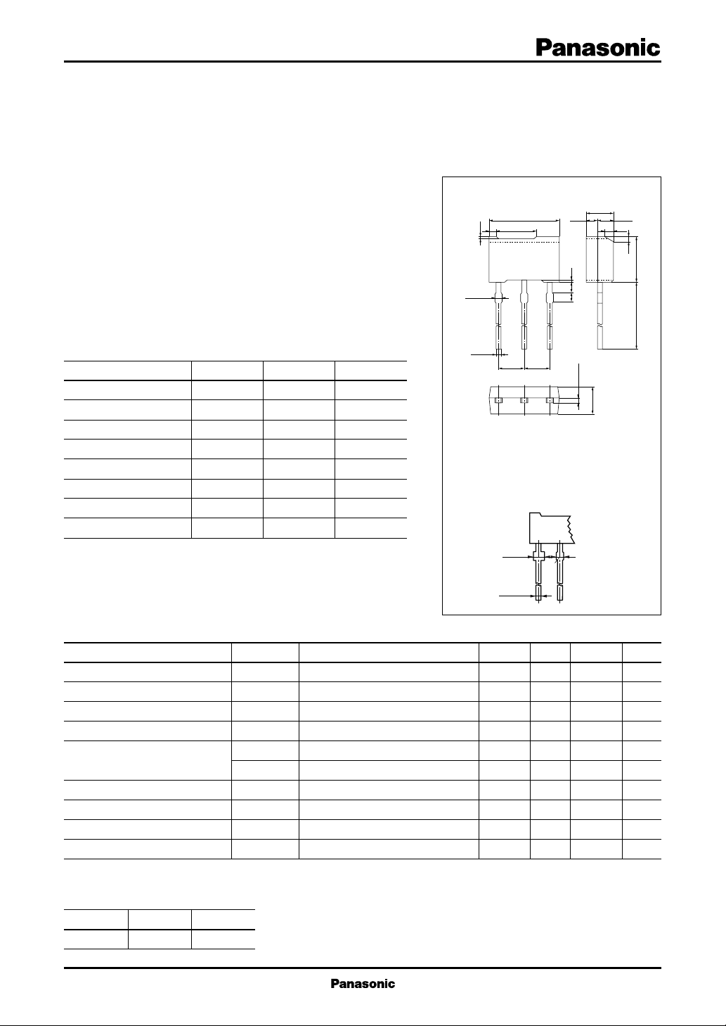
6.9±0.1
4.00.7 0.8
0.15
0.65 max.
+0.1
0.45
–0.05
2.5±0.5 2.5±0.5
Note: In addition to the
lead type shown in
the upper figure, the
type as shown in
the lower figure is
also available.
1.2±0.1
+
0.1
0.45
–
0.05
1.05
±0.05 (1.45)
0.21.01.0
–0.05
+0.1
321
0.45
1:Emitter
2:Collector
3:Base
MT2 Type Package
0.65
max.
Unit: mm
2.5±0.1
0.5
4.5±0.114.5±0.5
2.5±0.1
(HW type)
Electrical Characteristics (Ta=25˚C)
■
Parameter
Collector cutoff current
Collector to base voltage
Collector to emitter voltage
Emitter to base voltage
Forward current transfer ratio
Collector to emitter saturation voltage
Base to emitter saturation voltage
Transition frequency
Collector output capacitance
*1
h
Rank classification
FE1
Symbol
I
CBO
V
CBO
V
CEO
V
EBO
h
FE1
h
FE2
V
CE(sat)
V
BE(sat)
f
T
C
ob
Rank R S
h
FE1
120 ~ 240 170 ~ 340
Conditions
VCB = 20V, IE = 0
IC = 10µA, IE = 0
IC = 1mA, IB = 0
IE = 10µA, IC = 0
*1
*1
VCE = 2V, IC = 200mA
VCE = 2V, IC = 1A
IC = 1A, IB = 50mA
IC = 1A, IB = 50mA
*2
*2
*2
VCB = 10V, IE = –50mA, f = 200MHz
VCB = 10V, IE = 0, f = 1MHz
min
60
60
5
120
80
typ
max
0.15
0.85
110
23
*2
Pulse measurement
0.1
340
0.3
1.2
35
Unit
µA
V
V
V
V
V
MHz
pF
1
Transistor
2SD2177A
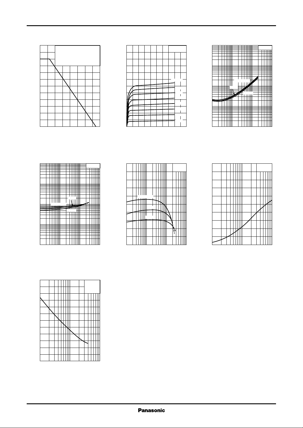
PC — Ta IC — V
1.2
)
W
(
1.0
C
0.8
0.6
0.4
0.2
Collector power dissipation P
0
100
)
V
(
30
BE(sat)
10
3
1
0.3
0.1
0.03
Base to emitter saturation voltage V
0.01
0.01 0.1 1 100.03 0.3 3
Printed circut board: Copper
foil area of 1cm
the board thickness of 1.7mm
for the collector portion.
0 16040 12080 14020 10060
2
or more, and
Ambient temperature Ta (˚C
V
— I
BE(sat)
Ta=–25˚C
C
IC/IB=10
25˚C
100˚C
Collector current IC (A
)
V
CE
)
2.4
2.0
)
A
(
1.6
C
1.2
0.8
Collector current I
0.4
0
0108264
)
Collector to emitter voltage VCE (V
hFE — I
500
FE
400
300
200
100
Ta=100˚C
25˚C
–25˚C
Ta=25˚C
IB=8mA
7mA
6mA
5mA
4mA
3mA
2mA
1mA
)
C
VCE=2V
Forward current transfer ratio h
0
0.01 0.1 1 100.03 0.3 3
Collector current IC (A
)
10
V
(
3
CE(sat)
1
0.3
0.1
0.03
0.01
0.003
0.001
Collector to emitter saturation voltage V
0.01 0.1 1 100.03 0.3 3
Collector current IC (A
200
)
160
MHz
(
T
120
80
40
Transition frequency f
0
–1 –3 –10 –30 –100
Emitter current IE (mA
CE(sat)
Ta=100˚C
25˚C
fT — I
— I
–25˚C
E
C
IC/IB=20
)
VCB=10V
Ta=25˚C
)
)
pF
(
Cob — V
60
50
ob
40
30
20
10
CB
Collector output capacitance C
0
1 3 10 30 100
Collector to base voltage VCB (V
2
IE=0
f=1MHz
Ta=25˚C
)
 Loading...