

Panasonic 2SD2138A, 2SD2138 Datasheet
Po wer Transistors
2SD2138, 2SD2138A
Silicon NPN triple diffusion planar type Darlington
For power amplification
Complementary to 2SB1418 and 2SB1418A
Features
■
●
High forward current transfer ratio hFE which has satisfactory linearity
●
Allowing supply with the radial taping
Absolute Maximum Ratings (T
■
Parameter
Collector to
base voltage
Collector to
emitter voltage
2SD2138
2SD2138A
2SD2138
2SD2138A
Emitter to base voltage
Peak collector current
Collector current
Collector power
dissipation
TC=25°C
Ta=25°C
Junction temperature
Storage temperature
Electrical Characteristics (T
■
Symbol
V
V
V
I
CP
I
C
P
C
T
j
T
stg
Parameter
Collector cutoff
current
Collector cutoff
current
2SD2138
2SD2138A
2SD2138
2SD2138A
Emitter cutoff current
Collector to emitter
voltage
2SD2138
2SD2138A
Forward current transfer ratio
Base to emitter voltage
Collector to emitter saturation voltage
Transition frequency
Turn-on time
Turn-off time
*
h
Rank classification
FE2
Rank Q P
h
FE2
2000 to 5000
4000 to 10000
CBO
CEO
EBO
C
Symbol
I
CBO
I
CEO
I
EBO
V
CEO
h
FE1
*
h
FE2
V
BE
V
CE(sat)
f
T
t
on
t
off
=25˚C)
C
Ratings
60
80
60
80
5
4
2
15
2
150
–55 to +150
=25˚C)
VCE = 60V, IE = 0
VCE = 80V, IE = 0
VCE = 30V, IB = 0
VCE = 40V, IB = 0
VEB = 5V, IC = 0
IC = 30mA, IB = 0
VCE = 4V, IC = 1A
VCE = 4V, IC = 2A
VCE = 4V, IC = 2A
IC = 2A, IB = 8mA
VCE = 10V, IC = 0.5A, f = 1MHz
IC = 2A, IB1 = 8mA, IB2 = –8mA,
VCC = 50V
Unit
V
V
V
A
A
W
˚C
˚C
Conditions
4.2±0.2
13.0±0.2
18.0±0.5
Solder Dip
C1.0
123
2.5±0.2 2.5±0.2
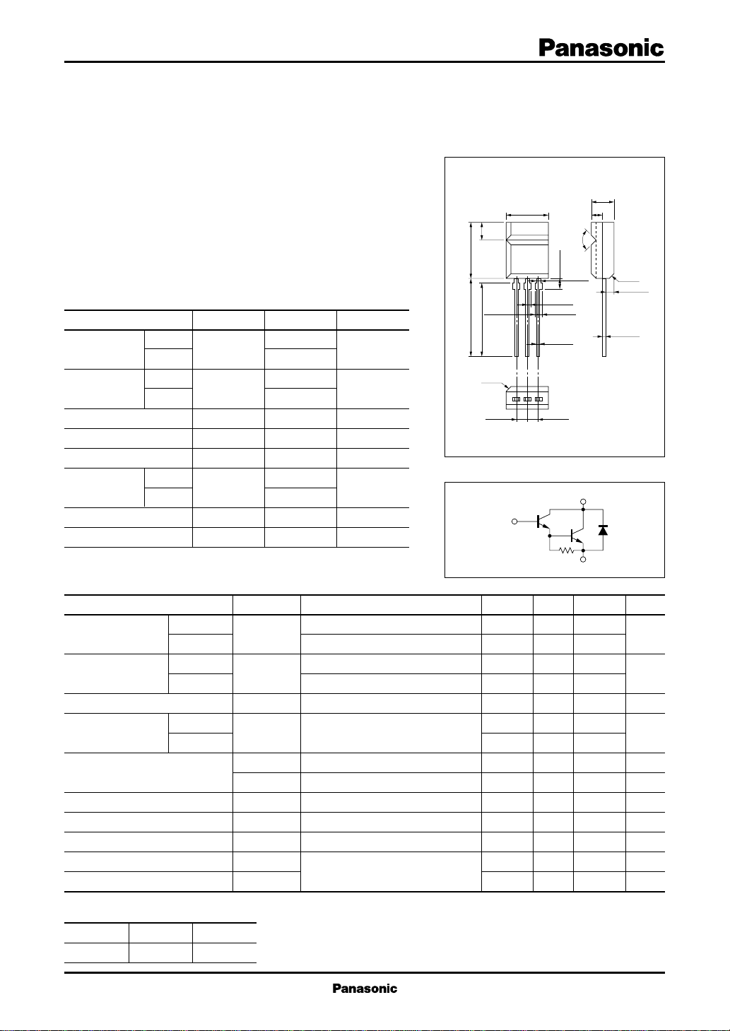
Internal Connection
B
min
60
80
1000
2000
2.5±0.2
0.65±0.1
1.05±0.10.35±0.1
0.55±0.1
typ
20
0.4
4
1.2±0.1
Unit: mm
5.0±0.1
1.010.0±0.2
90°
C1.0
2.25±0.2
0.55±0.1
1:Base
2:Collector
3:Emitter
MT4 Type Package
C
E
max
100
100
100
100
100
Unit
µA
µA
µA
V
10000
2.8
2.5
V
V
MHz
µs
µs
1
Po wer Transistors 2SD2138, 2SD2138A
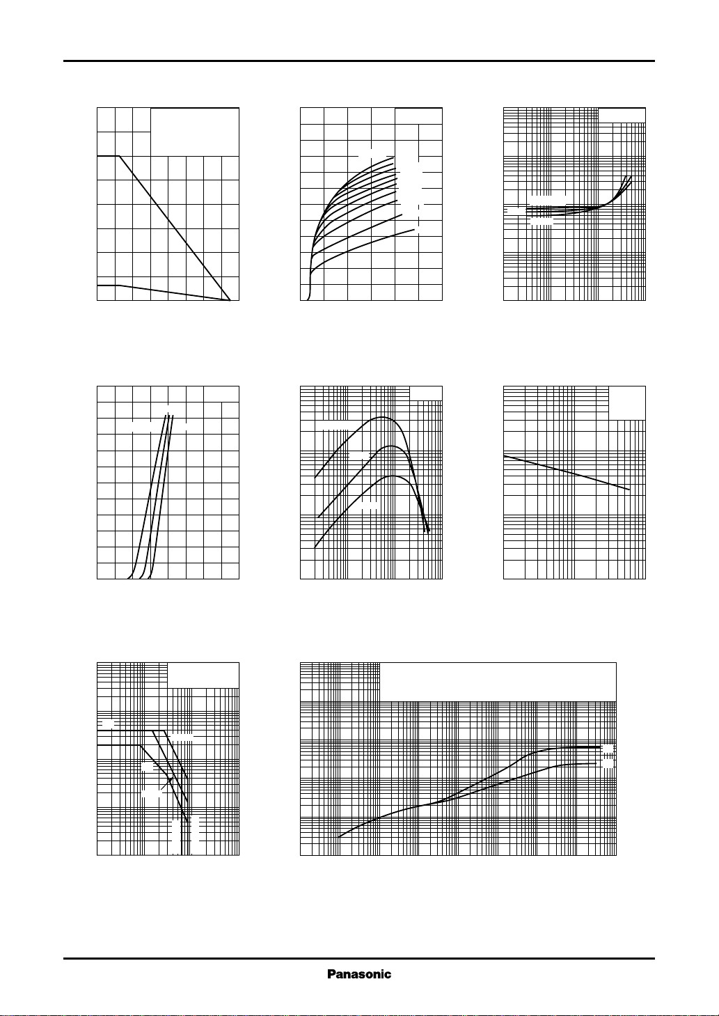
PC—Ta IC—V
20
(1)
(2)
IC—V
TC=100˚C
(1) TC=Ta
(2) Without heat sink
=2.0W)
(P
C
BE
25˚C
–25˚C
)
W
(
C
15
10
5
Collector power dissipation P
0
0 16040 12080 14020 10060
Ambient temperature Ta (˚C
6
5
)
A
(
4
C
3
2
Collector current I
1
0
04132
Base to emitter voltage VBE (V
VCE=4V
CE
6
5
)
A
(
4
C
3
2
IB=2mA
TC=25˚C
1.8mA
1.6mA
1.4mA
1.2mA
1.0mA
0.8mA
0.6mA
0.4mA
0.2mA
Collector current I
1
0
012108264
)
Collector to emitter voltage VCE (V
hFE—I
C
5
10
FE
TC=100˚C
4
10
3
10
25˚C
–25˚C
VCE=4V
)
100
V
(
30
CE(sat)
10
0.3
0.1
0.03
0.01
Collector to emitter saturation voltage V
)
1000
)
pF
(
300
ob
100
30
10
Forward current transfer ratio h
2
10
0.01 0.1 1 100.03 0.3 3
)
Collector current IC (A
)
Collector output capacitance C
V
CE(sat)—IC
IC/IB=250
3
TC=–25˚C
1
25˚C
100˚C
0.01 0.1 1 100.03 0.3 3
CB
)
IE=0
f=1MHz
T
=25˚C
C
Collector current IC (A
Cob—V
3
1
1 3 10 30 100
Collector to base voltage VCB (V
)
Area of safe operation (ASO) R
100
30
)
10
A
(
I
CP
C
3
I
C
1
0.3
0.1
Collector current I
0.03
0.01
1 10 100 10003 30 300
Non repetitive pulse
T
DC
10ms
=25˚C
C
t=1ms
2SD2138
2SD2138A
Collector to emitter voltage VCE (V
10000
)
1000
˚C/W
(
(t)
th
100
10
1
Thermal resistance R
0.1
–4
10
)
–3
10
2
—t
th(t)
Note: Rth was measured at Ta=25˚C and under natural convection.
(1) Without heat sink
(2) With a 50 × 50 × 2mm Al heat sink
–1
–2
10
Time t (s
1010
110
10
)
3
2
(1)
(2)
4
10
 Loading...