

Panasonic 2SD1993 Datasheet
Transistor
2SD1993
Silicon NPN epitaxial planer type
For low-frequency and low-noise amplification
Features
■
●
Low noise voltage NV.
●
High foward current transfer ratio hFE.
●
Allowing supply with the radial taping.
Absolute Maximum Ratings (Ta=25˚C)
■
Parameter
Collector to base voltage
Collector to emitter voltage
Emitter to base voltage
Peak collector current
Collector current
Collector power dissipation
Junction temperature
Storage temperature
Symbol
V
CBO
V
CEO
V
EBO
I
CP
I
C
P
C
T
j
T
stg
Ratings
55
55
7
200
100
400
150
–55 ~ +150
Unit
V
V
V
mA
mA
mW
˚C
˚C
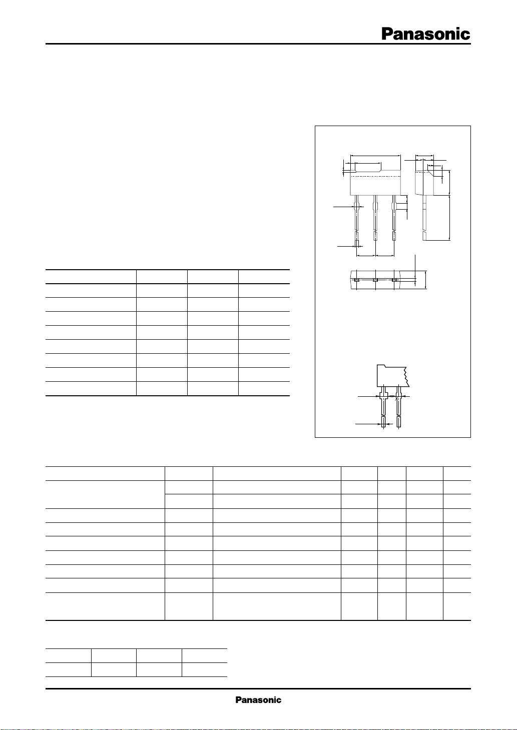
6.9±0.1
0.7 4.0
0.15
0.65 max.
+0.1
0.45
–0.05
2.5±0.5 2.5±0.5
123
Note: In addition to the
lead type shown in
the upper figure, the
type as shown in
the lower figure is
also available.
1.2±0.1
+
0.1
0.45
–
0.05
1.05
±0.05
1.0
0.85
–0.05
+0.1
0.45
1:Emitter
2:Collector
3:Base
MT1 Type Package
0.65
max.
2.5±0.1
2.5±0.1
Unit: mm
(1.45)
0.8
0.8
3.5±0.114.5±0.5
(HW type)
Electrical Characteristics (Ta=25˚C)
■
Parameter
Collector cutoff current
Collector to base voltage
Collector to emitter voltage
Emitter to base voltage
Forward current transfer ratio
Collector to emitter saturation voltage
Transition frequency
Noise voltage
*
hFE Rank classification
Symbol
I
CBO
I
CEO
V
CBO
V
CEO
V
EBO
h
FE
V
CE(sat)
f
T
NV
Rank R S T
h
FE
210 ~ 340 290 ~ 460 360 ~ 650
Conditions
VCB = 20V, IE = 0
VCE = 20V, IB = 0
IC = 10µA, IE = 0
IC = 2mA, IB = 0
IE = 10µA, IC = 0
*
VCE = 10V, IC = 2mA
IC = 100mA, IB = 10mA
VCB = 10V, IE = –2mA, f = 200MHz
VCE = 10V, IC = 1mA, GV = 80dB
Rg = 100kΩ, Function = FLAT
min
55
55
7
210
typ
200
max
100
1
650
1.0
150
Unit
nA
µA
V
V
V
V
MHz
mV
1
Transistor
2SD1993
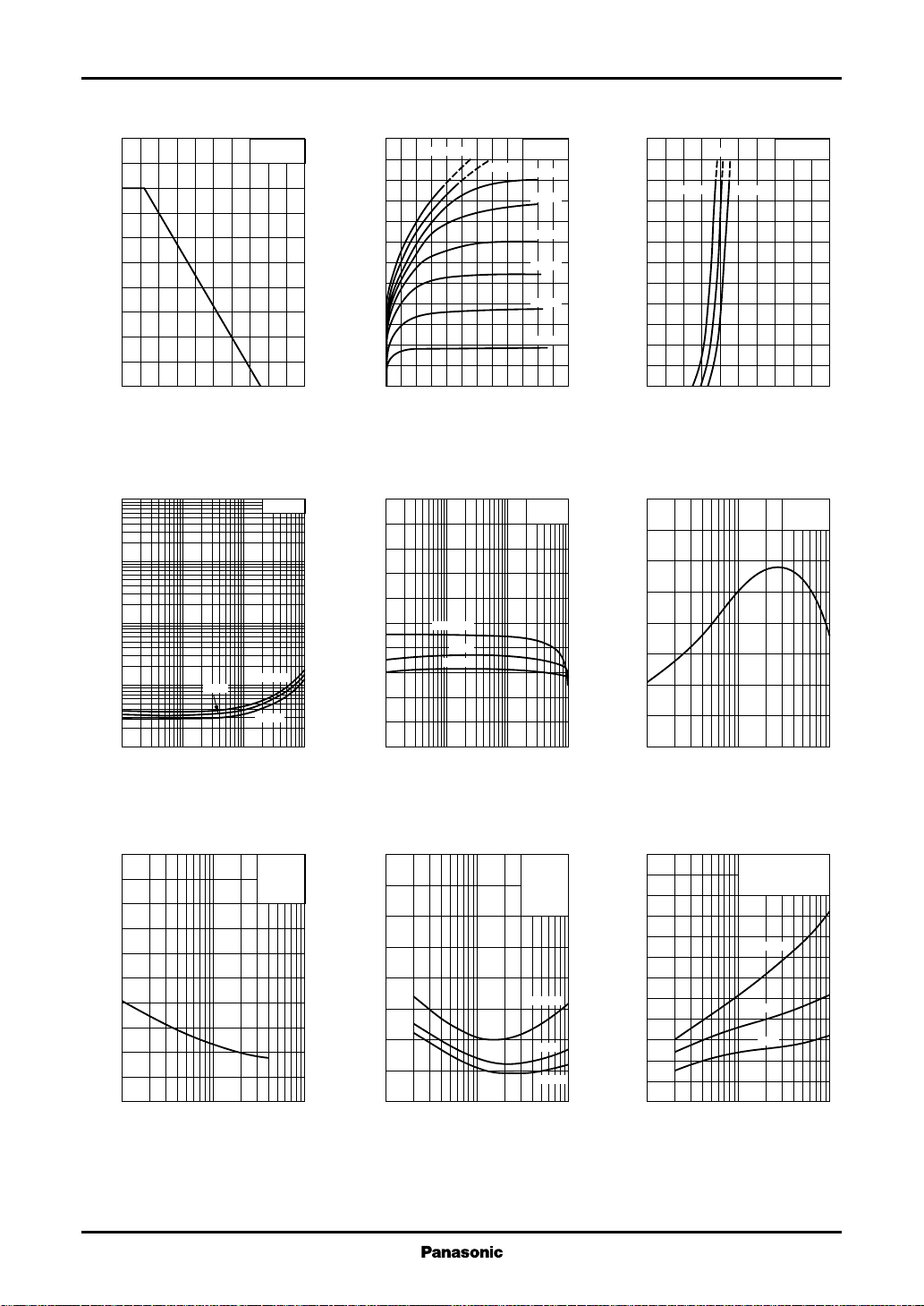
PC — Ta IC — V
500
)
mW
(
400
C
300
200
100
Collector power dissipation P
0
0 20016040 12080
Ambient temperature Ta (˚C
V
CE(sat)
)
100
V
(
30
CE(sat)
10
3
1
0.3
0.1
0.03
0.01
Collector to emitter saturation voltage V
0.1 1 10 1000.3 3 30
Collector current IC (mA
25˚C
— I
Ta=25˚C
)
C
IC/IB=10
Ta=75˚C
–25˚C
)
CE
120
100
)
mA
(
80
C
60
40
Collector current I
20
0
012108264
IB=400µA
350µA
Collector to emitter voltage VCE (V
hFE — I
C
1000
FE
800
600
Ta=75˚C
400
200
25˚C
–25˚C
Forward current transfer ratio h
0
0.1 1 10 1000.3 3 30
Collector current IC (mA
Ta=25˚C
300µA
250µA
200µA
150µA
100µA
50µA
VCE=5V
)
120
100
)
mA
(
80
C
60
40
Collector current I
20
0
02.01.60.4 1.20.8
)
Base to emitter voltage VBE (V
400
350
)
MHz
300
(
T
250
200
150
100
Transition frequency f
50
0
–1 –3 –10 –30 –100
IC — V
BE
–25˚C
VCE=5V
E
VCB=5V
Ta=25˚C
25˚C
Ta=75˚C
fT — I
Emitter current IE (mA
)
)
)
pF
(
Cob — V
10
8
ob
6
4
2
CB
Collector output capacitance C
0
1 3 10 30 100
Collector to base voltage VCB (V
2
IE=0
f=1MHz
Ta=25˚C
)
NF — I
E
8
7
)
6
dB
(
5
4
3
Noise figure NF
2
1
0
–10 –30 –100 –300 –1000
Emitter current IE (µA
VCE=5V
=1kΩ
R
g
Ta=25˚C
f=100Hz
1kHz
10kHz
)
NV — I
C
120
100
)
mV
(
80
60
40
Noise voltage NV
20
0
0.01 0.03 0.1 0.3 1
VCE=10V
G
=80dB
V
Function=FLAT
Rg=100kΩ
22kΩ
5kΩ
Collector current IC (µA
)
 Loading...