

Panasonic 2SD1979 Datasheet
Transistor
V
B
IB=1mA
R
on
= ✕1000(Ω)
f=1kHz
V=0.3V
1kΩ
V
A
V
V
VA–V
B
V
B
2SD1979
Silicon NPN epitaxial planer type
For low-voltage output amplification
For muting
For DC-DC converter
Features
■
●
Low ON resistance Ron.
●
High foward current transfer ratio hFE.
●
S-Mini type package, allowing downsizing of the equipment and
automatic insertion through the tape packing and the magazine
packing.
Absolute Maximum Ratings (Ta=25˚C)
■
Parameter
Collector to base voltage
Collector to emitter voltage
Emitter to base voltage
Peak collector current
Collector current
Collector power dissipation
Junction temperature
Storage temperature
Symbol
V
CBO
V
CEO
V
EBO
I
CP
I
C
P
C
T
j
T
stg
Ratings
50
20
25
500
300
150
150
–55 ~ +150
Unit
V
V
V
mA
mA
mW
˚C
˚C
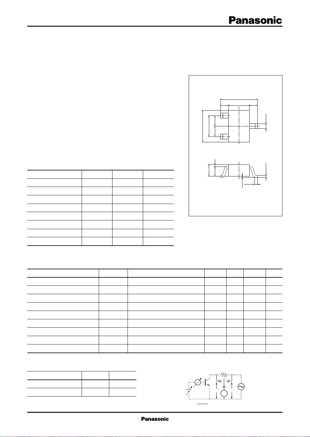
2.1±0.1
1.25±0.1 0.4250.425
1
1.3±0.10.9±0.1
2.0±0.2
0.650.2 0.65
2
0.7±0.1
0.2±0.1
0 to 0.1
1:Base
2:Emitter EIAJ:SC–70
3:Collector S–Mini Type Package
Marking symbol : 3W
3
Unit: mm
–0
+0.1
0.3
–0.05
+0.1
0.15
Electrical Characteristics (Ta=25˚C)
■
Parameter
Collector cutoff current
Emitter cutoff current
Collector to emitter voltage
Forward current transfer ratio
Collector to emitter saturation voltage
Base to emitter voltage
Transition frequency
Collector output capacitance
ON resistanse
*1
hFE Rank classification
Rank S T
h
FE
Marking Symbol 3WS 3WT
Symbol
I
CBO
I
EBO
V
CEO
*1
h
FE
V
CE(sat)
V
BE
f
T
C
ob
*2
R
on
500 ~ 1500 800 ~ 2500
Conditions
VCB = 50V, IE = 0
VEB = 25V, IC = 0
IC = 1mA, IB = 0
VCE = 2V, IC = 4mA
IC = 30mA, IB = 3mA
VCE = 2V, IC = 4mA
VCB = 6V, IE = –4mA, f = 200MHz
VCB = 10V, IE = 0, f = 1MHz
*2
Ron Measurement circuit
min
20
500
typ
0.6
80
4.5
1.0
max
1
1
2500
0.1
Unit
µA
µA
V
V
V
MHz
pF
Ω
1
Transistor
2SD1979
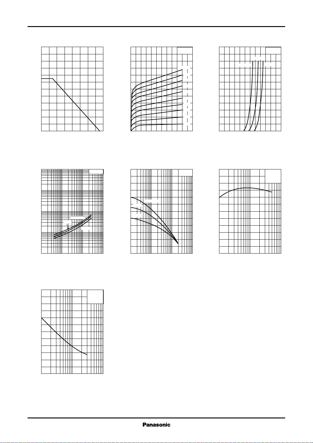
PC — Ta IC — V
240
)
mW
200
(
C
160
120
80
40
Collector power dissipation P
0
0 16040 12080 14020 10060
Ambient temperature Ta (˚C
V
— I
CE(sat)
)
10
V
(
3
CE(sat)
1
0.3
0.1
Ta=75˚C
0.03
0.01
0.003
0.001
Collector to emitter saturation voltage V
0.1 1 10 1000.3 3 30
25˚C
–25˚C
Collector current IC (mA
)
C
IC/IB=10
)
CE
24
20
)
mA
(
16
C
12
8
Collector current I
4
0
012108264
IB=10µA
Collector to emitter voltage VCE (V
hFE — I
C
2400
FE
2000
1600
1200
800
400
Forward current transfer ratio h
Ta=75˚C
25˚C
–25˚C
0
1 10 100 10003 30 300
Collector current IC (mA
Ta=25˚C
9µA
8µA
7µA
6µA
5µA
4µA
3µA
2µA
1µA
VCE=2V
)
120
100
)
mA
80
(
B
60
40
Base current I
20
0
01.21.00.80.2 0.60.4
)
Base to emitter voltage VBE (V
120
)
100
MHz
(
T
80
60
40
20
Transition frequency f
0
–1 –3 –10 –30 –100
IC — V
BE
25˚C
Ta=75˚C
fT — I
–25˚C
E
VCB=6V
Ta=25˚C
Emitter current IE (mA
VCE=2V
)
)
Cob — V
12
)
pF
(
10
ob
8
6
4
2
CB
Collector output capacitance C
0
1 3 10 30 100
Collector to base voltage VCB (V
2
f=1MHz
I
=0
E
Ta=25˚C
)
 Loading...