

Panasonic 2SD1821A, 2SD1821 Datasheet
Transistor
2.1±0.1
1.3±0.10.9±0.1
0.7±0.1
0.3
+0.1
–0
0.15
+0.1
–0.05
2.0±0.2
1.25±0.1 0.4250.425
1
3
2
0.650.2 0.65
0 to 0.1
0.2±0.1
2SD1821, 2SD1821A
Silicon NPN epitaxial planer type
For high breakdown voltage low-frequency and low-noise
amplification
Features
■
●
High collector to emitter voltage V
●
Low noise voltage NV.
●
S-Mini type package, allowing downsizing of the equipment and
automatic insertion through the tape packing and the magazine
packing.
Absolute Maximum Ratings (Ta=25˚C)
■
Parameter
Collector to
base voltage
Collector to
emitter voltage
2SD1821
2SD1821A
2SD1821
2SD1821A
Emitter to base voltage
Peak collector current
Collector current
Collector power dissipation
Junction temperature
Storage temperature
Symbol
V
CBO
V
CEO
V
EBO
I
CP
I
C
P
C
T
j
T
stg
.
CEO
Ratings
–55 ~ +150
150
185
150
185
100
50
150
150
Unit
V
V
5
V
mA
mA
mW
˚C
˚C
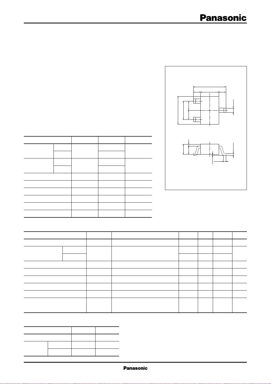
1:Base
2:Emitter EIAJ:SC–70
3:Collector S–Mini Type Package
Marking symbol : P
(2SD1821)
(2SD1821A)
L
Unit: mm
Electrical Characteristics (Ta=25˚C)
■
Parameter
Collector cutoff current
Collector to emitter
voltage
2SD1821
2SD1821A
Emitter to base voltage
Forward current transfer ratio
Collector to emitter saturation voltage
Transition frequency
Collector output capacitance
Noise voltage
*
hFE Rank classification
Marking
Symbol
Rank R S
h
FE
130 ~ 220 185 ~ 330
2SD1821 PR PS
2SD1821A LR LS
Symbol
I
CBO
V
CEO
V
EBO
*
h
FE
V
CE(sat)
f
T
C
ob
NV
Conditions
VCB = 100V, IE = 0
IC = 100µA, IB = 0
IE = 10µA, IC = 0
VCE = 5V, IC = 10mA
IC = 30mA, IB = 3mA
VCB = 10V, IE = –10mA, f = 200MHz
VCB = 10V, IE = 0, f = 1MHz
VCE = 10V, IC = 1mA, GV = 80dB
Rg = 100kΩ, Function = FLAT
min
150
185
5
130
typ
150
2.3
150
max
1
330
1
Unit
µA
V
V
V
MHz
pF
mV
1
Transistor
2SD1821, 2SD1821A
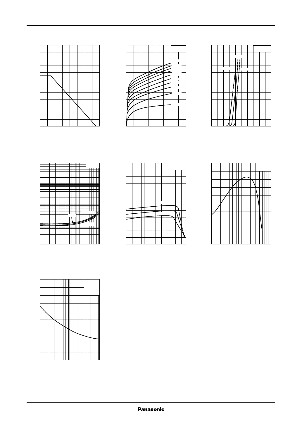
PC — Ta IC — V
240
)
mW
200
(
C
160
120
80
40
Collector power dissipation P
0
0 16040 12080 14020 10060
Ambient temperature Ta (˚C
V
— I
CE(sat)
)
100
V
(
30
CE(sat)
10
3
1
0.3
0.1
0.03
0.01
Collector to emitter saturation voltage V
0.1 1 10 1000.3 3 30
25˚C
Collector current IC (mA
)
C
IC/IB=10
Ta=75˚C
–25˚C
)
CE
120
100
)
mA
(
80
C
60
40
Collector current I
20
0
0164128142106
=2.0mA
I
B
Collector to emitter voltage VCE (V
hFE — I
C
600
FE
500
400
300
200
100
Forward current transfer ratio h
0
0.1 1 10 1000.3 3 30
VCE=10V
Ta=75˚C
25˚C
–25˚C
Collector current IC (mA
Ta=25˚C
1.8mA
1.6mA
1.4mA
1.2mA
1.0mA
0.8mA
0.6mA
0.4mA
0.2mA
)
120
100
)
mA
(
80
C
60
40
Collector current I
20
0
02.01.60.4 1.20.8
)
Base to emitter voltage VBE (V
200
)
160
MHz
(
T
120
80
40
Transition frequency f
0
–1 –3 –10 –30 –100
IC — V
BE
VCE=10V
25˚C
Ta=75˚C
fT — I
–25˚C
E
VCB=10V
Ta=25˚C
Emitter current IE (mA
)
)
)
pF
(
Cob — V
5
4
ob
3
2
1
CB
Collector output capacitance C
0
1 3 10 30 100
Collector to base voltage VCB (V
2
IE=0
f=1MHz
Ta=25˚C
)
 Loading...