

Panasonic 2SD1820A User Manual
This product complies with the RoHS Directive (EU 2002/95/EC).
Transistors
2SD1820A
Silicon NPN epitaxial planar type
For general amplification
Complementary to 2SB1219A
Features
Low collector-emitter saturation voltage V
S-Mini type package, allowing downsizing of the equipment and automatic
insertion through the tape packing.
CE(sat)
Package
Code
SMini3-G1
Pin Name
1. Base
Absolute Maximum Ratings Ta = 25°C
Parameter Symbol Rating Unit
Collector-base voltage (Emitter open) V
Collector-emitter voltage (Base open) V
Emitter-base voltage (Collector open) V
Collector current I
Peak collector current I
Collector power dissipation P
Junction temperature T
Storage temperature T
CBO
CEO
EBO
C
CP
C
j
stg
60 V
50 V
5 V
500 mA
1 A
150 mW
150
–55 to +150
°C
°C
2. Emitter
3. Collector
Marking Symbol: X
Electrical Characteristics Ta = 25°C±3°C
Parameter Symbol Conditions Min Typ Max Unit
Collector-base voltage (Emitter open) V
Collector-emitter voltage (Base open) V
Emitter-base voltage (Collector open) V
Collector-base cutoff current (Emitter open)
1
Forward current transfer ratio
Collector-emitter saturation voltage
*
1
*
Transition frequency f
Collector output capacitance
(Common base, input open circuited)
Note) 1. Measuring methods are based on JAPANESE INDUSTRIAL STANDARD JIS C 7030 measuring methods for transistors.
2. *1: Pulse measurement
*2: Rank classification
Product of no-rank is not classified and have no marking symbol for rank.
Rank Q R S No-rank
h
FE1
Marking symbol XQ XR XS X
85 to 170 120 to 240 170 to 340 85 to 340
CBOIC
CEOIC
EBOIE
I
CBO
h
FE1
h
FE2
V
CE(sat)IC
T
C
ob
= 10 mA, IE = 0 60 V
= 2 mA, IB = 0 50 V
= 10 mA, IC = 0 5 V
VCB = 20 V, IE = 0 0.1
2
*
VCE = 10 V, IC = 150 mA 85 340
VCE = 10 V, IC = 500 mA 40
= 300 mA, IB = 30 mA 0.35 0.60 V
VCB = 10 V, IE = –50 mA, f = 200 MHz 200 MHz
VCB = 10 V, IE = 0, f = 1 MHz 6 15 pF
mA
Publication date : October 2008 SJC00424AED 1
This product complies with the RoHS Directive (EU 2002/95/EC).
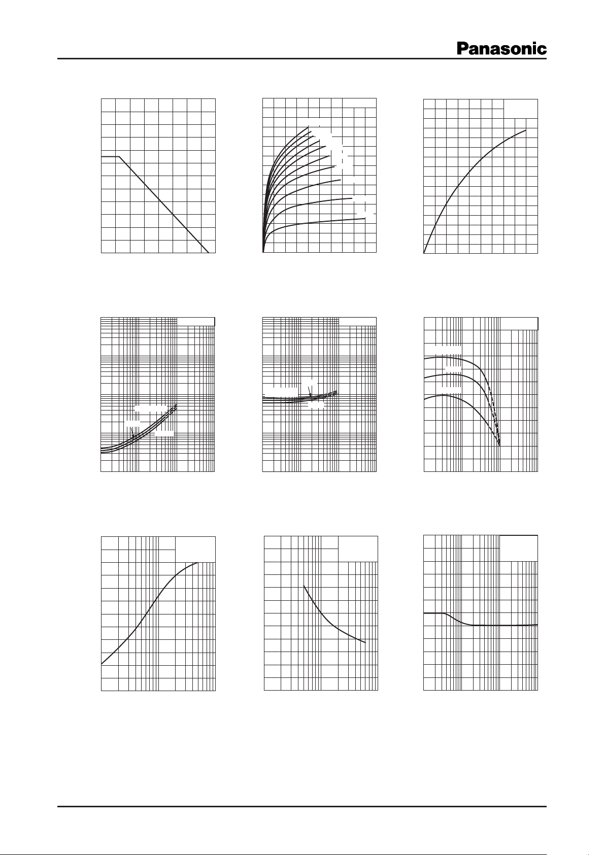
0 16040 12080
0
240
200
160
120
80
40
Collector power dissipation P
C
(
mW
)
Ambient temperature Ta (°C
)
0 20164 128
0
800
600
200
500
700
400
100
300
Ta = 25°C
IB = 10 mA
9 mA
8 mA
7 mA
6 mA
5 mA
4 mA
3 mA
2 mA
1 mA
Collector current I
C
(
mA
)
Collector-emitter voltage VCE (V
)
0.01 0.1 1 10
0.01
0.1
1
10
100
IC / IB = 10
25°C
−25°C
Ta = 75°C
Collector-emitter saturation voltage V
CE(sat)
(
V
)
Collector current IC (A
)
0.01 0.1 1 10
0.01
0.1
1
10
100
IC / IB = 10
Ta = −25°C
25°C
75°C
Base-emitter saturation voltage V
BE(sat)
(
V
)
Collector current IC (A
)
0.01 0.1 1 10
0
300
250
200
150
100
50
VCE = 10 V
Ta = 75°C
25°C
−25°C
Forward current transfer ratio h
FE
Collector current IC (A
)
−1 −10 −100
0
240
200
160
120
80
40
VCB = 10 V
Ta = 25°C
Transition frequency f
T
(
MHz
)
Emitter current IE (mA
)
1 10 100
0
12
10
8
6
4
2
IE = 0
f = 1 MHz
Ta = 25°C
Collector-base voltage VCB (V
)
Collector output capacitance
(Common base, input open circuited)
C
ob
(pF)
1 10 100 1000
0
120
100
80
60
40
20
IC = 2 mA
Ta = 25°C
Base-emitter resistance RBE (kΩ
)
Collector-emitter voltage
(Resistor between B and E)
V
CER
(V)
0 1082 64
0
800
600
200
500
700
400
100
300
VCE = 10 V
Ta = 25°C
Base current IB (mA
)
Collector current I
C
(
mA
)
2SD1820A
PC Ta IC VCE IC I
V
IC V
CE(sat)
BE(sat)
I
C
hFE I
B
C
fT IE Cob V
2 SJC00424AED
V
CB
CER
R
BE
 Loading...