

Panasonic 2SD1820 Datasheet
Transistor
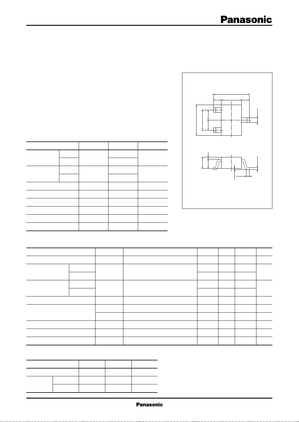
2.1±0.1
1.3±0.10.9±0.1
0.7±0.1
0.3
+0.1
–0
0.15
+0.1
–0.05
2.0±0.2
1.25±0.1 0.4250.425
1
3
2
0.650.2 0.65
0 to 0.1
0.2±0.1
2SD1820, 2SD1820A
Silicon NPN epitaxial planer type
For general amplification
Complementary to 2SB1219 and 2SB1219A
Features
■
●
Low collector to emitter saturation voltage V
●
S-Mini type package, allowing downsizing of the equipment and
automatic insertion through the tape packing and the magazine
packing.
Absolute Maximum Ratings (Ta=25˚C)
■
Parameter
Collector to
base voltage
Collector to
emitter voltage
2SD1820
2SD1820A
2SD1820
2SD1820A
Emitter to base voltage
Peak collector current
Collector current
Collector power dissipation
Junction temperature
Storage temperature
Symbol
V
CBO
V
CEO
V
EBO
I
CP
I
C
P
C
T
j
T
stg
Ratings
30
60
25
50
500
150
150
–55 ~ +150
5
1
CE(sat)
.
Unit
V
V
V
A
mA
mW
˚C
˚C
1:Base
2:Emitter EIAJ:SC–70
3:Collector S–Mini Type Package
Marking symbol : W
(2SD1820)
(2SD1820A)
X
Unit: mm
Electrical Characteristics (Ta=25˚C)
■
Parameter
Collector cutoff current
Collector to base
voltage
Collector to emitter
voltage
2SD1820
2SD1820A
2SD1820
2SD1820A
Emitter to base voltage
Forward current transfer ratio
Collector to emitter saturation voltage
Transition frequency
Collector output capacitance
*1
h
Rank classification
FE1
Marking
Symbol
Rank Q R S
h
FE1
85 ~ 170 120 ~ 240 170 ~ 340
2SD1820 WQ WR WS
2SD1820A XQ XR XS
Symbol
I
CBO
V
CBO
V
CEO
V
EBO
*1
h
FE1
h
FE2
V
CE(sat)
f
T
C
ob
Conditions
VCB = 20V, IE = 0
IC = 10µA, IE = 0
IC = 2mA, IB = 0
IE = 10µA, IC = 0
VCE = 10V, IC = 150mA
VCE = 10V, IC = 500mA
IC = 300mA, IB = 30mA
*2
*2
*2
VCB = 10V, IE = –50mA*2, f = 200MHz
VCB = 10V, IE = 0, f = 1MHz
min
30
60
25
50
5
85
40
typ
160
max
340
0.35
200
6
*2
Pulse measurement
0.1
0.6
15
Unit
µA
V
V
V
V
MHz
pF
1
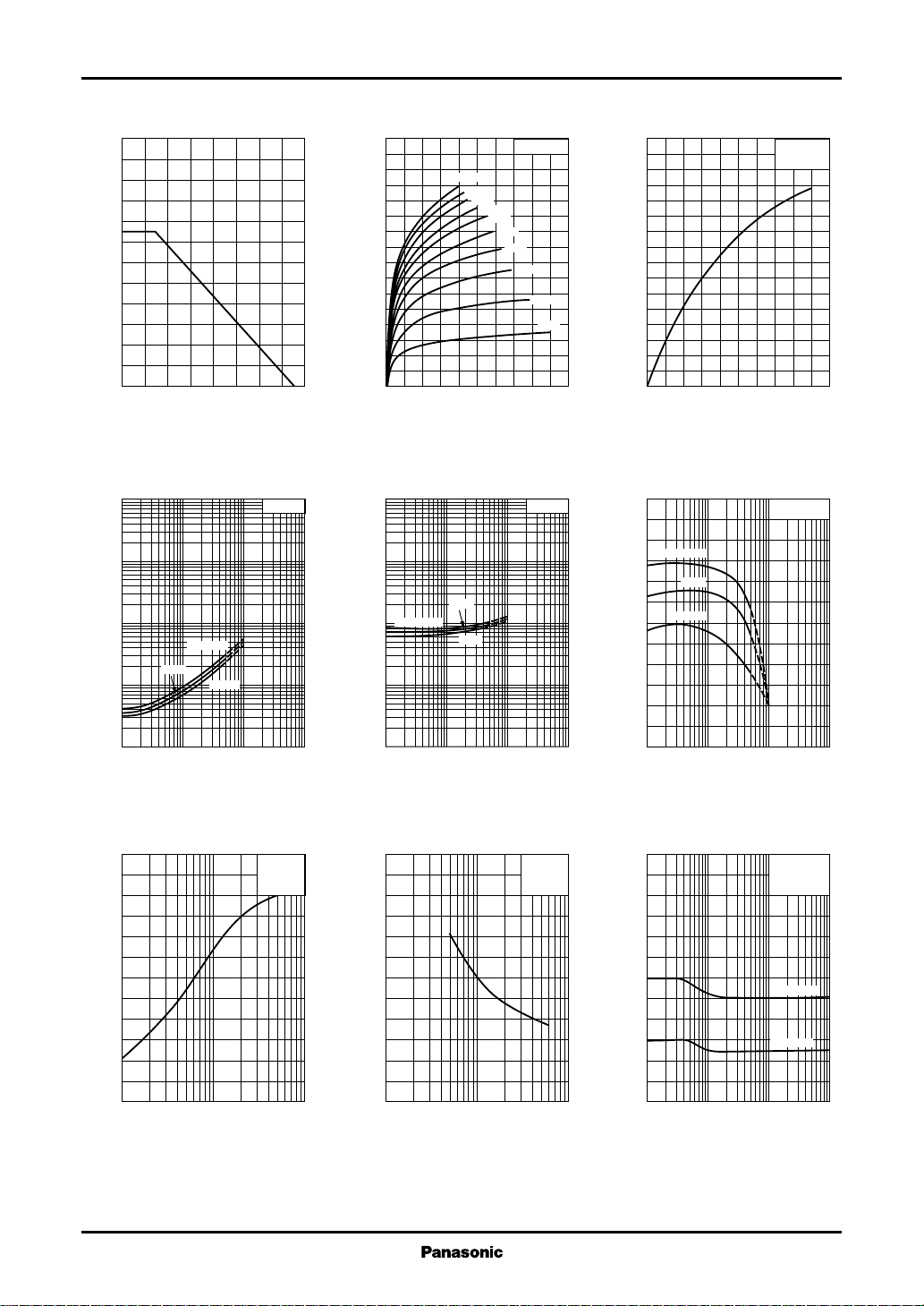
Transistor
2SD1820, 2SD1820A
PC — Ta IC — V
240
)
mW
200
(
C
160
120
80
40
Collector power dissipation P
0
0 16040 12080 14020 10060
Ambient temperature Ta (˚C
V
— I
CE(sat)
)
100
V
(
30
CE(sat)
10
3
1
0.3
0.1
0.03
0.01
Collector to emitter saturation voltage V
0.01 0.1 1 100.03 0.3 3
Ta=75˚C
25˚C
–25˚C
Collector current IC (A
)
C
IC/IB=10
)
CE
800
700
)
600
mA
(
C
500
400
300
200
Collector current I
100
0
020164128
IB=10mA
9mA
8mA
7mA
6mA
Ta=25˚C
5mA
4mA
3mA
2mA
1mA
Collector to emitter voltage VCE (V
V
— I
BE(sat)
100
)
V
(
30
BE(sat)
10
3
Ta=–25˚C
1
0.3
0.1
0.03
Base to emitter saturation voltage V
0.01
0.01 0.1 1 100.03 0.3 3
25˚C
Collector current IC (A
C
IC/IB=10
75˚C
)
800
700
)
600
mA
(
C
500
400
300
200
Collector current I
100
0
0108264
)
Base current IB (mA
hFE — I
300
FE
250
Ta=75˚C
200
150
100
Forward current transfer ratio h
25˚C
–25˚C
50
0
0.01 0.1 1 100.03 0.3 3
Collector current IC (A
IC — I
B
VCE=10V
Ta=25˚C
)
C
VCE=10V
)
fT — I
E
240
)
200
MHz
(
T
160
120
80
40
Transition frequency f
0
–1 –3 –10 –30 –100
Emitter current IE (mA
2
VCB=10V
Ta=25˚C
)
)
pF
(
Cob — V
12
10
ob
8
6
4
2
CB
Collector output capacitance C
0
1 3 10 30 100
Collector to base voltage VCB (V
IE=0
f=1MHz
Ta=25˚C
120
)
V
(
100
CER
80
60
40
20
Collector to emitter voltage V
0
1 10 100 10003 30 300
)
Base to emitter resistance RBE (kΩ
V
— R
CER
BE
2SD1820A
2SD1820
IC=2mA
Ta=25˚C
)
 Loading...