

Panasonic 2SD1772A, 2SD1772 Datasheet
Po wer Transistors
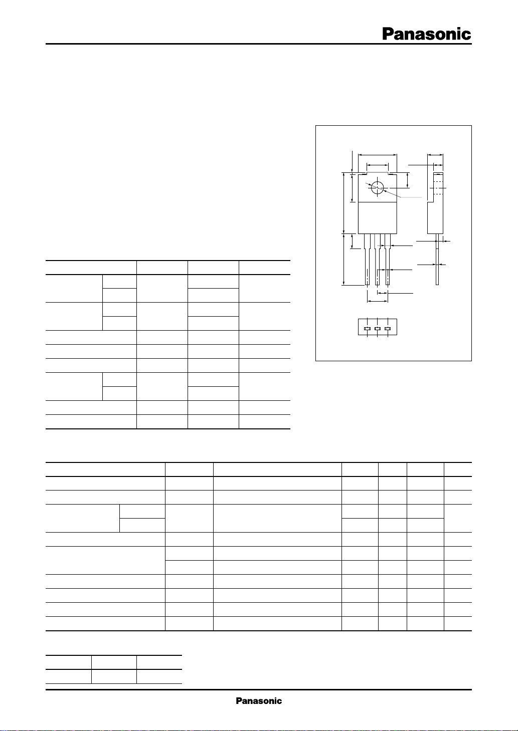
10.0±0.2
5.5±0.2
7.5±0.2
16.7±0.3
0.7±0.1
14.0±0.5
Solder Dip
4.0
0.5
+0.2
–0.1
1.4±0.1
1.3±0.2
0.8±0.1
2.54±0.25
5.08±0.5
213
2.7±0.2
4.2±0.2
4.2±0.2
φ3.1±0.1
2SD1772, 2SD1772A
Silicon NPN triple diffusion planar type
For power amplification
For TV vertical deflection output
Complementary to 2SB1192 and 2SB1192A
Features
■
●
Large collector power dissipation P
●
Full-pack package which can be installed to the heat sink with
one screw
Absolute Maximum Ratings (T
■
Parameter
Collector to
base voltage
Collector to
emitter voltage
2SD1772
2SD1772A
2SD1772
2SD1772A
Emitter to base voltage
Peak collector current
Collector current
Collector power
dissipation
TC=25°C
Ta=25°C
Junction temperature
Storage temperature
Symbol
V
V
V
I
CP
I
C
P
T
T
CBO
CEO
EBO
C
j
stg
C
=25˚C)
C
Ratings
200
200
150
180
6
2
1
25
2
150
–55 to +150
Unit
V
V
V
A
A
W
˚C
˚C
Unit: mm
1:Base
2:Collector
3:Emitter
TO–220 Full Pack Package(a)
Electrical Characteristics (T
■
Parameter
Collector cutoff current
Emitter cutoff current
Collector to emitter
voltage
Emitter to base voltage
Forward current transfer ratio
Base to emitter voltage
Collector to emitter saturation voltage
Transition frequency
Collector output capacitance
*
h
Rank classification
FE1
Rank Q P
h
FE1
60 to 140 100 to 240
2SD1772
2SD1772A
C
Symbol
I
CBO
I
EBO
V
CEO
V
EBO
*
h
FE1
h
FE2
V
BE
V
CE(sat)
f
T
C
ob
=25˚C)
Conditions
VCB = 200V, IE = 0
VEB = 4V, IC = 0
IC = 5mA, IB = 0
IE = 0.5mA, IC = 0
VCE = 10V, IC = 100mA
VCE = 10V, IC = 300mA
VCE = 10V, IC = 300mA
IC = 500mA, IB = 50mA
VCE = 10V, IC = 100mA, f = 1MHz
VCB = 10V, IE = 0, f = 1MHz
min
150
180
6
60
50
typ
20
27
max
50
50
240
1
1
Unit
µA
µA
V
V
V
V
MHz
pF
1
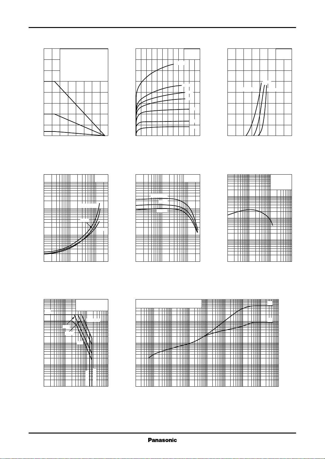
Po wer Transistors 2SD1772, 2SD1772A
PC—Ta IC—V
40
)
35
W
(
C
30
25
20
15
10
5
Collector power dissipation P
0
0 16040 12080 14020 10060
)
V
(
10
CE(sat)
3
1
0.3
0.1
0.03
0.01
Collector to emitter saturation voltage V
0.01 310.10.03 0.3
(1) TC=Ta
(2) With a 100 × 100 × 2mm
Al heat sink
(3) Without heat sink
=2W)
(P
(1)
(2)
(3)
C
Ambient temperature Ta (˚C
V
CE(sat)—IC
IC/IB=10
TC=100˚C
25˚C
–25˚C
Collector current IC (A
)
)
CE
1.6
1.4
)
1.2
A
(
C
1.0
0.8
0.6
0.4
Collector current I
0.2
0
02420164128
IB=20mA
10mA
Collector to emitter voltage VCE (V
hFE—I
C
1000
FE
300
100
30
10
Forward current transfer ratio h
TC=100˚C
25˚C
–25˚C
3
1
0.01 310.10.03 0.3
VCE=10V
Collector current IC (A
T
8mA
6mA
=25˚C
C
4mA
2mA
1mA
)
4
)
3
A
(
C
2
1
Collector current I
0
01.60.4 1.20.8
)
Base to emitter voltage VBE (V
1000
300
)
MHz
100
(
T
30
10
3
1
Transition frequency f
0.3
0.1
0.01 0.1 1 100.03 0.3 3
IC—V
BE
V
25˚C
TC=100˚C
fT —I
–25˚C
C
VCE=10V
f=1MHz
T
C
Collector current IC (A
CE
=25˚C
=10V
)
)
Area of safe operation (ASO) R
10
3
I
CP
I
)
C
1
A
(
C
0.3
0.1
0.03
0.01
Collector current I
0.003
0.001
1 10 100 10003 30 300
1ms
10ms
Non repetitive pulse
=25˚C
T
C
t=0.5ms
DC
2SD1772
Collector to emitter voltage VCE (V
2SD1772A
)
2
10
(1) Without heat sink
(2) With a 100 × 100 × 2mm Al heat sink
)
˚C/W
(
10
(t)
th
1
–1
10
Thermal resistance R
–2
10
–4
10
–3
10
2
—t
th(t)
(1)
(2)
–1
–2
10
Time t (s
1010
110
10
)
3
2
4
10
 Loading...