

Panasonic 2SC4782 Datasheet
Transistor
2.8
+0.2
–0.3
1.5
+0.25
–0.050.65±0.15 0.65±0.15
3
1
2
0.950.95
1.9±0.2
0.4
+0.1
–0.05
1.1
+0.2
–0.1
0.8
0.4±0.2
0 to 0.1
0.16
+0.1
–0.06
1.45
0.1 to 0.3
2.9
+0.2
–0.05
2SC4782
Silicon NPN epitaxial planer type
For high speed switching
Features
■
●
High-speed switching.
●
Low collector to emitter saturation voltage V
●
Mini type package, allowing downsizing of the equipment and
automatic insertion through the tape packing and the magazine
packing.
Absolute Maximum Ratings (Ta=25˚C)
■
Parameter
Collector to base voltage
Collector to emitter voltage
Emitter to base voltage
Peak collector current
Collector current
Collector power dissipation
Junction temperature
Storage temperature
Symbol
V
CBO
V
CES
V
EBO
I
CP
I
C
P
C
T
j
T
stg
Ratings
25
20
300
200
200
150
–55 ~ +150
5
CE(sat)
.
Unit
V
V
V
mA
mA
mW
˚C
˚C
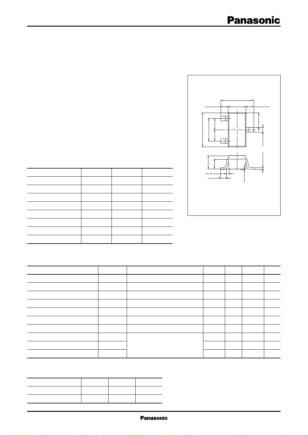
Unit: mm
1:Base JEDEC:TO–236
2:Emitter EIAJ:SC–59
3:Collector Mini T ype Package
Marking symbol : DV
Electrical Characteristics (Ta=25˚C)
■
Parameter
Collector cutoff current
Emitter cutoff current
Forward current transfer ratio
Collector to emitter saturation voltage
Base to emitter saturation voltage
Transition frequency
Collector output capacitance
Turn-on time
Turn-off time
Storage time
*
hFE Rank classification
Marking Symbol DVP DVQ DVR
Rank P Q R
h
FE
Symbol
I
I
h
V
V
f
C
t
t
t
CBO
EBO
FE
T
on
off
stg
*
CE(sat)
BE(sat)
ob
VCB = 10V, IE = 0
VEB = 4V, IC = 0
VCE = 1V, IC = 10mA
IC = 10mA, IB = 1mA
IC = 10mA, IB = 1mA
VCB = 10V, IE = –10mA, f = 200MHz
VCB = 10V, IE = 0, f = 1MHz
Refer to the measurment circuit
40 ~ 80 60 ~ 120 90 ~ 200
Conditions
min
40
200
typ
0.17
0.76
500
2
17
15
7
max
0.1
0.1
200
0.25
1.0
4
Unit
µA
µA
V
V
MHz
pF
ns
ns
ns
1
Transistor
2SC4782
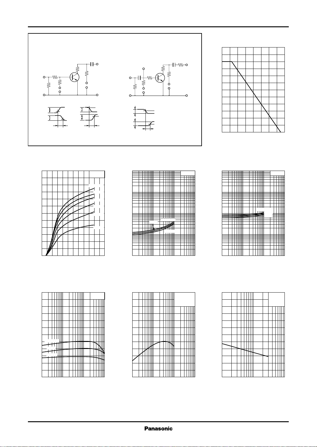
Switching time measurement circuit
t
, t
Test Circuit t
on
off
0.1µF
3.3kΩ
t
10%
on
3.3kΩ
V
bb
–3V
90%
220Ω
=
=10V
V
in
50Ω
V
in
V
out
IC — V
120
100
)
mA
(
80
C
60
40
Collector current I
20
0
01.21.00.80.2 0.60.4
Collector to emitter voltage VCE (V
50Ω
=3V
V
CC
V
in
V
out
t
off
CE
Ta=25˚C
IB=3.0mA
2.5mA
2.0mA
1.5mA
1.0mA
0.5mA
10%
V
90%
PC — Ta
T est Circuit
stg
out
Vin=10V
0.1µF
50Ω
0
V
in
V
out
(Waveform at A)
A
500Ω
500Ω
=2V
V
bb
t
stg
V
)
100
V
(
30
CE(sat)
10
3
1
0.3
0.1
0.03
0.01
Collector to emitter saturation voltage V
1 10 100 10003 30 300
)
25˚C
Collector current IC (mA
910Ω
10%
10%
CE(sat)
0.1µF
— I
Ta=75˚C
–25˚C
1kΩ
90Ω
VCC=10V
C
V
IC/IB=10
)
out
240
)
mW
200
(
C
160
120
80
40
Collector power dissipation P
0
0 16040 12080 14020 10060
Ambient temperature Ta (˚C
V
— I
BE(sat)
100
)
V
(
30
BE(sat)
10
3
1
0.3
0.1
0.03
Base to emitter saturation voltage V
0.01
1 10 100 10003 30 300
C
Ta=–25˚C
25˚C
75˚C
IC/IB=10
Collector current IC (mA
)
)
hFE — I
C
240
FE
200
160
120
Ta=75˚C
25˚C
80
–25˚C
40
Forward current transfer ratio h
0
0.1 1 10 1000.3 3 30
Collector current IC (mA
2
VCE=1V
)
fT — I
1200
)
1000
MHz
(
T
800
600
400
200
Transition frequency f
0
–1 –10 –100 –1000–3 –30 –300
Emitter current IE (mA
E
VCB=10V
Ta=25˚C
f=200MHz
)
)
pF
(
Cob — V
6
5
ob
4
3
2
1
CB
Collector output capacitance C
0
1 3 10 30 100
Collector to base voltage VCB (V
IE=0
f=1MHz
Ta=25˚C
)
 Loading...